
© 2008 Microchip Technology Inc.
DS21811E-page 1
MCP6281/1R/2/3/4/5
Features
• Gain Bandwidth Product: 5 MHz (typical)
• Supply Current: I
Q
= 450 µA (typical)
• Supply Voltage: 2.2V to 6.0V
• Rail-to-Rail Input/Output
• Extended Temperature Range: -40°C to +125°C
• Available in Single, Dual, and Quad Packages
• Single with CS (MCP6283)
• Dual with CS (MCP6285)
Applications
• Automotive
• Portable Equipment
• Photodiode Amplifier
• Analog Filters
• Notebooks and PDAs
• Battery-Powered Systems
Design Aids
• SPICE Macro Models
• FilterLab
®
Software
• Mindi™ Circuit Designer & Simulator
• MAPS (Microchip Advanced Part Selector)
• Analog Demonstration and Evaluation Boards
• Application Notes
Description
The Microchip Technology Inc. MCP6281/1R/2/3/4/5
family of operational amplifiers (op amps) provide wide
bandwidth for the current. This family has a 5 MHz Gain
Bandwidth Product (GBWP) and a 65° phase margin.
This family also operates from a single supply voltage
as low as 2.2V, while drawing 450 µA (typical) quiescent
current. Additionally, the MCP6281/1R/2/3/4/5 supports
rail-to-rail input and output swing, with a common mode
input voltage range of V
DD
+ 300 mV to V
SS
– 300 mV.
This family of operational amplifiers is designed with
Microchip’s advanced CMOS process.
The MCP6285 has a Chip Select (CS) input for dual op
amps in an 8-pin package. This device is manufactured
by cascading the two op amps (the output of op amp A
connected to the non-inverting input of op amp B). The
CS input puts the device in Low-power mode.
The MCP6281/1R/2/3/4/5 family operates over the
Extended Temperature Range of -40°C to +125°C. It
also has a power supply range of 2.2V to 6.0V.
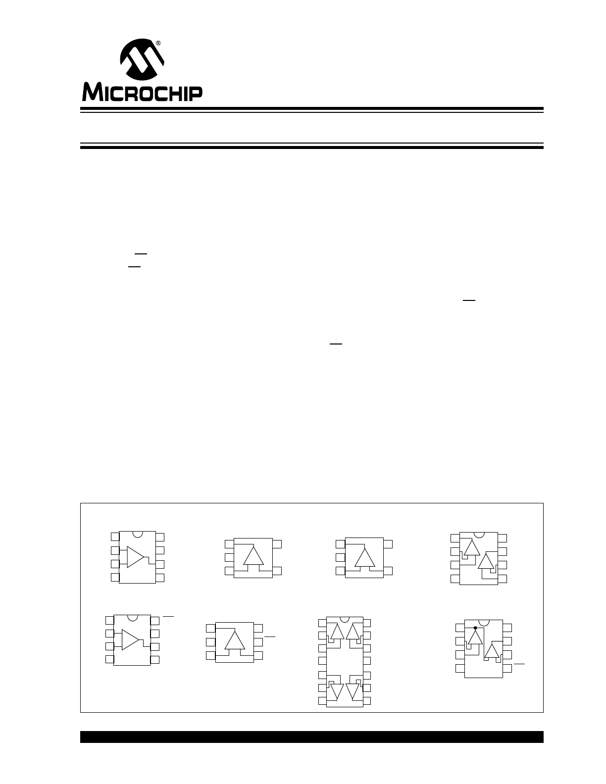
Package Types
V
IN
_
MCP6281
V
DD
1
2
3
4
8
7
6
5
-
+
NC
NC
NC
V
IN
+
V
SS
MCP6282
PDIP, SOIC, MSOP
MCP6284
1
2
3
4
14
13
12
11
-
+ -
+
10
9
8
5
6
7
+
-
-
+
PDIP, SOIC, TSSOP
1
2
3
4
8
7
6
5
-
+ -
+
V
OUT
MCP6283
1
2
3
4
8
7
6
5
-
+
V
INA
_
V
INA
+
V
SS
V
OUTA
V
OUTB
V
DD
V
INB
_
V
INB
+
V
SS
V
IN
+
V
IN
_
NC
CS
V
DD
V
OUT
NC
V
OUTA
V
INA
_
V
INA
+
V
DD
V
SS
V
OUTB
V
INB
_
V
INB
+
V
OUTC
V
INC
_
V
INC
+
V
OUTD
V
IND
_
V
IND
+
PDIP, SOIC, MSOP
PDIP, SOIC, MSOP
MCP6285
PDIP, SOIC, MSOP
1
2
3
4
8
7
6
5
+ -
V
INA
_
V
INA
+
V
SS
V
OUTA
/V
INB
+
V
OUTB
V
DD
V
INB
_
CS
- +
MCP6281
SOT-23-5
4
1
2
3
-
+
5 V
DD
V
IN
–
V
OUT
V
SS
V
IN
+
MCP6281R
SOT-23-5
4
1
2
3
-
+
5 V
SS
V
IN
–
V
OUT
V
DD
V
IN
+
MCP6283
SOT-23-6
4
1
2
3
-
+
6
5
V
SS
V
IN
+
V
OUT
CS
V
DD
V
IN
_
450 µA, 5 MHz Rail-to-Rail Op Amp
MCP6281/1R/2/3/4/5
DS21811E-page 2
© 2008 Microchip Technology Inc.
1.0
ELECTRICAL
CHARACTERISTICS
Absolute Maximum Ratings †
V
DD
– V
SS
........................................................................7.0V
Current at Input Pins ....................................................±2 mA
Analog Inputs (V
IN
+, V
IN
–) †† ........ V
SS
– 1.0V to V
DD
+ 1.0V
All Other Inputs and Outputs ......... V
SS
– 0.3V to V
DD
+ 0.3V
Difference Input Voltage ...................................... |V
DD
– V
SS
|
Output Short Circuit Current .................................Continuous
Current at Output and Supply Pins ............................±30 mA
Storage Temperature.................................... –65°C to +150°C
Maximum Junction Temperature (T
J
) ......................... .+150°C
ESD Protection On All Pins (HBM; MM)
.............. ≥ 4 kV; 400V
† Notice: Stresses above those listed under “Absolute
Maximum Ratings” may cause permanent damage to the
device. This is a stress rating only and functional operation of
the device at those or any other conditions above those
indicated in the operational listings of this specification is not
implied. Exposure to maximum rating conditions for extended
periods may affect device reliability.
†† See Section 4.1.2 “Input Voltage and Current Limits”.
DC ELECTRICAL SPECIFICATIONS
Electrical Characteristics: Unless otherwise indicated, T
A
= +25 C, V
DD
= +2.2V to +5.5V, V
SS
= GND, V
OUT
≈ V
DD
/2,
V
CM
= V
DD
/2, V
L
= V
DD
/2, R
L
= 10 k
Ω to V
L
and CS is tied low. (refer to
Figure 1-2
and
Figure 1-3
).
Parameters
Sym
Min
Typ
Max
Units
Conditions
Input Offset
Input Offset Voltage
V
OS
-3.0
—
+3.0
mV
V
CM
= V
SS
(Note 1)
Input Offset Voltage
(Extended Temperature)
V
OS
-5.0
—
+5.0
mV
T
A
= -40°C to +125°C,
V
CM
= V
SS
(Note 1)
Input Offset Temperature Drift
ΔV
OS
/
ΔT
A
—
±1.7
—
µV/°C T
A
= -40°C to +125°C,
V
CM
= V
SS
(Note 1)
Power Supply Rejection Ratio
PSRR
70
90
—
dB
V
CM
= V
SS
(Note 1)
Input Bias, Input Offset Current and Impedance
Input Bias Current
I
B
—
±1.0
—
pA
Note 2
At Temperature
I
B
—
50
200
pA
T
A
= +85°C (Note 2)
At Temperature
I
B
—
2
5
nA
T
A
= +125°C (Note 2)
Input Offset Current
I
OS
—
±1.0
—
pA
Note 3
Common Mode Input Impedance
Z
CM
—
10
13
||6
—
Ω||pF Note 3
Differential Input Impedance
Z
DIFF
—
10
13
||3
—
Ω||pF Note 3
Common Mode (Note 4)
Common Mode Input Range
V
CMR
V
SS
− 0.3
—
V
DD
+ 0.3
V
Common Mode Rejection Ratio
CMRR
70
85
—
dB
V
CM
= -0.3V to 2.5V, V
DD
= 5V
Common Mode Rejection Ratio
CMRR
65
80
—
dB
V
CM
= -0.3V to 5.3V, V
DD
= 5V
Open-Loop Gain
DC Open-Loop Gain (Large Signal)
A
OL
90
110
—
dB
V
OUT
= 0.2V to V
DD
– 0.2V,
V
CM
= V
SS
(Note 1)
Output
Maximum Output Voltage Swing
V
OL
, V
OH
V
SS
+ 15
—
V
DD
– 15
mV
0.5V input overdrive
Output Short Circuit Current
I
SC
—
±25
—
mA
Power Supply
Supply Voltage
V
DD
2.2
—
6.0
V
(Note 5)
Quiescent Current per Amplifier
I
Q
300
450
570
µA
I
O
= 0
Note
1:
The MCP6285’s V
CM
for op amp B (pins V
OUTA
/V
INB
+ and V
INB
–) is V
SS
+ 100 mV.
2:
The current at the MCP6285’s V
INB
– pin is specified by I
B
only.
3:
This specification does not apply to the MCP6285’s V
OUTA
/V
INB
+ pin.
4:
The MCP6285’s V
INB
– pin (op amp B) has a common mode range (V
CMR
) of V
SS
+ 100 mV to V
DD
– 100 mV.
The MCP6285’s V
OUTA
/V
INB
+ pin (op amp B) has a voltage range specified by V
OH
and V
OL
.
5:
All parts with date codes November 2007 and later have been screened to ensure operation at V
DD
= 6.0V. However,
the other minimum and maximum specifications are measured at 2.4V and/or 5.5V.
© 2008 Microchip Technology Inc.
DS21811E-page 3
MCP6281/1R/2/3/4/5
AC ELECTRICAL SPECIFICATIONS
MCP6283/MCP6285 CHIP SELECT (CS) SPECIFICATIONS
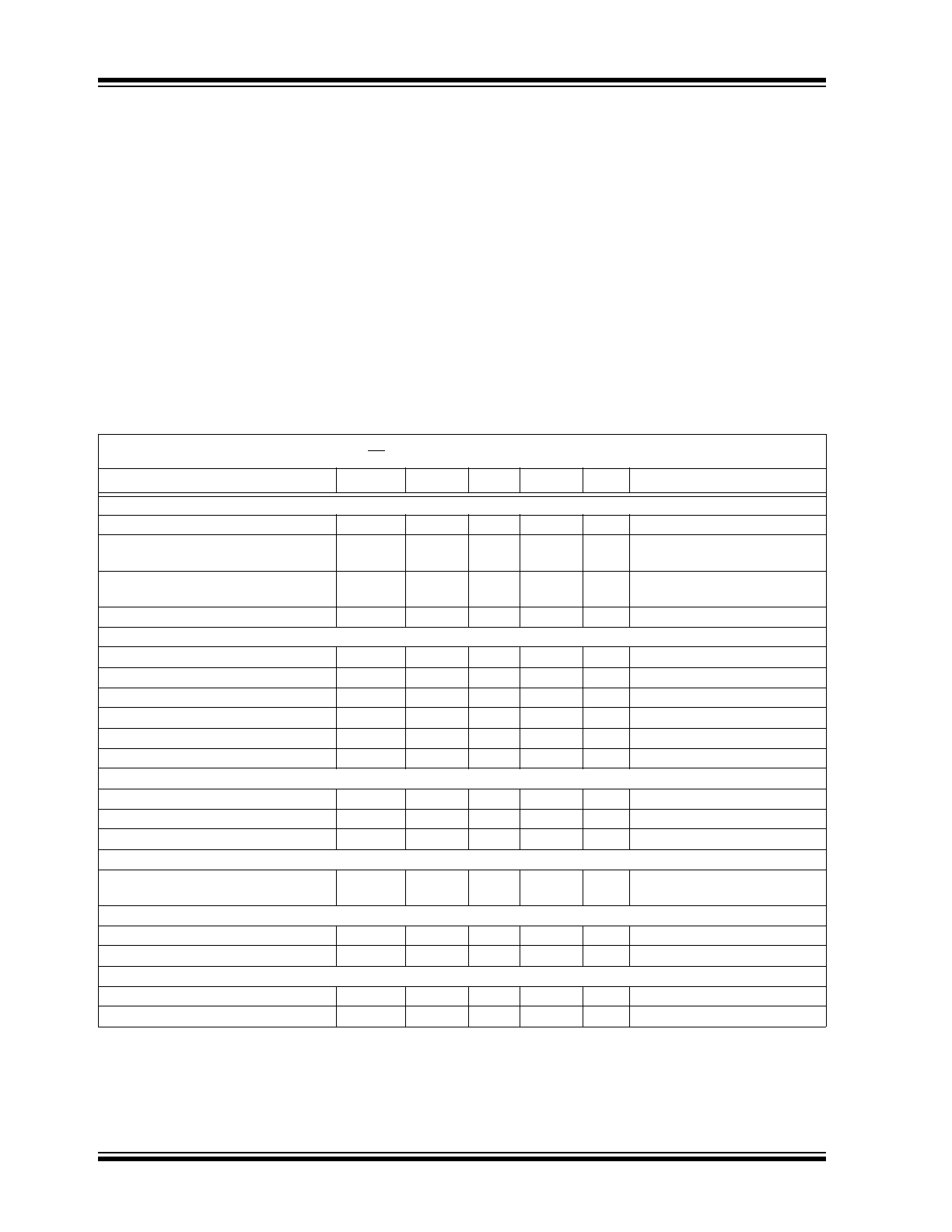
FIGURE 1-1:
Timing Diagram for the Chip
Select (CS) pin on the MCP6283 and MCP6285.
Electrical Characteristics: Unless otherwise indicated, T
A
= +25°C, V
DD
= +2.2V to +5.5V, V
SS
= GND, V
OUT
≈ V
DD
/2,
V
CM
= V
DD
/2, V
L
= V
DD
/2, R
L
= 10 k
Ω to V
L
, C
L
= 60 pF and CS is tied low. (refer to
Figure 1-2
and
Figure 1-3
).
Parameters
Sym
Min
Typ
Max
Units
Conditions
AC Response
Gain Bandwidth Product
GBWP
—
5.0
—
MHz
Phase Margin at Unity-Gain
PM
—
65
—
°
G = +1 V/V
Slew Rate
SR
—
2.5
—
V/µs
Noise
Input Noise Voltage
E
ni
—
5.2
—
µV
P-P
f = 0.1 Hz to 10 Hz
Input Noise Voltage Density
e
ni
—
16
—
nV/
√Hz
f = 1 kHz
Input Noise Current Density
i
ni
—
3
—
fA/
√Hz
f = 1 kHz
Electrical Characteristics: Unless otherwise indicated, T
A
= +25°C, V
DD
= +2.2V to +5.5V, V
SS
= GND, V
OUT
≈ V
DD
/2,
V
CM
= V
DD
/2, V
L
= V
DD
/2, R
L
= 10 k
Ω to V
L
, C
L
= 60 pF and CS is tied low. (refer to
Figure 1-2
and
Figure 1-3
).
Parameters
Sym
Min
Typ
Max
Units
Conditions
CS Low Specifications
CS Logic Threshold, Low
V
IL
V
SS
—
0.2 V
DD
V
CS Input Current, Low
I
CSL
—
0.01
—
µA
CS = V
SS
CS High Specifications
CS Logic Threshold, High
V
IH
0.8 V
DD
—
V
DD
V
CS Input Current, High
I
CSH
—
0.7
2
µA
CS = V
DD
GND Current per Amplifier
I
SS
—
-0.7
—
µA
CS = V
DD
Amplifier Output Leakage
—
—
0.01
—
µA
CS = V
DD
Dynamic Specifications (Note 1)
CS Low to Valid Amplifier
Output, Turn-on Time
t
ON
—
4
10
µs
CS Low
≤ 0.2 V
DD
, G = +1 V/V,
V
IN
= V
DD
/2, V
OUT
= 0.9 V
DD
/2,
V
DD
= 5.0V
CS High to Amplifier Output High-Z
t
OFF
—
0.01
—
µs
CS High
≥ 0.8 V
DD
, G = +1 V/V,
V
IN
= V
DD
/2, V
OUT
= 0.1 V
DD
/2
Hysteresis
V
HYST
—
0.6
—
V
V
DD
= 5V
Note
1:
The input condition (V
IN
) specified applies to both op amp A and B of the MCP6285. The dynamic specification is tested
at the output of op amp B (V
OUTB
).
V
IL
Hi-Z
t
ON
V
IH
CS
t
OFF
V
OUT
-0.7 µA
Hi-Z
I
SS
I
CS
0.7 µA
0.7 µA
-0.7 µA
-450 µA
10 nA
(typical)
(typical)
(typical)
(typical)
(typical)
(typical)
MCP6281/1R/2/3/4/5
DS21811E-page 4
© 2008 Microchip Technology Inc.
TEMPERATURE SPECIFICATIONS
1.1
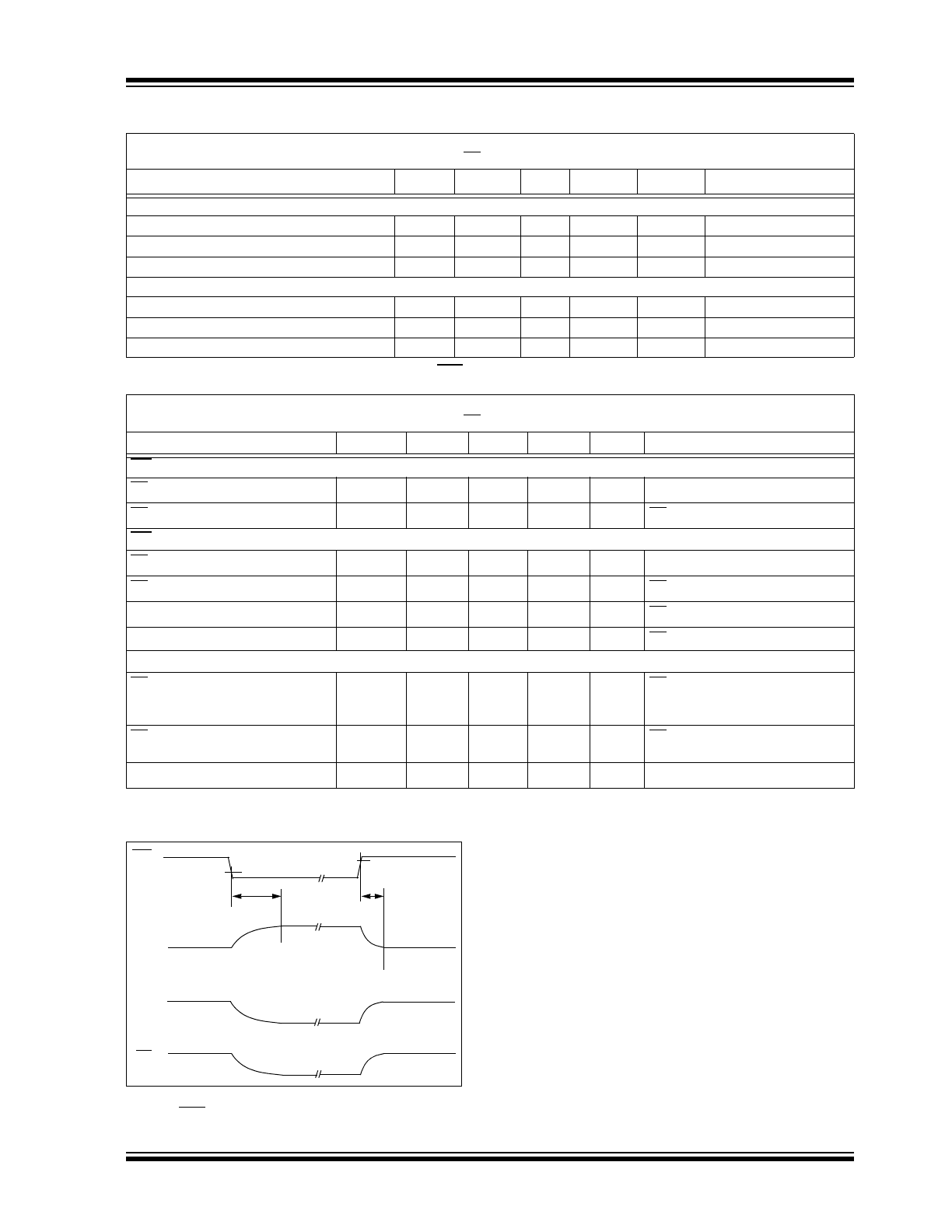
Test Circuits
The test circuits used for the DC and AC tests are
shown in
Figure 1-2
and
Figure 1-2
. The bypass
capacitors are laid out according to the rules discussed
in Section 4.6 “Supply Bypass”.
FIGURE 1-2:
AC and DC Test Circuit for
Most Non-Inverting Gain Conditions.
FIGURE 1-3:
AC and DC Test Circuit for
Most Inverting Gain Conditions.
Electrical Characteristics: Unless otherwise indicated, V
DD
= +2.2V to +5.5V and V
SS
= GND.
Parameters
Sym
Min
Typ
Max
Units
Conditions
Temperature Ranges
Operating Temperature Range
T
A
-40
—
+125
°C
Note
Storage Temperature Range
T
A
-65
—
+150
°C
Thermal Package Resistances
Thermal Resistance, 5L-SOT-23
θ
JA
—
256
—
°C/W
Thermal Resistance, 6L-SOT-23
θ
JA
—
230
—
°C/W
Thermal Resistance, 8L-PDIP
θ
JA
—
85
—
°C/W
Thermal Resistance, 8L-SOIC
θ
JA
—
163
—
°C/W
Thermal Resistance, 8L-MSOP
θ
JA
—
206
—
°C/W
Thermal Resistance, 14L-PDIP
θ
JA
—
70
—
°C/W
Thermal Resistance, 14L-SOIC
θ
JA
—
120
—
°C/W
Thermal Resistance, 14L-TSSOP
θ
JA
—
100
—
°C/W
Note:
The Junction Temperature (T
J
) must not exceed the Absolute Maximum specification of +150°C.
V
DD
MCP628X
R
G
R
F
R
N
V
OUT
V
IN
V
DD
/2
1 µF
C
L
R
L
V
L
0.1 µF
V
DD
MCP628X
R
G
R
F
R
N
V
OUT
V
DD
/2
V
IN
1 µF
C
L
R
L
V
L
0.1 µF
© 2008 Microchip Technology Inc.
DS21811E-page 5
MCP6281/1R/2/3/4/5
2.0
TYPICAL PERFORMANCE CURVES
Note: Unless otherwise indicated, T
A
= +25°C, V
DD
= +2.2V to +6.0V, V
SS
= GND, V
CM
= V
DD
/2, V
OUT
≈ V
DD
/2,
V
L
= V
DD
/2, R
L
= 10 k
Ω to V
L
, C
L
= 60 pF and CS is tied low.
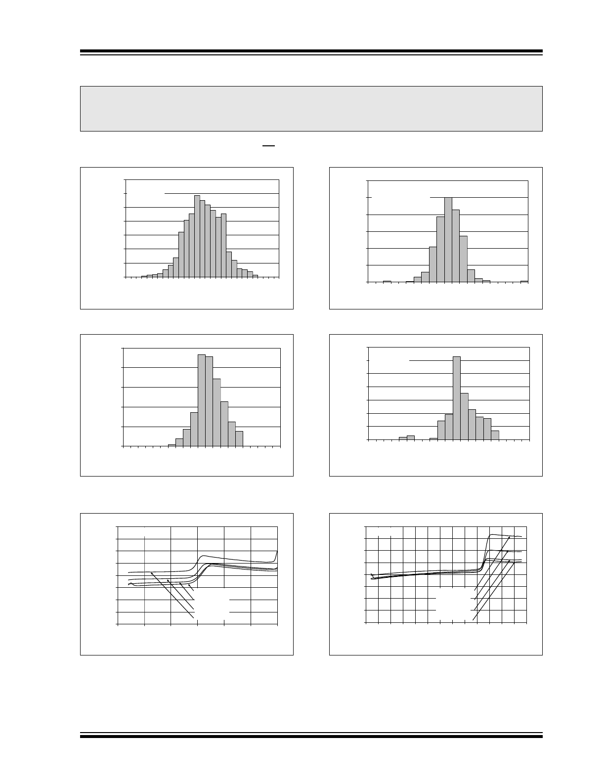
FIGURE 2-1:
Input Offset Voltage.
FIGURE 2-2:
Input Bias Current at
T
A
= +85 °C.
FIGURE 2-3:
Input Offset Voltage vs.
Common Mode Input Voltage at V
DD
= 2.2V.
FIGURE 2-4:
Input Offset Voltage Drift.
FIGURE 2-5:
Input Bias Current at
T
A
= +125 °C.
FIGURE 2-6:
Input Offset Voltage vs.
Common Mode Input Voltage at V
DD
= 5.5V.
Note:
The graphs and tables provided following this note are a statistical summary based on a limited number of
samples and are provided for informational purposes only. The performance characteristics listed herein
are not tested or guaranteed. In some graphs or tables, the data presented may be outside the specified
operating range (e.g., outside specified power supply range) and therefore outside the warranted range.
0%
2%
4%
6%
8%
10%
12%
14%
-2.8
-2.4
-2.0
-1.6
-1.2
-0.8
-0.4
0.0
0.4
0.8
1.2
1.6
2.0
2.4
2.8
Input Offset Voltage (mV)
P
e
rcentage of O
ccur
re
nces
832 Samples
V
CM
= V
SS
0%
5%
10%
15%
20%
25%
0
10
20
30
40
50
60
70
80
90
100
Input Bias Current (pA)
Perce
n
tag
e
o
f
Occu
rren
ces
210 Samples
T
A
= +85°C
-100
-50
0
50
100
150
200
250
300
-0.5
0.0
0.5
1.0
1.5
2.0
2.5
Common Mode Input Voltage (V)
In
pu
t Of
fs
e
t V
o
lt
a
g
e
(
µ
V
)
V
DD
= 2.2V
T
A
= +125°C
T
A
= +85°C
T
A
= +25°C
T
A
= -40°C
0%
5%
10%
15%
20%
25%
30%
-10
-8
-6
-4
-2
0
2
4
6
8
10
Input Offset Voltage Drift (µV/°C)
P
e
rcentage of O
ccur
re
nces
832 Samples
V
CM
= V
SS
T
A
= -40°C to +125°C
0%
5%
10%
15%
20%
25%
30%
35%
0
20
0
40
0
80
0
120
0
160
0
200
0
240
0
280
0
320
0
360
0
Input Bias Current (pA)
Percen
tage
o
f
Occu
rren
ces
210 Samples
T
A
= +125°C
-100
-50
0
50
100
150
200
250
300
-0.5
0.
0
0.
5
1.
0
1.
5
2.
0
2.
5
3.
0
3.
5
4.
0
4.
5
5.
0
5.
5
6.
0
Common Mode Input Voltage (V)
In
pu
t Off
s
et Vol
ta
g
e
(µ
V)
V
DD
= 5.5V
T
A
= +125°C
T
A
= +85°C
T
A
= +25°C
T
A
= -40°C
MCP6281/1R/2/3/4/5
DS21811E-page 6
© 2008 Microchip Technology Inc.
TYPICAL PERFORMANCE CURVES
(CONTINUED)
Note: Unless otherwise indicated, T
A
= +25°C, V
DD
= +2.2V to +6.0V, V
SS
= GND, V
CM
= V
DD
/2, V
OUT
≈ V
DD
/2,
V
L
= V
DD
/2, R
L
= 10 k
Ω to V
L
, C
L
= 60 pF and CS is tied low.
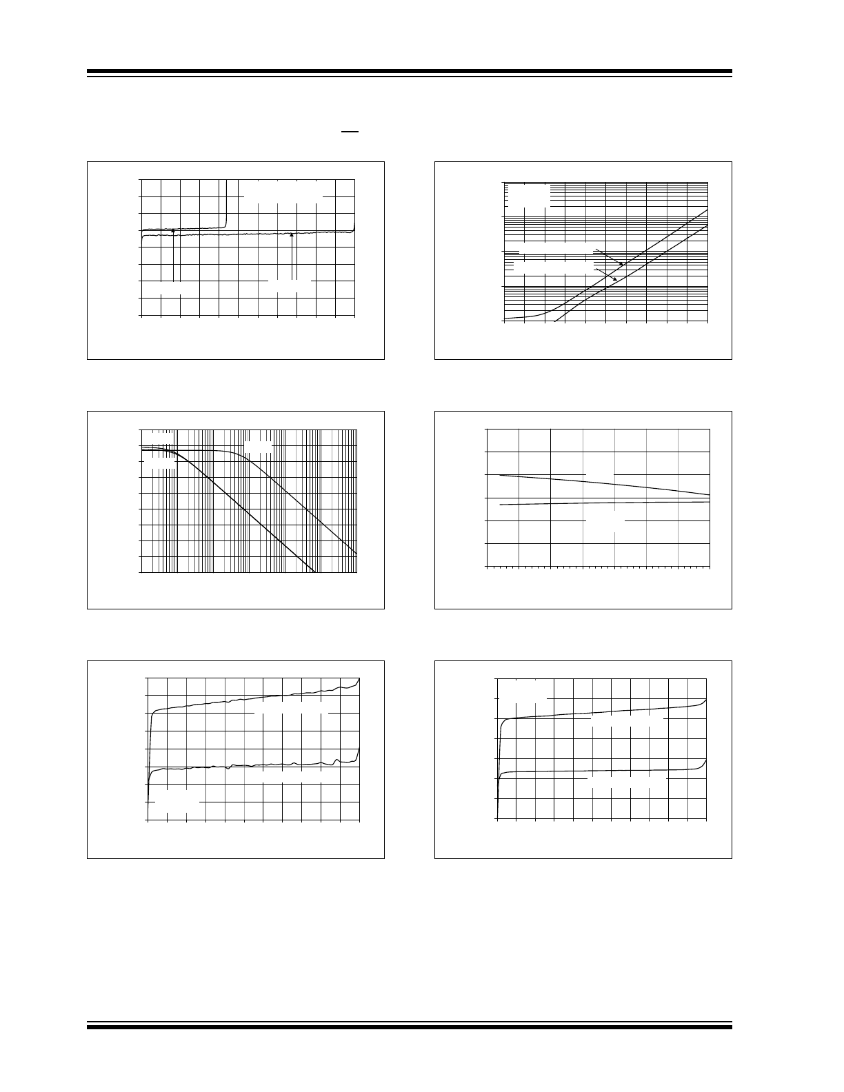
FIGURE 2-7:
Input Offset Voltage vs.
Output Voltage.
FIGURE 2-8:
CMRR, PSRR vs.
Frequency.
FIGURE 2-9:
Input Bias, Offset Currents
vs. Common Mode Input Voltage at T
A
= +85°C.
FIGURE 2-10:
Input Bias, Input Offset
Currents vs. Ambient Temperature.
FIGURE 2-11:
CMRR, PSRR vs. Ambient
Temperature.
FIGURE 2-12:
Input Bias, Offset Currents
vs. Common Mode Input Voltage at T
A
= +125°C.
-100
-50
0
50
100
150
200
250
300
0.0
0.5
1.0
1.5
2.0
2.5
3.0
3.5
4.0
4.5
5.0
5.5
Output Voltage (V)
Input Offset Voltage (µV)
V
DD
= 2.2V
V
CM
= V
SS
Representative Part
V
DD
= 5.5V
20
30
40
50
60
70
80
90
100
110
1.E+00
1.E+01
1.E+02
1.E+03
1.E+04
1.E+05
1.E+06
Frequency (Hz)
CM
R
R
, PSRR (
d
B)
1
10k
100k
1M
100
10
1k
PSRR+
PSRR-
CMRR
-25
-15
-5
5
15
25
35
45
55
0.0
0.5
1.0
1.5
2.0
2.5
3.0
3.5
4.0
4.5
5.0
5.5
Common Mode Input Voltage (V)
Input Bias, Offset Currents
(pA)
T
A
= +85°C
V
DD
= 5.5V
Input Bias Current
Input Offset Current
1
10
100
1,000
10,000
25
35
45
55
65
75
85
95
105 115 125
Ambient Temperature (°C)
Input Bias, Offset Currents
(pA)
Input Bias Current
Input Offset Current
V
CM
= V
DD
V
DD
= 5.5V
60
70
80
90
100
110
120
-50
-25
0
25
50
75
100
125
Ambient Temperature (°C)
P
S
R
R,
CM
RR
(
d
B)
PSRR
V
CM
= V
SS
CMRR
-1.0
-0.5
0.0
0.5
1.0
1.5
2.0
2.5
0.0
0.5
1.0
1.5
2.0
2.5
3.0
3.5
4.0
4.5
5.0
5.5
Common Mode Input Voltage (V)
In
p
u
t
Bi
as, Off
s
et
Cu
rren
ts
(n
A
)
T
A
= +125°C
V
DD
= 5.5V
Input Bias Current
Input Offset Current
© 2008 Microchip Technology Inc.
DS21811E-page 7
MCP6281/1R/2/3/4/5
TYPICAL PERFORMANCE CURVES
(CONTINUED)
Note: Unless otherwise indicated, T
A
= +25°C, V
DD
= +2.2V to +6.0V, V
SS
= GND, V
CM
= V
DD
/2, V
OUT
≈ V
DD
/2,
V
L
= V
DD
/2, R
L
= 10 k
Ω to V
L
, C
L
= 60 pF and CS is tied low.
FIGURE 2-13:
Quiescent Current vs.
Power Supply Voltage.
FIGURE 2-14:
Open-Loop Gain, Phase vs.
Frequency.
FIGURE 2-15:
Maximum Output Voltage
Swing vs. Frequency.
FIGURE 2-16:
Output Voltage Headroom
vs. Output Current Magnitude.
FIGURE 2-17:
Gain Bandwidth Product,
Phase Margin vs. Ambient Temperature.
FIGURE 2-18:
Slew Rate vs. Ambient
Temperature.
0
100
200
300
400
500
600
0.0
0.5
1.0
1.5
2.0
2.5
3.0
3.5
4.0
4.5
5.0
5.5
Power Supply Voltage (V)
Q
u
ie
scent Cur
re
nt
(µ
A/a
m
plif
ie
r)
T
A
= +125°C
T
A
= +85°C
T
A
= +25°C
T
A
= -40°C
-20
0
20
40
60
80
100
120
1.
E
-01
1.
E
+
00
1.
E
+
01
1.
E
+
02
1.
E
+
03
1.
E
+
04
1.
E
+
05
1.
E
+
06
1.
E
+
07
1.
E
+
08
Frequency (Hz)
Open-Loop Gain (dB)
-210
-180
-150
-120
-90
-60
-30
0
Open-Loop P
h
ase (°
)
Gain
Phase
0.1
1
10
100
1k
10k 100k 1M 10M 100M
0.1
1
10
1.
E
+
03
1.
E
+
04
1.
E
+
05
1.
E
+
06
1.
E
+
07
Frequency (Hz)
Maxi
m
u
m
O
u
tput V
o
lt
age
Swing (V
P-
P
)
V
DD
= 2.2V
1k
10k
100k
1M
V
DD
= 5.5V
10M
1
10
100
1000
0.01
0.1
1
10
Output Current Magnitude (mA)
Ouput Voltage Headroom (mV)
V
OL
- V
SS
V
DD
- V
OH
0
1
2
3
4
5
6
-50
-25
0
25
50
75
100
125
Ambient Temperature (°C)
G
a
in
B
a
nd
w
id
th
Pr
o
duc
t
(M
H
z
)
60
65
70
75
80
85
90
Pha
se Marg
in
(°)
Gain Bandwidth Product
V
DD
= 5.5V
V
DD
= 2.2V
V
DD
= 2.2V
V
DD
= 5.5V
Phase Margin
0.0
0.5
1.0
1.5
2.0
2.5
3.0
3.5
4.0
4.5
-50
-25
0
25
50
75
100
125
Ambient Temperature (°C)
S
le
w
R
a
te
(V
/µ
s)
Rising Edge, V
DD
= 2.2V
Rising Edge, V
DD
= 5.5V
Falling Edge, V
DD
= 5.5V
Falling Edge, V
DD
= 2.2V
MCP6281/1R/2/3/4/5
DS21811E-page 8
© 2008 Microchip Technology Inc.
TYPICAL PERFORMANCE CURVES
(CONTINUED)
Note: Unless otherwise indicated, T
A
= +25°C, V
DD
= +2.2V to +6.0V, V
SS
= GND, V
CM
= V
DD
/2, V
OUT
≈ V
DD
/2,
V
L
= V
DD
/2, R
L
= 10 k
Ω to V
L
, C
L
= 60 pF and CS is tied low.
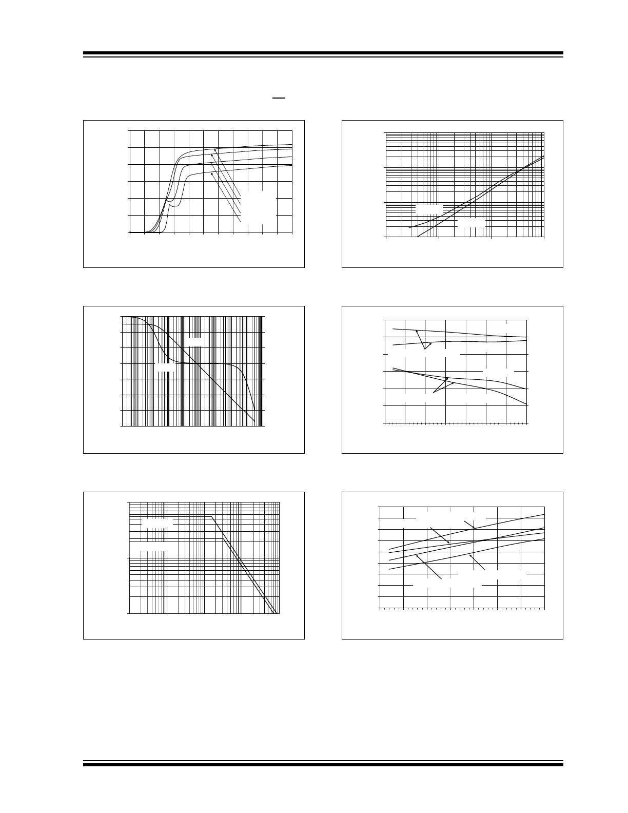
FIGURE 2-19:
Input Noise Voltage Density
vs. Frequency.
FIGURE 2-20:
Output Short Circuit Current
vs. Power Supply Voltage.
FIGURE 2-21:
Quiescent Current vs.
Chip Select (CS) Voltage at V
DD
= 2.2V
(MCP6283 and MCP6285 only).
FIGURE 2-22:
Input Noise Voltage Density
vs. Common Mode Input Voltage at 1 kHz.
FIGURE 2-23:
Channel-to-Channel
Separation vs. Frequency (MCP6282 and
MCP6284 only).
FIGURE 2-24:
Quiescent Current vs.
Chip Select (CS) Voltage at V
DD
= 5.5V
(MCP6283 and MCP6285 only).
10
100
1,000
1.E-01
1.E+00
1.E+01
1.E+02
1.E+03
1.E+04
1.E+05
1.E+06
Frequency (Hz)
Input
Nois
e
Volt
ag
e D
e
ns
it
y
(nV
/√
Hz)
0.1
100
10
1k
100k
10k
1M
1
0
5
10
15
20
25
30
35
0.0
0.5
1.0
1.5
2.0
2.5
3.0
3.5
4.0
4.5
5.0
5.5
Power Supply Voltage (V)
Ouptut Short Circuit Current
(mA)
T
A
= +125°C
T
A
= +85°C
T
A
= +25°C
T
A
= -40°C
0
50
100
150
200
250
300
350
400
450
500
0.0
0.2
0.4
0.6
0.8
1.0
1.2
1.4
1.6
1.8
2.0
2.2
Chip Select Voltage (V)
Q
u
iescent Curr
ent
(µ
A/Ampl
ifier)
Hysteresis
Op-Amp shuts off here
Op-Amp turns on here
V
DD
= 2.2V
CS swept
high to low
CS swept
low to high
0
5
10
15
20
25
30
0.0
0.5
1.0
1.5
2.0
2.5
3.0
3.5
4.0
4.5
5.0
Common Mode Input Voltage (V)
Input Noise V
o
ltage Dens
ity
(n
V/
√Hz
)
f = 1 kHz
V
DD
= 5.0V
100
110
120
130
140
1
10
100
Frequency (kHz)
Channel-to-Channel Separation
(dB)
0
100
200
300
400
500
600
700
800
900
1000
0.0
0.5
1.0
1.5
2.0
2.5
3.0
3.5
4.0
4.5
5.0
5.5
Chip Select Voltage (V)
Q
u
iesc
ent C
u
rrent
(µ
A/Am
plif
ie
r)
Hysteresis
Op Amp toggles On/Off here
V
DD
= 5.5V
CS swept
low to high
CS
sw
ept
hi
gh to low
© 2008 Microchip Technology Inc.
DS21811E-page 9
MCP6281/1R/2/3/4/5
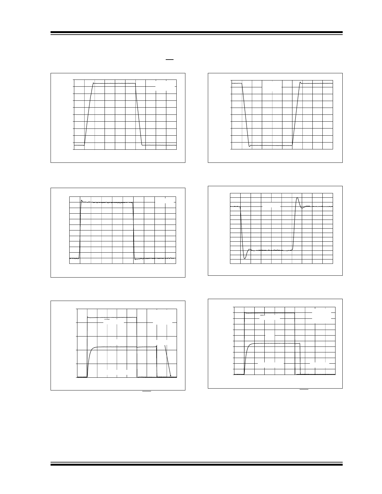
TYPICAL PERFORMANCE CURVES
(CONTINUED)
Note: Unless otherwise indicated, T
A
= +25°C, V
DD
= +2.2V to +6.0V, V
SS
= GND, V
CM
= V
DD
/2, V
OUT
≈ V
DD
/2,
V
L
= V
DD
/2, R
L
= 10 k
Ω to V
L
, C
L
= 60 pF and CS is tied low.
FIGURE 2-25:
Large-Signal, Non-inverting
Pulse Response.
FIGURE 2-26:
Small-Signal, Non-inverting
Pulse Response.
FIGURE 2-27:
Chip Select (CS) to
Amplifier Output Response Time at V
DD
= 2.2V
(MCP6283 and MCP6285 only).
FIGURE 2-28:
Large-Signal, Inverting
Pulse Response.
FIGURE 2-29:
Small-Signal, Inverting
Pulse Response.
FIGURE 2-30:
Chip Select (CS) to
Amplifier Output Response Time at V
DD
= 5.5V
(MCP6283 and MCP6285 only).
0.0
0.5
1.0
1.5
2.0
2.5
3.0
3.5
4.0
4.5
5.0
0.E+00
2.E-06
4.E-06
6.E-06
8.E-06
1.E-05
1.E-05
1.E-05
2.E-05
2.E-05
2.E-05
Time (2 µs/div)
Output Vol
tage (V)
G = +1V/V
V
DD
= 5.0V
Time (500 ns/div)
Output Voltage (10 mV/div)
G = +1V/V
0.0
0.5
1.0
1.5
2.0
2.5
0.0E+00
5.0E-06
1.0E-05
1.5E-05
2.0E-05
2.5E-05
3.0E-05
3.5E-05
4.0E-05
4.5E-05
5.0E-05
Time (5 µs/div)
C
h
ip Selec
t, O
u
tp
ut V
o
lta
g
es
(V
)
V
OUT
Output On
Output High-Z
V
DD
= 2.2V
G = +1V/V
V
IN
= V
SS
CS Voltage
0.0
0.5
1.0
1.5
2.0
2.5
3.0
3.5
4.0
4.5
5.0
0.E+00
2.E-06
4.E-06
6.E-06
8.E-06
1.E-05
1.E-05
1.E-05
2.E-05
2.E-05
2.E-05
Time (2 µs/div)
Output Voltage (V)
G = -1V/V
V
DD
= 5.0V
Time (500 ns/div)
O
u
tput V
o
lt
age (10 mV
/d
iv
)
G = -1V/V
0.0
0.5
1.0
1.5
2.0
2.5
3.0
3.5
4.0
4.5
5.0
5.5
6.0
0.E+00
5.E-06
1.E-05
2.E-05
2.E-05
3.E-05
3.E-05
4.E-05
4.E-05
5.E-05
5.E-05
Time (5 µs/div)
C
h
ip Sele
ct, Out
p
ut
V
o
lt
ages
(V)
V
OUT
Output On
Output High-Z
V
DD
= 5.5V
G = +1V/V
V
IN
= V
SS
CS Voltage
MCP6281/1R/2/3/4/5
DS21811E-page 10
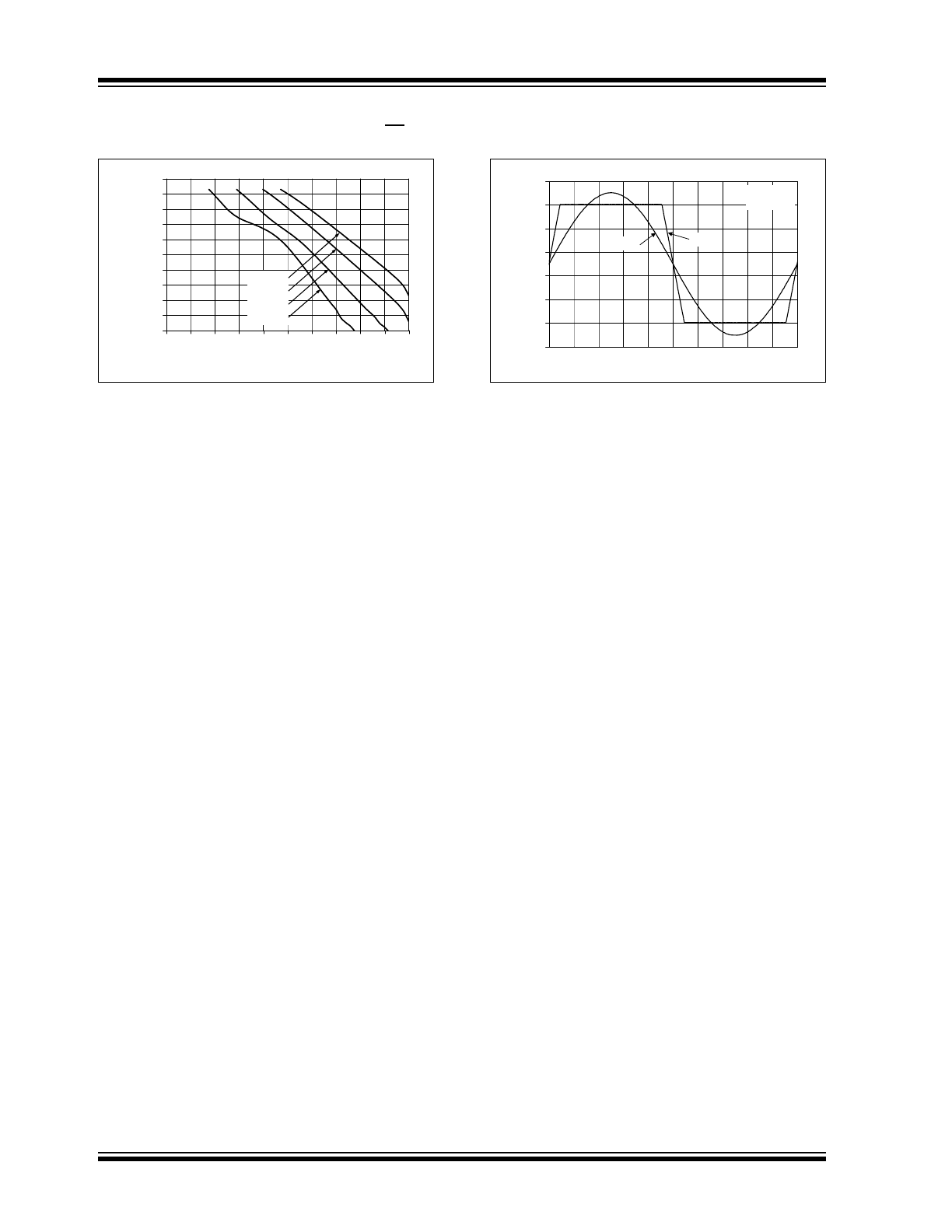
© 2008 Microchip Technology Inc.
Note: Unless otherwise indicated, T
A
= +25°C, V
DD
= +2.2V to +6.0V, V
SS
= GND, V
CM
= V
DD
/2, V
OUT
≈ V
DD
/2,
V
L
= V
DD
/2, R
L
= 10 k
Ω to V
L
, C
L
= 60 pF and CS is tied low.
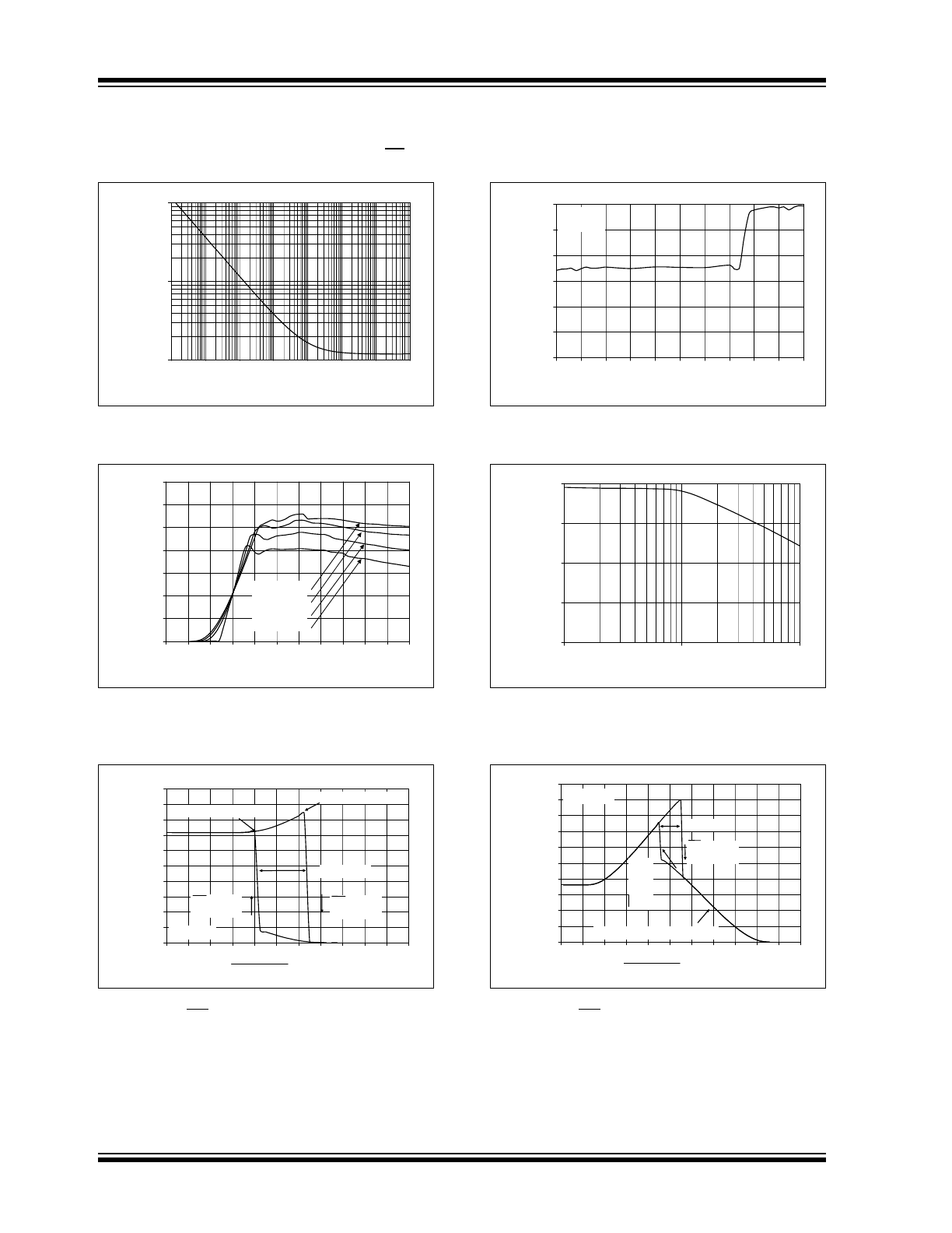
FIGURE 2-31:
Measured Input Current vs.
Input Voltage (below V
SS
).
FIGURE 2-32:
The MCP6281/1R/2/3/4/5
Show No Phase Reversal.
1.E-12
1.E-11
1.E-10
1.E-09
1.E-08
1.E-07
1.E-06
1.E-05
1.E-04
1.E-03
1.E-02
-1.0 -0.9 -0.8 -0.7 -0.6 -0.5 -0.4 -0.3 -0.2 -0.1 0.0
Input Voltage (V)
In
put
C
u
rr
e
n
t Ma
gn
it
u
d
e
(A
)
+125°C
+85°C
+25°C
-40°C
10m
1m
100µ
10µ
1µ
100n
10n
1n
100p
10p
1p
-1
0
1
2
3
4
5
6
-15
-14
-13
-12
-11
-10
-9
-8
-7
-6
-5
Time (1 ms/div)
Input, Output Voltage (V)
V
DD
= 5.0V
G = +2 V/V
V
IN
V
OUT