

Features
•
High Performance, Low Power AVR ® 8-bit Microcontroller
•
Advanced RISC Architecture
– 131 Powerful Instructions - Most Single Clock Cycle Execution
– 32 x 8 General Purpose Working Registers
– Fully Static Operation
– Up to 1 MIPS throughput per MHz
– On-chip 2-cycle Multiplier
•
Data and Non-Volatile Program Memory
– 8K Bytes Flash of In-System Programmable Program Memory
• Endurance: 10,000 Write/Erase Cycles
– Optional Boot Code Section with Independent Lock Bits
•
In-System Programming by On-chip Boot Program
•
True Read-While-Write Operation
– 512 Bytes of In-System Programmable EEPROM
•
Endurance: 100,000 Write/Erase Cycles
– 512 Bytes Internal SRAM
– Programming Lock for Flash Program and EEPROM Data Security
•
On Chip Debug Interface (debugWIRE)
•
Peripheral Features
– Two 12-bit High Speed PSC (Power Stage Controllers) with 4-bit Resolution
Enhancement
• Non Overlapping Inverted PWM Output Pins With Flexible Dead-Time
• Variable PWM duty Cycle and Frequency
• Synchronous Update of all PWM Registers
• Auto Stop Function for Event Driven PFC Implementation
• Less than 25 Hz Step Width at 150 kHz Output Frequency
• PSC2 with four Output Pins and Output Matrix
– One 8-bit General purpose Timer/Counter with Separate Prescaler and Capture
Mode
– One 16-bit General purpose Timer/Counter with Separate Prescaler, Compare
Mode and Capture Mode
– Master/Slave SPI Serial Interface
– 10-bit ADC
• 8 Single Ended Channels and 1 Fully Differential ADC Channel Pair
• Programmable Gain (5x, 10x, 20x, 40x on Differential Channel)
• Internal Reference Voltage
– Two Analog Comparator with Resistor-Array to Adjust Comparison Voltage
– 4 External Interrupts
– Programmable Watchdog Timer with Separate On-Chip Oscillator
•
Special Microcontroller Features
– Low Power Idle, Noise Reduction, and Power Down Modes
– Power On Reset and Programmable Brown Out Detection
– Flag Array in Bit-programmable I/O Space (4 bytes)
– In-System Programmable via SPI Port
– Internal Calibrated RC Oscillator ( 8 MHz)
– On-chip PLL for fast PWM ( 32 MHz, 64 MHz) and CPU (16 MHz)
4378CS–AVR–09/08
8-bit
Microcontroller
with 8K Bytes
In-System
Programmable
Flash
AT90PWM1
Summary
2
4378CS–AVR–09/08
AT90PWM1
•
Operating Voltage: 2.7V - 5.5V
•
Extended Operating Temperature:
– -40°C to +105°
1.
History
2.
Disclaimer
Typical values contained in this datasheet are based on simulations and characterization of
other AVR microcontrollers manufactured on the same process technology. Min and Max val-
ues will be available after the device is characterized.
3.
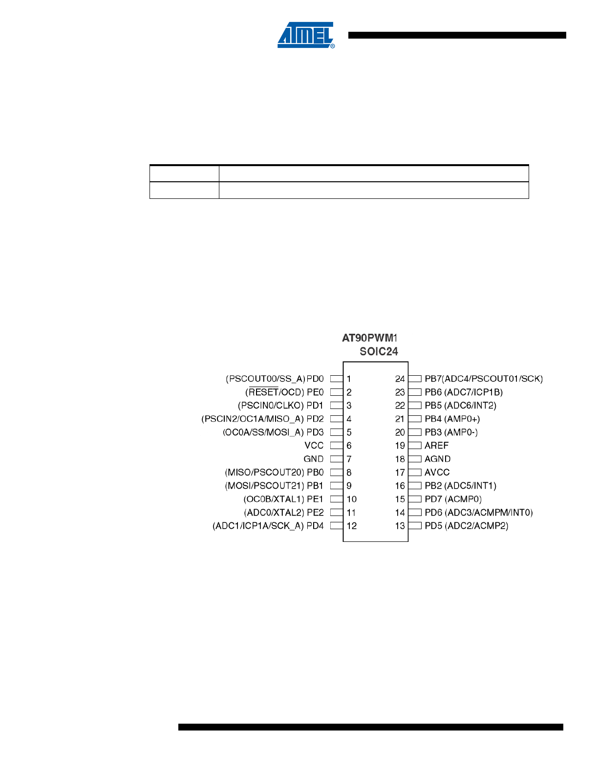
Pin Configurations
Figure 3-1.
SOIC 24-pin Package
Product
Revision
AT90PWM1
First revision of parts

3
4378CS–AVR–09/08
AT90PWM1
Figure 3-2.
QFN 32 -pin Package
1
2
3
4
5
6
7
8
24
23
22
21
20
19
18
17
(PSCIN2/OC1A/MISO_A) PD2
(OC0A/SS/MOSI_A) PD3
NC
VCC
GND
NC
NC
(MISO/PSCOUT20) PB0
PB4 (AMP0+)
PB3 (AMP0-)
NC
AREF
AGND
AVCC
NC
NC
32
31
30
29
28
27
26
25
9
10
11
12
13
14
15
16
(MOSI/PSCOUT21) PB1
(OC0B/XT
AL1) PE1
(ADC0/XT
AL2) PE2
(ADC1/ICP1_A/SCK_A) PD4
(ADC2/ACMP2 ) PD5
(ADC3/ACMPM/INT0) PD6
(ACMP0) PD7
(ADC5/INT1) PB2
PD1
(PSCIN0/CLKO)
PE0
(RESET/OCD)
NC
PD0
(PSCOUT00/SS_A)
PB7 (ADC4/PSCOUT01/SCK)
PB6 (ADC7/ICP1B)
PB5 (ADC6/INT2)
NC
AT90PWM1 QFN 32

4
4378CS–AVR–09/08
AT90PWM1
3.1
Pin Descriptions
Table 3-1.
Pin out description
QFN32
S024 Pin Number
Mnemonic
Type
Name, Function & Alternate Function
5
7
GND
Power
Ground: 0V reference
20
18
AGND
Power
Analog Ground: 0V reference for analog part
4
6
VCC
power
Power Supply:
19
17
AVCC
Power
Analog Power Supply: This is the power supply voltage for analog
part
For a normal use this pin must be connected.
21
19
AREF
Power
Analog Reference : reference for analog converter . This is the
reference voltage of the A/D converter. As output, can be used by
external analog
8
8
PBO
I/O
MISO (SPI Master In Slave Out)
PSCOUT20 output
9
9
PB1
I/O
MOSI (SPI Master Out Slave In)
PSCOUT21 output
16
16
PB2
I/O
ADC5 (Analog Input Channel5 )
INT1
23
20
PB3
I/O
AMP0- (Analog Differential Amplifier 0 Input Channel )
24
21
PB4
I/O
AMP0+ (Analog Differential Amplifier 0 Input Channel )
26
22
PB5
I/O
ADC6 (Analog Input Channel 6)
INT 2
27
23
PB6
I/O
ADC7 (Analog Input Channel 7)
ICP1B (Timer 1 input capture alternate input)
PSCOUT11 output
28
24
PB7
I/O
PSCOUT01 output
ADC4 (Analog Input Channel 4)
SCK (SPI Clock)
29
1
PD0
I/O
PSCOUT00 output
XCK (UART Transfer Clock)
SS_A (Alternate SPI Slave Select)
32
3
PD1
I/O
PSCIN0 (PSC 0 Digital Input )
CLKO (System Clock Output)
1
4
PD2
I/O
PSCIN2 (PSC 2 Digital Input)
OC1A (Timer 1 Output Compare A)
MISO_A (Programming & alternate SPI Master In Slave Out)
2
5
PD3
I/O
TXD (Dali/UART Tx data)
OC0A (Timer 0 Output Compare A)
SS (SPI Slave Select)
MOSI_A (Programming & alternate Master Out SPI Slave In)

5
4378CS–AVR–09/08
AT90PWM1
4.
Overview
The AT90PWM1 is a low-power CMOS 8-bit microcontroller based on the AVR enhanced RISC
architecture. By executing powerful instructions in a single clock cycle, the AT90PWM1 achieves
throughputs approaching 1 MIPS per MHz allowing the system designer to optimize power con-
sumption versus processing speed.
12
12
PD4
I/O
ADC1 (Analog Input Channel 1)
RXD (Dali/UART Rx data)
ICP1A (Timer 1 input capture)
SCK_A (Programming & alternate SPI Clock)
13
13
PD5
I/O
ADC2 (Analog Input Channel 2)
ACMP2 (Analog Comparator 2 Positive Input )
14
14
PD6
I/O
ADC3 (Analog Input Channel 3 )
ACMPM reference for analog comparators
INT0
15
15
PD7
I/O
ACMP0 (Analog Comparator 0 Positive Input )
31
2
PE0
I/O or I
RESET (Reset Input)
OCD (On Chip Debug I/O)
10
10
PE1
I/O
XTAL1: XTAL Input
OC0B (Timer 0 Output Compare B)
11
11
PE2
I/O
XTAL2: XTAL OuTput
ADC0 (Analog Input Channel 0)
Table 3-1.
Pin out description (Continued)
QFN32
S024 Pin Number
Mnemonic
Type
Name, Function & Alternate Function
6
4378CS–AVR–09/08
AT90PWM1
4.1
Block Diagram
Figure 4-1.
Block Diagram
The AVR core combines a rich instruction set with 32 general purpose working registers. All the
32 registers are directly connected to the Arithmetic Logic Unit (ALU), allowing two independent
registers to be accessed in one single instruction executed in one clock cycle. The resulting
architecture is more code efficient while achieving throughputs up to ten times faster than con-
ventional CISC microcontrollers.
The AT90PWM1 provides the following features: 8K bytes of In-System Programmable Flash
with Read-While-Write capabilities, 512 bytes EEPROM, 512 bytes SRAM, 53 general purpose
I/O lines, 32 general purpose working registers, 2 Power Stage Controllers, two flexible
Timer/Counters with compare modes and PWM, an 8-channel 10-bit ADC with two differential

7
4378CS–AVR–09/08
AT90PWM1
input stage with programmable gain, a programmable Watchdog Timer with Internal Oscillator,
an SPI serial port, an On-chip Debug system and four software selectable power saving modes.
The Idle mode stops the CPU while allowing the SRAM, Timer/Counters, SPI ports and interrupt
system to continue functioning. The Power-down mode saves the register contents but freezes
the Oscillator, disabling all other chip functions until the next interrupt or Hardware Reset. The
ADC Noise Reduction mode stops the CPU and all I/O modules except ADC, to minimize switch-
ing noise during ADC conversions. In Standby mode, the Crystal/Resonator Oscillator is running
while the rest of the device is sleeping. This allows very fast start-up combined with low power
consumption.
The device is manufactured using Atmel’s high-density nonvolatile memory technology. The On-
chip ISP Flash allows the program memory to be reprogrammed in-system through an SPI serial
interface, by a conventional nonvolatile memory programmer, or by an On-chip Boot program
running on the AVR core. The boot program can use any interface to download the application
program in the application Flash memory. Software in the Boot Flash section will continue to run
while the Application Flash section is updated, providing true Read-While-Write operation. By
combining an 8-bit RISC CPU with In-System Self-Programmable Flash on a monolithic chip,
the Atmel AT90PWM1 is a powerful microcontroller that provides a highly flexible and cost effec-
tive solution to many embedded control applications.
The AT90PWM1 AVR is supported with a full suite of program and system development tools
including: C compilers, macro assemblers, program debugger/simulators, in-circuit emulators,
and evaluation kits.
4.2
Pin Descriptions
4.2.1
VCC
Digital supply voltage.
4.2.2
GND
Ground.
4.2.3
Port B (PB7..PB0)
Port B is an 8-bit bi-directional I/O port with internal pull-up resistors (selected for each bit). The
Port B output buffers have symmetrical drive characteristics with both high sink and source
capability. As inputs, Port B pins that are externally pulled low will source current if the pull-up
resistors are activated. The Port B pins are tri-stated when a reset condition becomes active,
even if the clock is not running.
Port B also serves the functions of various special features of the AT90PWM1 as listed on
page
65
.
4.2.4
Port D (PD7..PD0)
Port D is an 8-bit bi-directional I/O port with internal pull-up resistors (selected for each bit). The
Port D output buffers have symmetrical drive characteristics with both high sink and source
capability. As inputs, Port D pins that are externally pulled low will source current if the pull-up
resistors are activated. The Port D pins are tri-stated when a reset condition becomes active,
even if the clock is not running.
Port D also serves the functions of various special features of the AT90PWM1 as listed on
page
68
.

8
4378CS–AVR–09/08
AT90PWM1
4.2.5
Port E (PE2..0) RESET/ XTAL1/
XTAL2
Port E is an 3-bit bi-directional I/O port with internal pull-up resistors (selected for each bit). The
Port E output buffers have symmetrical drive characteristics with both high sink and source
capability. As inputs, Port E pins that are externally pulled low will source current if the pull-up
resistors are activated. The Port E pins are tri-stated when a reset condition becomes active,
even if the clock is not running.
If the RSTDISBL Fuse is programmed, PE0 is used as an I/O pin. Note that the electrical char-
acteristics of PE0 differ from those of the other pins of Port C.
If the RSTDISBL Fuse is unprogrammed, PE0 is used as a Reset input. A low level on this pin
for longer than the minimum pulse length will generate a Reset, even if the clock is not running.
The minimum pulse length is given in
Table 9-1 on page 43
. Shorter pulses are not guaranteed
to generate a Reset.
Depending on the clock selection fuse settings, PE1 can be used as input to the inverting Oscil-
lator amplifier and input to the internal clock operating circuit.
Depending on the clock selection fuse settings, PE2 can be used as output from the inverting
Oscillator amplifier.
The various special features of Port E are elaborated in
“Alternate Functions of Port E” on page
71
and
“Clock Systems and their Distribution” on page 27
.
4.2.6
AVCC
AVCC is the supply voltage pin for the A/D Converter on Port F. It should be externally con-
nected to V
CC
, even if the ADC is not used. If the ADC is used, it should be connected to V
CC
through a low-pass filter.
4.2.7
AREF
This is the analog reference pin for the A/D Converter.
4.3
About Code Examples
This documentation contains simple code examples that briefly show how to use various parts of
the device. These code examples assume that the part specific header file is included before
compilation. Be aware that not all C compiler vendors include bit definitions in the header files
and interrupt handling in C is compiler dependent. Please confirm with the C compiler documen-
tation for more details.
9
4378CS–AVR–09/08
AT90PWM1
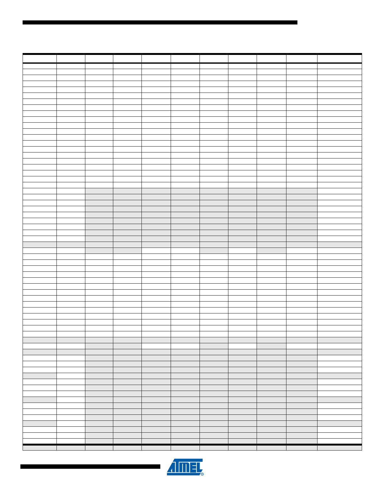
5.
Register Summary
Address
Name
Bit 7
Bit 6
Bit 5
Bit 4
Bit 3
Bit 2
Bit 1
Bit 0
Page
(0xFF)
PICR2H
page 162
(0xFE)
PICR2L
page 162
(0xFD)
PFRC2B
PCAE2B
PISEL2B
PELEV2B
PFLTE2B
PRFM2B3
PRFM2B2
PRFM2B1
PRFM2B0
page 161
(0xFC)
PFRC2A
PCAE2A
PISEL2A
PELEV2A
PFLTE2A
PRFM2A3
PRFM2A2
PRFM2A1
PRFM2A0
page 161
(0xFB)
PCTL2
PPRE21
PPRE20
PBFM2
PAOC2B
PAOC2A
PARUN2
PCCYC2
PRUN2
page 160
(0xFA)
PCNF2
PFIFTY2
PALOCK2
PLOCK2
PMODE21
PMODE20
POP2
PCLKSEL2
POME2
page 157
(0xF9)
OCR2RBH
page 157
(0xF8)
OCR2RBL
page 157
(0xF7)
OCR2SBH
page 157
(0xF6)
OCR2SBL
page 157
(0xF5)
OCR2RAH
page 156
(0xF4)
OCR2RAL
page 156
(0xF3)
OCR2SAH
page 156
(0xF2)
OCR2SAL
page 156
(0xF1)
POM2
POMV2B3
POMV2B2
POMV2B1
POMV2B0
POMV2A3
POMV2A2
POMV2A1
POMV2A0
page 163
(0xF0)
PSOC2
POS23
POS22
PSYNC21
PSYNC20
POEN2D
POEN2B
POEN2C
POEN2A
page 155
(0xEF)
PICR1H
(0xEE)
PICR1L
(0xED)
PFRC1B
PCAE1B
PISEL1B
PELEV1B
PFLTE1B
PRFM1B3
PRFM1B2
PRFM1B1
PRFM1B0
page 161
(0xEC)
PFRC1A
PCAE1A
PISEL1A
PELEV1A
PFLTE1A
PRFM1A3
PRFM1A2
PRFM1A1
PRFM1A0
page 161
(0xEB)
PCTL1
PRUN1
page 160
(0xEA)
Reserved
–
–
–
–
–
–
–
–
(0xE9)
Reserved
–
–
–
–
–
–
–
–
(0xE8)
Reserved
–
–
–
–
–
–
–
–
(0xE7)
Reserved
–
–
–
–
–
–
–
–
(0xE6)
Reserved
–
–
–
–
–
–
–
–
(0xE5)
Reserved
–
–
–
–
–
–
–
–
(0xE4)
Reserved
–
–
–
–
–
–
–
–
(0xE3)
Reserved
–
–
–
–
–
–
–
–
(0xE2)
Reserved
–
–
–
–
–
–
–
–
(0xE1)
Reserved
–
–
–
–
–
–
–
–
(0xE0)
PSOC1
–
–
PSYNC11
PSYNC10
–
POEN1B
–
POEN1A
(0xDF)
PICR0H
page 162
(0xDE)
PICR0L
page 162
(0xDD)
PFRC0B
PCAE0B
PISEL0B
PELEV0B
PFLTE0B
PRFM0B3
PRFM0B2
PRFM0B1
PRFM0B0
page 161
(0xDC)
PFRC0A
PCAE0A
PISEL0A
PELEV0A
PFLTE0A
PRFM0A3
PRFM0A2
PRFM0A1
PRFM0A0
page 161
(0xDB)
PCTL0
PPRE01
PPRE00
PBFM0
PAOC0B
PAOC0A
PARUN0
PCCYC0
PRUN0
page 158
(0xDA)
PCNF0
PFIFTY0
PALOCK0
PLOCK0
PMODE01
PMODE00
POP0
PCLKSEL0
-
page 157
(0xD9)
OCR0RBH
page 157
(0xD8)
OCR0RBL
page 157
(0xD7)
OCR0SBH
page 157
(0xD6)
OCR0SBL
page 157
(0xD5)
OCR0RAH
page 156
(0xD4)
OCR0RAL
page 156
(0xD3)
OCR0SAH
page 156
(0xD2)
OCR0SAL
page 156
(0xD1)
Reserved
–
–
–
–
–
–
–
–
(0xD0)
PSOC0
–
–
PSYNC01
PSYNC00
–
POEN0B
–
POEN0A
page 155
(0xCF)
Reserved
–
–
–
–
–
–
–
–
(0xCE)
Reserved
–
–
–
–
–
–
–
–
(0xCD)
Reserved
–
–
–
–
–
–
–
–
(0xCC)
Reserved
–
–
–
–
–
–
–
–
(0xCB)
Reserved
–
–
–
–
–
–
–
–
(0xCA)
Reserved
–
–
–
–
–
–
–
–
(0xC9)
Reserved
–
–
–
–
–
–
–
–
(0xC8)
Reserved
–
–
–
–
–
–
–
–
(0xC7)
Reserved
–
–
–
–
–
–
–
–
(0xC6)
Reserved
–
–
–
–
–
–
–
–
(0xC5)
Reserved
–
–
–
–
–
–
–
–
(0xC4)
Reserved
–
–
–
–
–
–
–
–
(0xC3)
Reserved
–
–
–
–
–
–
–
–
(0xC2)
Reserved
–
–
–
–
–
–
–
–
(0xC1)
Reserved
–
–
–
–
–
–
–
–
(0xC0)
Reserved
–
–
–
–
–
–
–
–
(0xBF)
Reserved
–
–
–
–
–
–
–
–

10
4378CS–AVR–09/08
AT90PWM1
(0xBE)
Reserved
–
–
–
–
–
–
–
–
(0xBD)
Reserved
–
–
–
–
–
–
–
–
(0xBC)
Reserved
–
–
–
–
–
–
–
–
(0xBB)
Reserved
–
–
–
–
–
–
–
–
(0xBA)
Reserved
–
–
–
–
–
–
–
–
(0xB9)
Reserved
–
–
–
–
–
–
–
–
(0xB8)
Reserved
–
–
–
–
–
–
–
–
(0xB7)
Reserved
–
–
–
–
–
–
–
–
(0xB6)
Reserved
–
–
–
–
–
–
–
–
(0xB5)
Reserved
–
–
–
–
–
–
–
–
(0xB4)
Reserved
–
–
–
–
–
–
–
–
(0xB3)
Reserved
–
–
–
–
–
–
–
–
(0xB2)
Reserved
–
–
–
–
–
–
–
–
(0xB1)
Reserved
–
–
–
–
–
–
–
–
(0xB0)
Reserved
–
–
–
–
–
–
–
–
(0xAF)
AC2CON
AC2EN
AC2IE
AC2IS1
AC2IS0
AC2SADE-
AC2M2
AC2M1
AC2M0
page 178
(0xAD)
AC0CON
AC0EN
AC0IE
AC0IS1
AC0IS0
-
AC0M2
AC0M1
AC0M0
page 177
(0xAC)
Reserved
–
–
–
–
–
–
–
–
page 258
(0xAB)
Reserved
–
–
–
–
–
–
–
–
page 258
(0xAA)
Reserved
–
–
–
–
–
–
–
–
page 257
(0xA9)
Reserved
–
–
–
–
–
–
–
–
(0xA8)
Reserved
–
–
–
–
–
–
–
–
(0xA7)
Reserved
–
–
–
–
–
–
–
–
(0xA6)
Reserved
–
–
–
–
–
–
–
–
(0xA5)
PIM2
-
-
PSEIE2
PEVE2B
PEVE2A
-
-
PEOPE2
page 164
(0xA4)
PIFR2
-
-
PSEI2
PEV2B
PEV2A
PRN21
PRN20
PEOP2
page 164
(0xA3)
Reserved
–
–
–
–
–
–
–
–
(0xA2)
Reserved
–
–
–
–
–
–
–
–
(0xA1)
PIM0
-
-
PSEIE0
PEVE0B
PEVE0A
-
-
PEOPE0
page 164
(0xA0)
PIFR0
-
-
PSEI0
PEV0B
PEV0A
PRN01
PRN00
PEOP0
page 164
(0x9F)
Reserved
–
–
–
–
–
–
–
–
(0x9E)
Reserved
–
–
–
–
–
–
–
–
(0x9D)
Reserved
–
–
–
–
–
–
–
–
(0x9C)
Reserved
–
–
–
–
–
–
–
–
(0x9B)
Reserved
–
–
–
–
–
–
–
–
(0x9A)
Reserved
–
–
–
–
–
–
–
–
(0x99)
Reserved
–
–
–
–
–
–
–
–
(0x98)
Reserved
–
–
–
–
–
–
–
–
(0x97)
Reserved
–
–
–
–
–
–
–
–
(0x96)
Reserved
–
–
–
–
–
–
–
–
(0x95)
Reserved
–
–
–
–
–
–
–
–
(0x94)
Reserved
–
–
–
–
–
–
–
–
(0x93)
Reserved
–
–
–
–
–
–
–
–
(0x92)
Reserved
–
–
–
–
–
–
–
–
(0x91)
Reserved
–
–
–
–
–
–
–
–
(0x90)
Reserved
–
–
–
–
–
–
–
–
(0x8F)
Reserved
–
–
–
–
–
–
–
–
(0x8E)
Reserved
–
–
–
–
–
–
–
–
(0x8D)
Reserved
–
–
–
–
–
–
–
–
(0x8C)
Reserved
–
–
–
–
–
–
–
–
(0x8B)
OCR1BH
OCR1B15
OCR1B14
OCR1B13
OCR1B12
OCR1B11
OCR1B10
OCR1B9
OCR1B8
page 120
(0x8A)
OCR1BL
OCR1B7
OCR1B6
OCR1B5
OCR1B4
OCR1B3
OCR1B2
OCR1B1
OCR1B0
page 120
(0x89)
OCR1AH
OCR1A15
OCR1A14
OCR1A13
OCR1A12
OCR1A11
OCR1A10
OCR1A9
OCR1A8
page 120
(0x88)
OCR1AL
OCR1A7
OCR1A6
OCR1A5
OCR1A4
OCR1A3
OCR1A2
OCR1A1
OCR1A0
page 120
(0x87)
ICR1H
ICR115
ICR114
ICR113
ICR112
ICR111
ICR110
ICR19
ICR18
page 121
(0x86)
ICR1L
ICR17
ICR16
ICR15
ICR14
ICR13
ICR12
ICR11
ICR10
page 121
(0x85)
TCNT1H
TCNT115
TCNT114
TCNT113
TCNT112
TCNT111
TCNT110
TCNT19
TCNT18
page 120
(0x84)
TCNT1L
TCNT17
TCNT16
TCNT15
TCNT14
TCNT13
TCNT12
TCNT11
TCNT10
page 120
(0x83)
Reserved
–
–
–
–
–
–
–
–
(0x82)
TCCR1C
FOC1A
FOC1B
–
–
–
–
–
–
page 119
(0x81)
TCCR1B
ICNC1
ICES1
–
WGM13
WGM12
CS12
CS11
CS10
page 118
(0x80)
TCCR1A
COM1A1
COM1A0
COM1B1
COM1B0
–
–
WGM11
WGM10
page 116
(0x7F)
DIDR1
–
–
ACMP0D
AMP0PD
AMP0ND
ADC10D/ACMP1D
ADC9D/AMP1PD
ADC8D/AMP1ND
page 199
(0x7E)
DIDR0
ADC7D
ADC6D
ADC5D
ADC4D
ADC3D/ACMPMD
ADC2D/ACMP2D
ADC1D
ADC0D
page 199
(0x7D)
Reserved
–
–
–
–
–
–
–
–
Address
Name
Bit 7
Bit 6
Bit 5
Bit 4
Bit 3
Bit 2
Bit 1
Bit 0
Page