
©
2007 Microchip Technology Inc.
DS41213D
PIC16F5X
Data Sheet
Flash-Based, 8-Bit CMOS
Microcontroller Series
DS41213D-page ii
©
2007 Microchip Technology Inc.
Information contained in this publication regarding device
applications and the like is provided only for your convenience
and may be superseded by updates. It is your responsibility to
ensure that your application meets with your specifications.
MICROCHIP MAKES NO REPRESENTATIONS OR
WARRANTIES OF ANY KIND WHETHER EXPRESS OR
IMPLIED, WRITTEN OR ORAL, STATUTORY OR
OTHERWISE, RELATED TO THE INFORMATION,
INCLUDING BUT NOT LIMITED TO ITS CONDITION,
QUALITY, PERFORMANCE, MERCHANTABILITY OR
FITNESS FOR PURPOSE. Microchip disclaims all liability
arising from this information and its use. Use of Microchip
devices in life support and/or safety applications is entirely at
the buyer’s risk, and the buyer agrees to defend, indemnify and
hold harmless Microchip from any and all damages, claims,
suits, or expenses resulting from such use. No licenses are
conveyed, implicitly or otherwise, under any Microchip
intellectual property rights.
Trademarks
The Microchip name and logo, the Microchip logo, Accuron,
dsPIC, K
EE
L
OQ
, K
EE
L
OQ
logo, micro
ID
, MPLAB, PIC,
PICmicro, PICSTART, PRO MATE, PowerSmart, rfPIC, and
SmartShunt are registered trademarks of Microchip
Technology Incorporated in the U.S.A. and other countries.
AmpLab, FilterLab, Linear Active Thermistor, Migratable
Memory, MXDEV, MXLAB, PS logo, SEEVAL, SmartSensor
and The Embedded Control Solutions Company are
registered trademarks of Microchip Technology Incorporated
in the U.S.A.
Analog-for-the-Digital Age, Application Maestro, CodeGuard,
dsPICDEM, dsPICDEM.net, dsPICworks, ECAN,
ECONOMONITOR, FanSense, FlexROM, fuzzyLAB,
In-Circuit Serial Programming, ICSP, ICEPIC, Mindi, MiWi,
MPASM, MPLAB Certified logo, MPLIB, MPLINK, PICkit,
PICDEM, PICDEM.net, PICLAB, PICtail, PowerCal,
PowerInfo, PowerMate, PowerTool, REAL ICE, rfLAB,
rfPICDEM, Select Mode, Smart Serial, SmartTel, Total
Endurance, UNI/O, WiperLock and ZENA are trademarks of
Microchip Technology Incorporated in the U.S.A. and other
countries.
SQTP is a service mark of Microchip Technology Incorporated
in the U.S.A.
All other trademarks mentioned herein are property of their
respective companies.
© 2007, Microchip Technology Incorporated, Printed in the
U.S.A., All Rights Reserved.
Printed on recycled paper.
Note the following details of the code protection feature on Microchip devices:
•
Microchip products meet the specification contained in their particular Microchip Data Sheet.
•
Microchip believes that its family of products is one of the most secure families of its kind on the market today, when used in the
intended manner and under normal conditions.
•
There are dishonest and possibly illegal methods used to breach the code protection feature. All of these methods, to our
knowledge, require using the Microchip products in a manner outside the operating specifications contained in Microchip’s Data
Sheets. Most likely, the person doing so is engaged in theft of intellectual property.
•
Microchip is willing to work with the customer who is concerned about the integrity of their code.
•
Neither Microchip nor any other semiconductor manufacturer can guarantee the security of their code. Code protection does not
mean that we are guaranteeing the product as “unbreakable.”
Code protection is constantly evolving. We at Microchip are committed to continuously improving the code protection features of our
products. Attempts to break Microchip’s code protection feature may be a violation of the Digital Millennium Copyright Act. If such acts
allow unauthorized access to your software or other copyrighted work, you may have a right to sue for relief under that Act.
Microchip received ISO/TS-16949:2002 certification for its worldwide
headquarters, design and wafer fabrication facilities in Chandler and
Tempe, Arizona, Gresham, Oregon and Mountain View, California. The
Company’s quality system processes and procedures are for its PIC
®
MCUs and dsPIC
®
DSCs, K
EE
L
OQ
®
code hopping devices, Serial
EEPROMs, microperipherals, nonvolatile memory and analog
products. In addition, Microchip’s quality system for the design and
manufacture of development systems is ISO 9001:2000 certified.
©
2007 Microchip Technology Inc.
DS41213D-page 1
PIC16F5X
High-Performance RISC CPU:
• Only 33 single-word instructions to learn
• All instructions are single cycle except for
program branches which are two-cycle
• Two-level deep hardware stack
• Direct, Indirect and Relative Addressing modes
for data and instructions
• Operating speed:
- DC – 20 MHz clock speed
- DC – 200 ns instruction cycle time
• On-chip Flash program memory:
- 512 x 12 on PIC16F54
- 2048 x 12 on PIC16F57
- 2048 x 12 on PIC16F59
• General Purpose Registers (SRAM):
- 25 x 8 on PIC16F54
- 72 x 8 on PIC16F57
- 134 x 8 on PIC16F59
Special Microcontroller Features:
• Power-on Reset (POR)
• Device Reset Timer (DRT)
• Watchdog Timer (WDT) with its own on-chip
RC oscillator for reliable operation
• Programmable Code Protection
• Power-Saving Sleep mode
• In-Circuit Serial Programming™ (ICSP™)
• Selectable oscillator options:
- RC: Low-cost RC oscillator
- XT:
Standard crystal/resonator
- HS: High-speed crystal/resonator
- LP:
Power-saving, low-frequency crystal
• Packages:
- 18-pin PDIP and SOIC for PIC16F54
- 20-pin SSOP for PIC16F54
- 28-pin PDIP, SOIC and SSOP for PIC16F57
- 40-pin PDIP for PIC16F59
- 44-pin TQFP for PIC16F59
Low-Power Features:
• Operating Current:
- 170
μ
A @ 2V, 4 MHz, typical
- 15
μ
A @ 2V, 32 kHz, typical
• Standby Current:
- 500 nA @ 2V, typical
Peripheral Features:
• 12/20/32 I/O pins:
- Individual direction control
- High current source/sink
• 8-bit real-time clock/counter (TMR0) with 8-bit
programmable prescaler
CMOS Technology:
• Wide operating voltage range:
- Industrial: 2.0V to 5.5V
- Extended: 2.0V to 5.5V
• Wide temperature range:
- Industrial: -40
°
C to 85
°
C
- Extended: -40
°
C to 125
°
C
• High-endurance Flash:
- 100K write/erase cycles
- > 40-year retention
Device
Program Memory
Data Memory
I/O
Timers
8-bit
Flash (words)
SRAM (bytes)
PIC16F54
512
25
12
1
PIC16F57
2048
72
20
1
PIC16F59
2048
134
32
1
Flash-Based, 8-Bit CMOS Microcontroller Series
PIC16F5X
DS41213D-page 2
©
2007 Microchip Technology Inc.
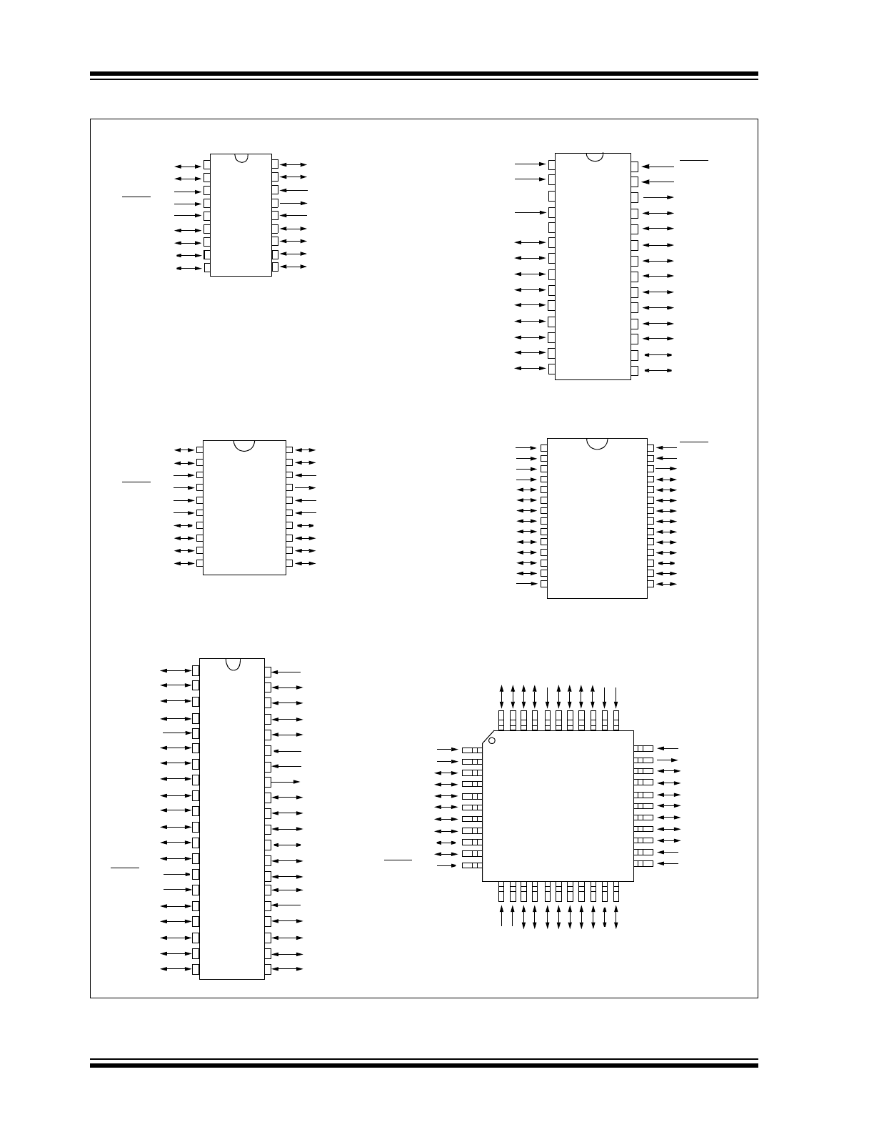
Pin Diagrams
PDIP, SOIC
RA1
RA0
OSC1/CLKIN
OSC2/CLKOUT
V
DD
V
DD
RB7/ICSPDAT
RB6/ICSPCLK
RB5
RB4
RA2
RA3
T0CKI
MCLR/V
PP
V
SS
V
SS
RB0
RB1
RB2
RB3
•
1
2
3
4
5
6
7
8
9
10
20
19
18
17
16
15
14
13
12
11
SSOP
RA2
RA3
T0CKI
MCLR/V
PP
V
SS
RB0
RB1
RB2
RB3
•
1
2
3
4
5
6
7
8
9
10
18
17
16
15
14
13
12
11
RA1
RA0
OSC1/CLKIN
OSC2/CLKOUT
V
DD
RB7/ICSPDAT
RB6/ICSPCLK
RB5
RB4
28
27
26
25
24
23
22
21
20
19
18
17
16
15
•
1
2
3
4
5
6
7
8
9
10
11
12
13
14
PDIP, SOIC
MCLR/V
PP
OSC1/CLKIN
OSC2/CLKOUT
RC7
RC6
RC5
RC4
RC3
RC2
RC1
RC0
RB7/ICSPDAT
RB6/ICSPCLK
RB5
T0CKI
V
DD
V
SS
RA0
RA1
RA2
RA3
RB0
RB1
RB2
RB3
RB4
•
1
2
3
4
5
6
7
8
9
10
11
12
13
14
28
27
26
25
24
23
22
21
20
19
18
17
16
15
SSOP
V
DD
V
SS
T0CKI
V
DD
N/C
V
SS
N/C
RA0
RA1
RA2
RA3
RB0
RB1
RB2
RB3
RB4
MCLR/V
PP
OSC1/CLKIN
OSC2/CLKOUT
RC7
RC6
RC5
RC4
RC3
RC2
RC1
RC0
RB7/ICSPDAT
RB6/ICSPCLK
RB5
PI
C16F
54
PI
C16F
54
PI
C16F
57
PIC16F57
40
39
38
37
36
35
34
33
32
31
30
29
28
27
26
25
24
23
22
21
•
1
2
3
4
5
6
7
8
9
10
11
12
13
14
15
16
17
18
19
20
T0CKI
RE7
RE6
RE5
RE4
V
DD
OSC1/CLKIN
OSC2/CLKOUT
RD7
RD6
RD5
RD4
RD3
RD2
P
IC16F
59
RA0
RA1
RA2
RA3
GND
RB0
RB1
RB2
RB3
RB4
RB5
RB6/ICSPCLK
RB7/ICSPDAT
MCLR/V
PP
V
DD
RC0
RC1
RC2
RC3
RC4
RD1
GND
RD0
RC7
RC6
RC5
PDIP, 0.600"
10
11
2
3
4
5
6
1
18
19
20
21
22
12
13
14
15
38
8
7
44
43
42
41
40
39
16
17
29
30
31
32
33
23
24
25
26
27
28
36
34
35
9
37
RD0
RC7
RC6
RC5
RC4
V
DD
RC3
RC2
RC1
RC0
V
DD
RA
3
RA
2
RA
1
RA
0
RE
7
RE
6
RE
5
RE
4
V
DD
V
DD
OSC1/CLKIN
OSC2/CLKOUT
RD7
RD6
RD5
RD4
RD3
RD2
RD1
GND
GND
GND
GND
RB0
RB1
RB2
RB3
RB4
RB5
RB6/ICSPCLK
RB7/ICSPDAT
MCLR/V
PP
T0
C
K
I
PIC16F59
TQFP

©
2007 Microchip Technology Inc.
DS41213D-page 3
PIC16F5X
Table of Contents
1.0
General Description...................................................................................................................................................................... 5
2.0
Architectural Overview ................................................................................................................................................................. 7
3.0
Memory Organization ................................................................................................................................................................. 13
4.0
Oscillator Configurations ............................................................................................................................................................ 21
5.0
Reset .......................................................................................................................................................................................... 23
6.0
I/O Ports ..................................................................................................................................................................................... 29
7.0
Timer0 Module and TMR0 Register ........................................................................................................................................... 33
8.0
Special Features of the CPU...................................................................................................................................................... 37
9.0
Instruction Set Summary ............................................................................................................................................................ 41
10.0 Development Support................................................................................................................................................................. 53
11.0 Electrical Specifications for PIC16F54/57 .................................................................................................................................. 57
11.0 Electrical Specifications for PIC16F59 (continued) .................................................................................................................... 58
12.0 Packaging Information................................................................................................................................................................ 69
The Microchip Web Site ....................................................................................................................................................................... 83
Customer Change Notification Service ................................................................................................................................................ 83
Customer Support ................................................................................................................................................................................ 83
Reader Response ................................................................................................................................................................................ 84
Product Identification System .............................................................................................................................................................. 85
TO OUR VALUED CUSTOMERS
It is our intention to provide our valued customers with the best documentation possible to ensure successful use of your Microchip
products. To this end, we will continue to improve our publications to better suit your needs. Our publications will be refined and
enhanced as new volumes and updates are introduced.
If you have any questions or comments regarding this publication, please contact the Marketing Communications Department via
E-mail at docerrors@microchip.com or fax the Reader Response Form in the back of this data sheet to (480) 792-4150. We
welcome your feedback.
Most Current Data Sheet
To obtain the most up-to-date version of this data sheet, please register at our Worldwide Web site at:
http://www.microchip.com
You can determine the version of a data sheet by examining its literature number found on the bottom outside corner of any page.
The last character of the literature number is the version number, (e.g., DS30000A is version A of document DS30000).
Errata
An errata sheet, describing minor operational differences from the data sheet and recommended workarounds, may exist for current
devices. As device/documentation issues become known to us, we will publish an errata sheet. The errata will specify the revision
of silicon and revision of document to which it applies.
To determine if an errata sheet exists for a particular device, please check with one of the following:
• Microchip’s Worldwide Web site; http://www.microchip.com
• Your local Microchip sales office (see last page)
When contacting a sales office, please specify which device, revision of silicon and data sheet (include literature number) you are
using.
Customer Notification System
Register on our web site at www.microchip.com to receive the most current information on all of our products.

PIC16F5X
DS41213D-page 4
©
2007 Microchip Technology Inc.
NOTES:
©
2007 Microchip Technology Inc.
DS41213D-page 5
PIC16F5X
1.0
GENERAL DESCRIPTION
The PIC16F5X from Microchip Technology is a family
of low-cost, high-performance, 8-bit, fully static, Flash-
based CMOS microcontrollers. It employs a RISC
architecture with only 33 single-word/single-cycle
instructions. All instructions are single cycle except for
program branches which take two cycles. The
PIC16F5X delivers performance an order of magnitude
higher than its competitors in the same price category.
The 12-bit wide instructions are highly symmetrical
resulting in 2:1 code compression over other 8-bit
microcontrollers in its class. The easy-to-use and easy-
to-remember instruction set reduces development time
significantly.
The PIC16F5X products are equipped with special
features that reduce system cost and power require-
ments. The Power-on Reset (POR) and Device Reset
Timer (DRT) eliminate the need for external Reset
circuitry. There are four oscillator configurations to
choose from, including the power-saving LP (Low
Power) oscillator and cost saving RC oscillator. Power-
saving Sleep mode, Watchdog Timer and code protec-
tion features improve system cost, power and reliability.
The PIC16F5X products are supported by a full-featured
macro assembler, a software simulator, a low-cost devel-
opment programmer and a full featured programmer. All
the tools are supported on IBM
®
PC and compatible
machines.
1.1
Applications
The PIC16F5X series fits perfectly in applications rang-
ing from high-speed automotive and appliance motor
control to low-power remote transmitters/receivers,
pointing devices and telecom processors. The Flash
technology makes customizing application programs
(transmitter codes, motor speeds, receiver
frequencies, etc.) extremely fast and convenient. The
small footprint packages, for through hole or surface
mounting, make this microcontroller series perfect for
applications with space limitations. Low-cost, low-
power, high performance, ease of use and I/O flexibility
make the PIC16F5X series very versatile, even in
areas where no microcontroller use has been
considered before (e.g., timer functions, replacement
of “glue” logic in larger systems, co-processor
applications).
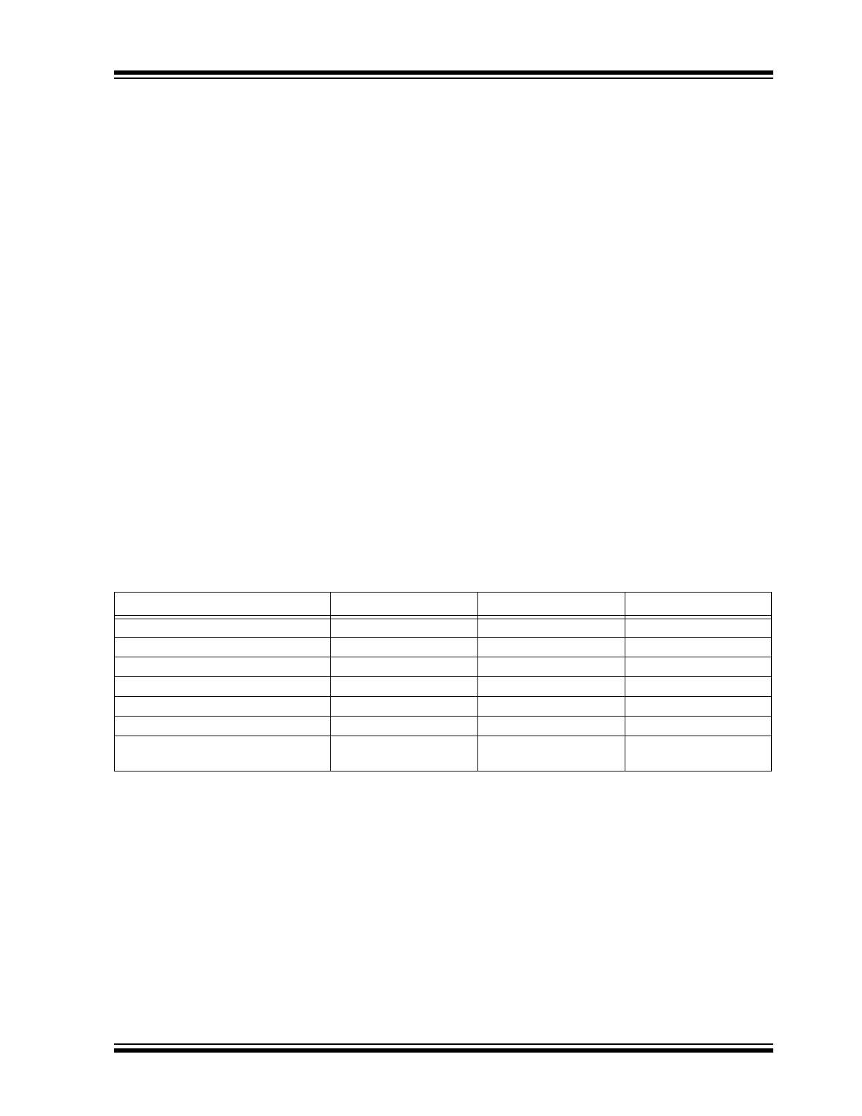
TABLE 1-1:
PIC16F5X FAMILY OF DEVICES
Features
PIC16F54
PIC16F57
PIC16F59
Maximum Operation Frequency
20 MHz
20 MHz
20 MHz
Flash Program Memory (x12 words)
512
2K
2K
RAM Data Memory (bytes)
25
72
134
Timer Module(s)
TMR0
TMR0
TMR0
I/O Pins
12
20
32
Number of Instructions
33
33
33
Packages
18-pin DIP, SOIC;
20-pin SSOP
28-pin DIP, SOIC;
28-pin SSOP
40-pin DIP, 44-pin TQFP
Note:
All PIC
®
Family devices have Power-on Reset, selectable Watchdog Timer, selectable code-protect and
high I/O current capability.

PIC16F5X
DS41213D-page 6
©
2007 Microchip Technology Inc.
NOTES:

©
2007 Microchip Technology Inc.
DS41213D-page 7
PIC16F5X
2.0
ARCHITECTURAL OVERVIEW
The high performance of the PIC16F5X family can be
attributed to a number of architectural features
commonly found in RISC microprocessors. To begin
with, the PIC16F5X uses a Harvard architecture in
which program and data are accessed on separate
buses. This improves bandwidth over traditional von
Neumann architecture where program and data are
fetched on the same bus. Separating program and data
memory further allows instructions to be sized differ-
ently than the 8-bit wide data word. Instruction opcodes
are 12-bits wide, making it possible to have all single-
word instructions. A 12-bit wide program memory
access bus fetches a 12-bit instruction in a single cycle.
A two-stage pipeline overlaps fetch and execution of
instructions. Consequently, all instructions (33) execute
in a single cycle except for program branches.
The PIC16F54 addresses 512 x 12 of program
memory, the PIC16F57 and PIC16F59 addresses
2048 x 12 of program memory. All program memory is
internal.
The PIC16F5X can directly or indirectly address its
register files and data memory. All Special Function
Registers (SFR), including the program counter, are
mapped in the data memory. The PIC16F5X has a
highly orthogonal (symmetrical) instruction set that
makes it possible to carry out any operation on any reg-
ister using any Addressing mode. This symmetrical
nature and lack of ‘special optimal situations’ make pro-
gramming with the PIC16F5X simple, yet efficient. In
addition, the learning curve is reduced significantly.
The PIC16F5X device contains an 8-bit ALU and work-
ing register. The ALU is a general purpose arithmetic
unit. It performs arithmetic and Boolean functions
between data in the working register and any register
file.
The ALU is 8-bits wide and capable of addition,
subtraction, shift and logical operations. Unless other-
wise mentioned, arithmetic operations are two's
complement in nature. In two-operand instructions,
typically one operand is the W (working) register. The
other operand is either a file register or an immediate
constant. In single operand instructions, the operand is
either the W register or a file register.
The W register is an 8-bit working register used for ALU
operations. It is not an addressable register.
Depending on the instruction executed, the ALU may
affect the values of the Carry (C), Digit Carry (DC) and
Zero (Z) bits in the STATUS Register. The C and DC
bits operate as a borrow and digit borrow out bit,
respectively, in subtraction. See the
SUBWF
and
ADDWF
instructions for examples.
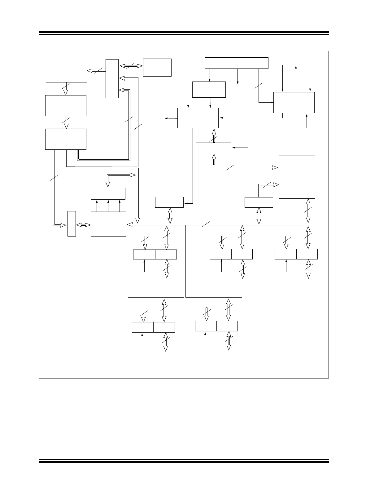
A simplified block diagram is shown in Figure 2-1 with
the corresponding device pins described in Table 2-1
(for PIC16F54), Table 2-2 (for PIC16F57) and
Table 2-3 (for PIC16F59).
PIC16F5X
DS41213D-page 8
©
2007 Microchip Technology Inc.
FIGURE 2-1:
PIC16F5X SERIES BLOCK DIAGRAM
WDT
Time-out
8
Stack 1
Stack 2
Flash
512 X 12 (F54)
2048 X 12(F57)
2048 x 12(F59)
Instruction
Register
Instruction
Decoder
Watchdog
Timer
Configuration Word
Oscillator/
Timing &
Control
General
Purpose
Register
File
(SRAM)
25, 72 or 134
Bytes
WDT/TMR0
Prescaler
Option Reg.
“Option”
“Sleep”
“Code-
Protect”
“Osc
Select”
Direct Address
TMR0
From W
From W
“TRIS 5”
“TRIS 6”
“TRIS 7”
SFR
TRISA
PORTA
TRISB
PORTC
TRISC
PORTB
From W
T0CKI
Pin
9-11
9-11
12
12
8
W
4
4
4
Data Bus
8
8
8
8
8
8
8
ALU
STATUS
From W
CLKOUT
8
9
6
5
5-7
OSC1 OSC2 MCLR
Lit
e
rals
PC
“Disable”
2
RA<3:0>
RB<7:0>
RC<7:0>
PIC16F57/59
only
Direct RAM
Address
“TRIS 8”
PORTD
TRISD
From W
8
8
8
RD<7:0>
PIC16F59
only
“TRIS 9”
PORTE
TRISE
From W
4
4
RE<7:4>
PIC16F59
only
8