
1999-2013 Microchip Technology Inc.
DS41106C-page 1
PIC16C712/716
Devices included in this Data Sheet:
• PIC16C712
• PIC16C716
Microcontroller Core Features:
• High-performance RISC CPU
• Only 35 single-word instructions to learn
• All single-cycle instructions except for program
branches which are two cycle
• Operating speed: DC – 20 MHz clock input
DC – 200 ns instruction cycle
• Interrupt capability
(up to 7 internal/external interrupt sources)
• Eight-level deep hardware stack
• Direct, Indirect and Relative Addressing modes
• Power-on Reset (POR)
• Power-up Timer (PWRT) and
Oscillator Start-up Timer (OST)
• Watchdog Timer (WDT) with its own on-chip RC
oscillator for reliable operation
• Brown-out detection circuitry for
Brown-out Reset (BOR)
• Programmable code-protection
• Power-saving Sleep mode
• Selectable oscillator options
• Low-power, high-speed CMOS EPROM
technology
• Fully static design
• In-Circuit Serial Programming
(ICSP™)
• Wide operating voltage range: 2.5V to 5.5V
• High Sink/Source Current 25/25 mA
• Commercial, Industrial and Extended temperature
ranges
• Low-power consumption:
- < 2 mA @ 5V, 4 MHz
- 22.5
A, typical @ 3V, 32 kHz
- < 1
A, typical standby current
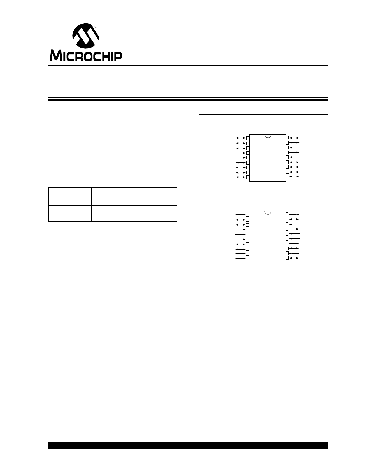
Pin Diagrams
Peripheral Features:
• Timer0: 8-bit timer/counter with 8-bit prescaler
• Timer1: 16-bit timer/counter with prescaler
can be incremented during Sleep via external
crystal/clock
• Timer2: 8-bit timer/counter with 8-bit period
register, prescaler and postscaler
• Capture, Compare, PWM module
• Capture is 16-bit, max. resolution is 12.5 ns,
Compare is 16-bit, max. resolution is 200 ns,
PWM maximum resolution is 10-bit
• 8-bit multi-channel Analog-to-Digital converter
Device
Program
Memory
Data Memory
PIC16C712
1K
128
PIC16C716
2K
128
PI
C16C712
RA2/AN2
RA4/T0CKI
RB0/INT
RB1/T1OSO/T1CKI
RA0/AN0
OSC1/CLKIN
RB7
RB6
1
2
3
4
5
6
7
18
17
16
15
14
13
12
8
9
11
10
18-pin PDIP, SOIC, Windowed CERDIP
MCLR/V
PP
RA3/AN3/V
REF
RB2/T1OSI
RB3/CCP1
RB4
RB5
RA1/AN1
V
DD
OSC2/CLKOUT
V
SS
PI
C16C716
P
IC16C
712
RA2/AN2
RA4/T0CKI
RB0/INT
RB1/T1OSO/T1CKI
RA0/AN0
OSC1/CLKIN
RB7
RB6
1
2
3
4
5
6
7
20
19
18
17
16
15
14
8
9
13
12
20-pin SSOP
MCLR/V
PP
RA3/AN3/V
REF
RB2/T1OSI
RB3/CCP1
RB4
RB5
RA1/AN1
V
DD
OSC2/CLKOUT
V
SS
P
IC16C
716
10
V
SS
V
DD
11
8-Bit CMOS Microcontrollers with A/D Converter
and Capture/Compare/PWM
PIC16C712/716
DS41106C-page 2
1999-2013 Microchip Technology Inc.
PIC16C7XX FAMILY OF DEVICES
Key Features
PIC
®
Mid-Range Reference Manual (DS33023)
PIC16C712
PIC16C716
Operating Frequency
DC – 20 MHz
DC – 20 MHz
Resets (and Delays)
POR, BOR (PWRT, OST)
POR, BOR (PWRT, OST)
Program Memory (14-bit words)
1K
2K
Data Memory (bytes)
128
128
Interrupts
7
7
I/O Ports
Ports A,B
Ports A,B
Timers
3
3
Capture/Compare/PWM modules
1
1
8-bit Analog-to-Digital Module
4 input channels
4 input channels
PIC16C710
PIC16C71
PIC16C711
PIC16C712
PIC16C715
PIC16C716
PIC16C72A PIC16C73B
Clock
Maximum Frequency
of Operation (MHz)
20
20
20
20
20
20
20
20
Memory
EPROM Program
Memory
(x14 words)
512
1K
1K
1K
2K
2K
2K
4K
Data Memory (bytes)
36
36
68
128
128
128
128
192
Peripherals
Timer Module(s)
TMR0
TMR0
TMR0
TMR0
TMR1
TMR2
TMR0
TMR0
TMR1
TMR2
TMR0
TMR1
TMR2
TMR0
TMR1
TMR2
Capture/Compare/
PWM Module(s)
—
—
—
1
—
1
1
2
Serial Port(s)
(SPI™/I
2
C™, USART)
—
—
—
—
—
—
SPI/I
2
C
SPI/I
2
C,
USART
A/D Converter (8-bit)
Channels
4
4
4
4
4
4
5
5
Features
Interrupt Sources
4
4
4
7
4
7
8
11
I/O Pins
13
13
13
13
13
13
22
22
Voltage Range (Volts)
2.5-6.0
3.0-6.0
2.5-6.0
2.5-5.5
2.5-5.5
2.5-5.5
2.5-5.5
2.5-5.5
In-Circuit Serial
Programming™
Yes
Yes
Yes
Yes
Yes
Yes
Yes
Yes
Brown-out Reset
Yes
—
Yes
Yes
Yes
Yes
Yes
Yes
Packages
18-pin DIP,
SOIC;
20-pin SSOP
18-pin DIP,
SOIC
18-pin DIP,
SOIC;
20-pin SSOP
18-pin DIP,
SOIC;
20-pin SSOP
18-pin DIP,
SOIC;
20-pin SSOP
18-pin DIP,
SOIC;
20-pin SSOP
28-pin SDIP,
SOIC, SSOP
28-pin SDIP,
SOIC

1999-2013 Microchip Technology Inc.
DS41106C-page 3
PIC16C712/716
Table of Contents
1.0
Device Overview .......................................................................................................................................................................... 5
2.0
Memory Organization ................................................................................................................................................................... 9
3.0
I/O Ports ..................................................................................................................................................................................... 21
4.0
Timer0 Module ........................................................................................................................................................................... 29
5.0
Timer1 Module ........................................................................................................................................................................... 31
6.0
Timer2 Module ........................................................................................................................................................................... 36
7.0
Capture/Compare/PWM (CCP) Module(s) ................................................................................................................................. 39
8.0
Analog-to-Digital Converter (A/D) Module .................................................................................................................................. 45
9.0
Special Features of the CPU...................................................................................................................................................... 51
10.0 Instruction Set Summary ............................................................................................................................................................ 67
11.0 Development Support................................................................................................................................................................. 69
12.0 Electrical Characteristics ............................................................................................................................................................ 73
13.0 Packaging Information................................................................................................................................................................ 89
Revision History .................................................................................................................................................................................. 95
Conversion Considerations ................................................................................................................................................................. 95
Migration from Base-line to Mid-Range Devices ................................................................................................................................. 95
Index ................................................................................................................................................................................................... 97
On-Line Support................................................................................................................................................................................. 101
Reader Response .............................................................................................................................................................................. 102
PIC16C712/716 Product Identification System .................................................................................................................................. 103
TO OUR VALUED CUSTOMERS
It is our intention to provide our valued customers with the best documentation possible to ensure successful use of your Microchip
products. To this end, we will continue to improve our publications to better suit your needs. Our publications will be refined and
enhanced as new volumes and updates are introduced.
If you have any questions or comments regarding this publication, please contact the Marketing Communications Department via
E-mail at docerrors@microchip.com or fax the Reader Response Form in the back of this data sheet to (480) 792-4150. We
welcome your feedback.
Most Current Data Sheet
To obtain the most up-to-date version of this data sheet, please register at our Worldwide Web site at:
http://www.microchip.com
You can determine the version of a data sheet by examining its literature number found on the bottom outside corner of any page.
The last character of the literature number is the version number, (e.g., DS30000A is version A of document DS30000).
Errata
An errata sheet, describing minor operational differences from the data sheet and recommended workarounds, may exist for current
devices. As device/documentation issues become known to us, we will publish an errata sheet. The errata will specify the revision
of silicon and revision of document to which it applies.
To determine if an errata sheet exists for a particular device, please check with one of the following:
• Microchip’s Worldwide Web site; http://www.microchip.com
• Your local Microchip sales office (see last page)
When contacting a sales office, please specify which device, revision of silicon and data sheet (include literature number) you are
using.
Customer Notification System
Register on our web site at www.microchip.com to receive the most current information on all of our products.

PIC16C712/716
DS41106C-page 4
1999-2013 Microchip Technology Inc.
NOTES:
1999-2013 Microchip Technology Inc.
DS41106C-page 5
PIC16C712/716
1.0
DEVICE OVERVIEW
This document contains device-specific information.
Additional information may be found in the PIC
®
Mid-
Range Reference Manual, (DS33023), which may be
obtained from your local Microchip Sales Representa-
tive or downloaded from the Microchip web site. The
Reference Manual should be considered a comple-
mentary document to this data sheet, and is highly rec-
ommended reading for a better understanding of the
device architecture and operation of the peripheral
modules.
There are two devices (PIC16C712, PIC16C716)
covered by this data sheet.
Figure 1-1 is the block diagram for both devices. The
pinouts are listed in Table 1-1.
FIGURE 1-1:
PIC16C712/716 BLOCK DIAGRAM
EPROM
Program
Memory
13
Data Bus
8
14
Program
Bus
Instruction Reg
Program Counter
8 Level Stack
(13-bit)
RAM
File
Registers
Direct Addr
7
RAM Addr
(1)
9
Addr MUX
Indirect
Addr
FSR Reg
STATUS Reg
MUX
ALU
W Reg
Power-up
Timer
Oscillator
Start-up Timer
Power-on
Reset
Watchdog
Timer
Instruction
Decode &
Control
Timing
Generation
OSC1/CLKIN
OSC2/CLKOUT
MCLR
V
DD
, V
SS
PORTA
PORTB
RB0/INT
RB1/T1OSO/T1CKI
RB2/T1OSI
RB3/CCP1
RB4
RB5
RB6
RB7
8
8
Brown-out
Reset
Note 1: Higher order bits are from the STATUS register.
CCP1
A/D
Timer0
Timer1
Timer2
RA4/T0CKI
RA3/AN3/V
REF
RA2/AN2
RA1/AN1
RA0/AN0
8
3
1K X 14
128 x 8
or
2K x 14
PIC16C712/716
DS41106C-page 6
1999-2013 Microchip Technology Inc.
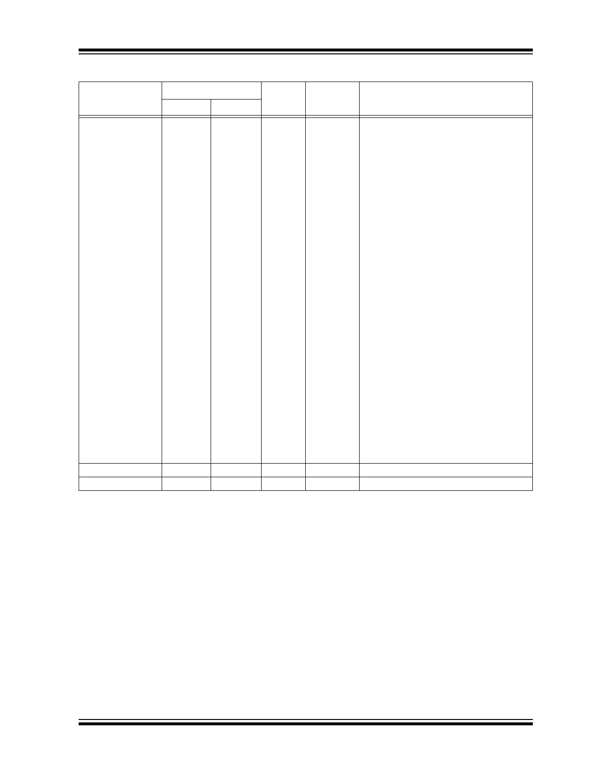
TABLE 1-1:
PIC16C712/716 PINOUT DESCRIPTION
Pin
PIC16C712/716
Pin
Buffer
Name
DIP, SOIC
SSOP
Type
Type
Description
MCLR/V
PP
MCLR
V
PP
4
4
I
P
ST
Master clear (Reset) input. This pin is
an active low Reset to the device.
Programming voltage input
OSC1/CLKIN
OSC1
CLKIN
16
18
I
I
ST
CMOS
Oscillator crystal input or external clock
source input. ST buffer when config-
ured in RC mode. CMOS otherwise.
External clock source input.
OSC2/CLKOUT
OSC2
CLKOUT
15
17
O
O
—
—
Oscillator crystal output. Connects to
crystal or resonator in crystal oscillator
mode.
In RC mode, OSC2 pin outputs
CLKOUT which has 1/4 the frequency
of OSC1, and denotes the instruction
cycle rate.
PORTA is a bidirectional I/O port.
RA0/AN0
RA0
AN0
17
19
I/O
I
TTL
Analog
Digital I/O
Analog input 0
RA1/AN1
RA1
AN1
18
20
I/O
I
TTL
Analog
Digital I/O
Analog input 1
RA2/AN2
RA2
AN2
1
1
I/O
I
TTL
Analog
Digital I/O
Analog input 2
RA3/AN3/V
REF
RA3
AN3
V
REF
2
2
I/O
I
I
TTL
Analog
Analog
Digital I/O
Analog input 3
A/D Reference Voltage input.
RA4/T0CKI
RA4
T0CKI
3
3
I/O
I
ST/OD
ST
Digital I/O. Open drain when configured
as output.
Timer0 external clock input
Legend: TTL = TTL-compatible input
CMOS = CMOS compatible input or output
ST = Schmitt Trigger input with CMOS levels
OD = Open drain output
SM = SMBus compatible input. An external resistor is required if this pin is used as an output
NPU = N-channel pull-up
PU = Weak internal pull-up
No-P diode = No P-diode to V
DD
AN = Analog input or output
I = input
O = output
P = Power
L = LCD Driver
1999-2013 Microchip Technology Inc.
DS41106C-page 7
PIC16C712/716
PORTB is a bidirectional I/O port. PORTB
can be software programmed for internal
weak pull-ups on all inputs.
RB0/INT
RB0
INT
6
7
I/O
I
TTL
ST
Digital I/O
External Interrupt
RB1/T1OSO/T1CKI
RB1
T1OSO
T1CKI
7
8
I/O
O
I
TTL
—
ST
Digital I/O
Timer1 oscillator output. Connects to
crystal in oscillator mode.
Timer1 external clock input.
RB2/T1OSI
RB2
T1OSI
8
9
I/O
I
TTL
—
Digital I/O
Timer1 oscillator input. Connects to
crystal in oscillator mode.
RB3/CCP1
RB3
CCP1
9
10
I/O
I/O
TTL
ST
Digital I/O
Capture1 input, Compare1 output,
PWM1 output.
RB4
10
12
I/O
TTL
Digital I/O
Interrupt on change pin.
RB5
11
12
I/O
TTL
Digital I/O
Interrupt on change pin.
RB6
12
13
I/O
I
TTL
ST
Digital I/O
Interrupt on change pin.
ICSP programming clock.
RB7
13
14
I/O
I/O
TTL
ST
Digital I/O
Interrupt on change pin.
ICSP programming data.
V
SS
5
5, 6
P
—
Ground reference for logic and I/O pins.
V
DD
14
15, 16
P
—
Positive supply for logic and I/O pins.
Legend: TTL = TTL-compatible input
CMOS = CMOS compatible input or output
ST = Schmitt Trigger input with CMOS levels
OD = Open drain output
SM = SMBus compatible input. An external resistor is required if this pin is used as an output
NPU = N-channel pull-up
PU = Weak internal pull-up
No-P diode = No P-diode to V
DD
AN = Analog input or output
I = input
O = output
P = Power
L = LCD Driver
TABLE 1-1:
PIC16C712/716 PINOUT DESCRIPTION (CONTINUED)
Pin
PIC16C712/716
Pin
Buffer
Name
DIP, SOIC
SSOP
Type
Type
Description

PIC16C712/716
DS41106C-page 8
1999-2013 Microchip Technology Inc.
NOTES:
1999-2013 Microchip Technology Inc.
DS41106C-page 9
PIC16C712/716
2.0
MEMORY ORGANIZATION
There are two memory blocks in each of these PIC
®
microcontroller devices. Each block (Program Memory
and Data Memory) has its own bus so that concurrent
access can occur.
Additional information on device memory may be found
in the PIC
®
Mid-Range Reference Manual, (DS33023).
2.1
Program Memory Organization
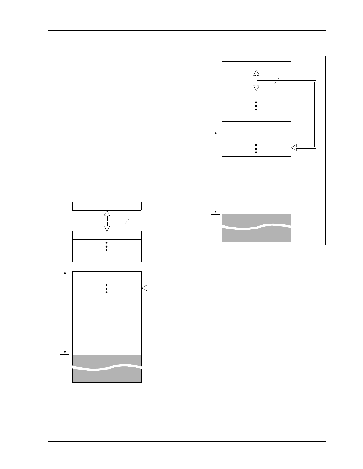
The PIC16C712/716 has a 13-bit Program Counter
(PC) capable of addressing an 8K x 14 program mem-
ory space. PIC16C712 has 1K x 14 words of program
memory and PIC16C716 has 2K x 14 words of program
memory. Accessing a location above the physically
implemented address will cause a wraparound.
The Reset vector is at 0000h and the interrupt vector is
at 0004h.
FIGURE 2-1:
PROGRAM MEMORY MAP
AND STACK OF THE
PIC16C712
FIGURE 2-2:
PROGRAM MEMORY MAP
AND STACK OF PIC16C716
PC<12:0>
13
0000h
0004h
0005h
03FFh
1FFFh
Stack Level 1
Stack Level 8
Reset Vector
Interrupt Vector
On-chip Program
Memory
CALL, RETURN
RETFIE, RETLW
0400h
Use
r Me
mo
ry
S
pac
e
PC<12:0>
13
0000h
0004h
0005h
07FFh
0800h
1FFFh
Stack Level 1
Stack Level 8
Reset Vector
Interrupt Vector
On-chip Program
Memory
CALL, RETURN
RETFIE, RETLW
U
s
er
Me
mo
ry
Sp
a
c
e
PIC16C712/716
DS41106C-page 10
1999-2013 Microchip Technology Inc.
2.2
Data Memory Organization
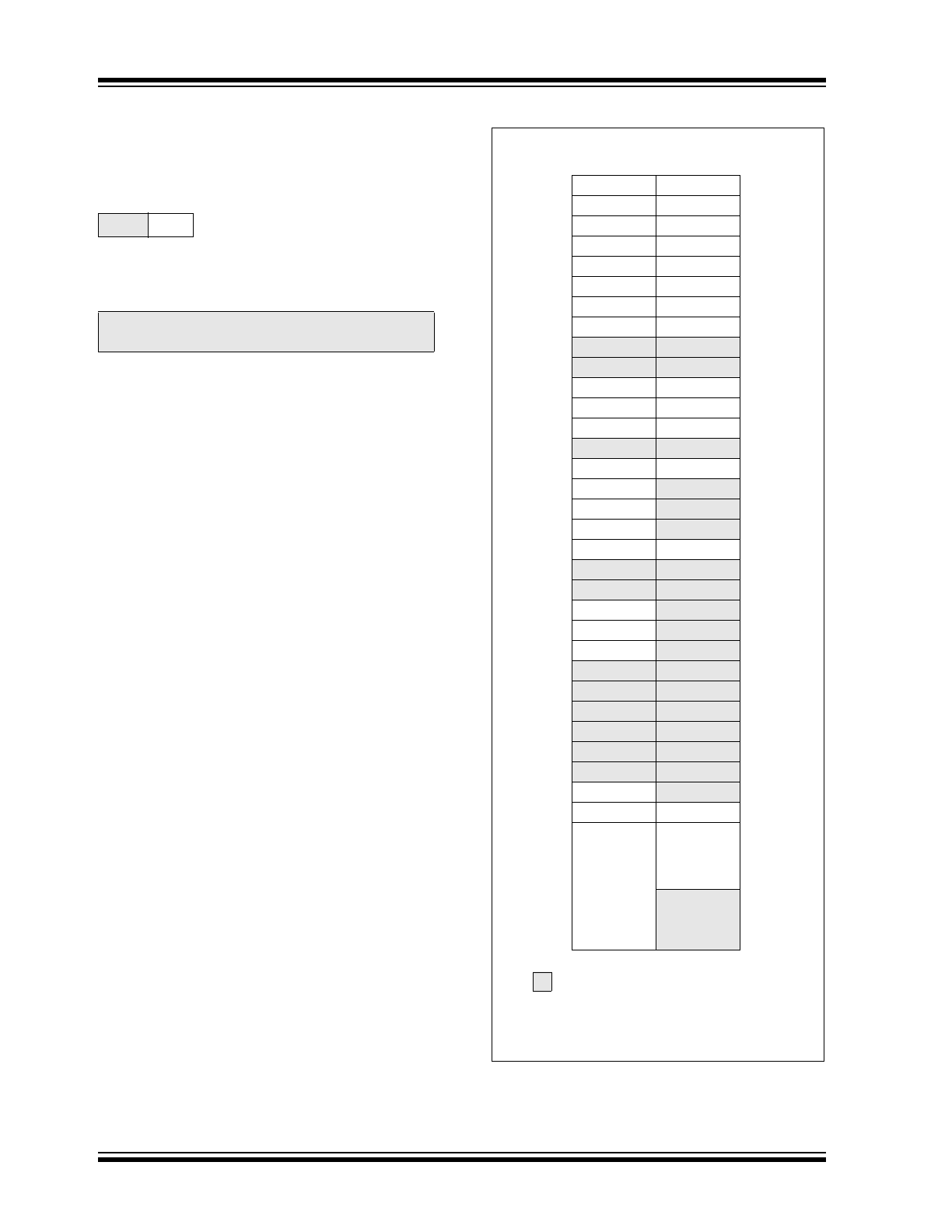
The data memory is partitioned into multiple banks
which contain the General Purpose Registers and the
Special Function Registers. Bits RP1 and RP0 are the
bank select bits.
= 00
Bank 0
= 01
Bank 1
= 10
Bank 2 (not implemented)
= 11
Bank 3 (not implemented)
Each bank extends up to 7Fh (128 bytes). The lower
locations of each bank are reserved for the Special
Function Registers. Above the Special Function Regis-
ters are General Purpose Registers, implemented as
static RAM. All implemented banks contain Special
Function Registers. Some “high use” Special Function
Registers from one bank may be mirrored in another
bank for code reduction and quicker access.
2.2.1
GENERAL PURPOSE REGISTER
FILE
The register file can be accessed either directly, or
indirectly through the File Select Register FSR (see
Section 2.5 “Indirect Addressing, INDF and FSR
Registers”).
FIGURE 2-3:
REGISTER FILE MAP
RP1
(1)
RP0
(STATUS<6:5>)
Note 1:
Maintain this bit clear to ensure upward
compatibility with future products.
Unimplemented data memory locations,
read as ‘0’.
Note 1: Not a physical register.
File
Address
File
Address
00h
INDF
(1)
INDF
(1)
80h
01h
TMR0
OPTION_REG
81h
02h
PCL
PCL
82h
03h
STATUS
STATUS
83h
04h
FSR
FSR
84h
05h
PORTA
TRISA
85h
06h
PORTB
TRISB
86h
07h
DATACCP
TRISCCP
87h
08h
88h
09h
89h
0Ah
PCLATH
PCLATH
8Ah
0Bh
INTCON
INTCON
8Bh
0Ch
PIR1
PIE1
8Ch
0Dh
8Dh
0Eh
TMR1L
PCON
8Eh
0Fh
TMR1H
8Fh
10h
T1CON
90h
11h
TMR2
91h
12h
T2CON
PR2
92h
13h
93h
14h
94h
15h
CCPR1L
95h
16h
CCPR1H
96h
17h
CCP1CON
97h
18h
98h
19h
99h
1Ah
9Ah
1Bh
9Bh
1Ch
9Ch
1Dh
9Dh
1Eh
ADRES
9Eh
1Fh
ADCON0
ADCON1
9Fh
20h
General
Purpose
Registers
96 Bytes
General
Purpose
Registers
32 Bytes
A0h
BFh
C0h
7Fh
FFh
Bank 0
Bank 1