

Atmel ATFEE560
Multi-Chip Rad-Hard Modules:
Reprogrammable FPGA matrix (ATF280) (x2)
EEPROM Memory (AT69170) (x2)
DATASHEET
Features
Non Volatile Rad Hard Reprogrammable FPGA
ATF280 SRAM-based FPGA
AT69170 Serial EEPROM
2x SRAM-based FPGA designed for Space use - ATF280
560K equivalent ASIC gates
28,800 cells ( two 3-input LUT or one 4-input LUT, one DFF)
Unlimited reprogrammability
SEE-hardened (Configuration RAM, DPRAM, DFF, I/O buffers)
Rad Hard by Design - No need for mitigation techniques during design
Available DPRAM ressources in the ATF280
230,400 bits of distributed RAM
Organized in 32x4 blocks of DPRAM
Independent of Logic Cells
Single/Dual port capability
Reset System
Individual reset on each FPGA
Possibility to reset simultaneously both FPGAs
Clock System
2 global clocks shared between both FPGAs
6 global clocks and 2 fast clocks on FPGA 1
6 global clocks and 2 fast clocks on FPGA 2
Flexible serial configuration
Integrated 4Mbits serial non volatile memory
On chip redundant configuration memory
Designed to store Field Programmable Gate Arrays Configurations
In-System Programming (ISP) via Two-Wire Interface
Master/Slave configuration capability
Configuration Integrity Check
Check of the data during FPGA application download
Self Integrity Check (CSIC) of the configuration during FPGA operation
User IOs
Cold-sparing and PCI-compliant I/Os:
24 General Purpose IOs internally shared by both FPAGs and externally
accessible
131 General Purpose IOs internally shared by both FPAGs
107 General Purpose IOs only for FPGA1
41041B
AERO
09/15

ATFEE560 [DATASHEET]
41041B
AERO
09/15
2
146 General Purpose IOs only for FPGA2
4 LVDS transmitters on FPGA2
4 LVDS receivers on FPGA2
Performance
50MHz system performance
10ns 32X4 DPRAM access time
Operating range
Voltages
1.65V to 1.95V (Core)
3V to 3.6V (Clustered I/Os)
Temperature
- 55°C to +125°C
Radiation performance
Total dose tested up to 60 krads (Si)
AT69170, TID tested up to 60 krads (unbiased)
ATF280, TID tested up to 300 krads
No single event latch-up below a LET of 95 MeV/mg/cm2
ESD better than 2000V for I/O and better than 1000V for LVDS
Quality grades
QML-Q or V
Description
The ATFEE560 is a radiation-hardened reprogrammable FPGA, especially designed for
space applications. For low-power consumption applications, the ATFEE560 is a new
device offering many advantages.
The ATFEE560 relies on Atmel ATF280 space qualified SRAM based FPGA together with
the Atmel AT69170 serial configuration EEPROM memory.
The ATFEE560 features an innovative built-in SEU protection, which eliminates the need
for Triple-Module-Redundancy (TMR). Its re-programmability makes multiple design
iterations possible. Moreover, post-programming burn-in is not necessary.
With the integration of redundant serial programming eeproms inside the package, the
ATFEE560 is perfectly suited for application requiring small footprint.
The Development Kit lets to evaluate the ATFEE560 quickly and economically, running
simple demonstrations as well as your complete applications. Throughout your
development, from concept to final integration, Atmel provides the tools and support to
help you successfully integrate your application into the ATFEE560.
The ATFEE560 is available in MQFP352 package and features 277 standard I/Os and 8
LVDS I/Os (4 Rx and 4Tx) for the user application.
Table 1.
ATFEE560 Summary
Function
ATFEE560
Available ASIC Gates (50% typ. routable)
2x 280K / 560K
RAM Bits
2x 115 200 / 230 400
Core Cells
2x 14 400 / 28 800
I/O
277
LVDS (Rx/Tx)
4 Rx / 4 Tx
ATFEE560 [DATASHEET]
41041B
AERO
09/15
3
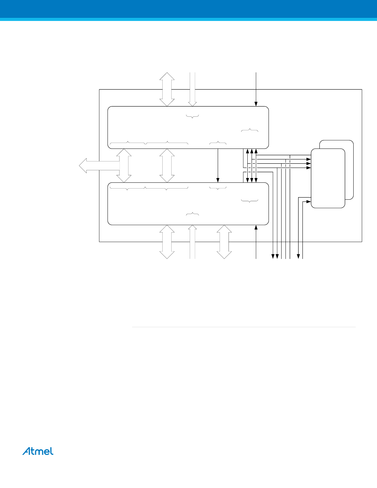
Figure 2.
ATFEE560 Overview
DATA
CLK
/CE
/RESET_OE
READY
SER_EN
Internally shared
IO[130:0]
IO_FPGA2
[144:0]
FPGA2
ILVDS[3:0]
ILVDSn[3:0]
OLVDS[3:0]
OLVDSn[3:0]
IO_FPGA1
[105:0]
Serial Cfg Interface
IN
IT
C
O
N
C
C
L
K
D
0
IN
IT
C
O
N
C
C
L
K
D
0
Serial Cfg Interface
CSOUT
CS0
Cascading
Interface
M
2
M
1
M
0
Mode
RESETN
FPGA_1
FPGA_2
NVM_1
NVM_2
M
2
M
1
M
0
Mode
RESETN
Mode
FPGA1
Mode
FPGA2
Reset
FPGA1
Reset
FPGA2
Cascading
Interface
IN
IT
_
F
1
C
O
N
C
C
L
K
D
0
R
E
A
D
Y
S
E
R
_
E
N
Internally shared
IO[130:0]
Internally shared
IO[23:0]
External access of
shared IO[23:0]
Internally shared
IO[23:0]
IN
IT
_
F
2
References
ATF280 Datasheet
– ref : doc7750
AT69170 Datasheet
– ref : doc41069

ATFEE560 [DATASHEET]
41041B
AERO
09/15
4
Table of Contents
1.
Glossary ............................................................................................. 5
2.
Dies connections ................................................................................ 6
2.1
PINOUT ............................................................................................................ 6
2.1.1
FPGA1 ............................................................................................. 6
2.1.1.1
General Purpose IOs ........................................................ 6
2.1.1.2
Supply ............................................................................... 7
2.1.1.3
Configuration IOs .............................................................. 7
2.1.2
FPGA2 ............................................................................................. 8
2.1.2.1
General Purpose IOs ........................................................ 8
2.1.2.2
LVDS ............................................................................... 9
2.1.2.3
Supply ............................................................................. 10
2.1.2.4
Configuration IOs ............................................................ 10
2.1.3
Pins shared by both FPGAs .............................................................. 10
2.1.3.1
General Purpose Ios ....................................................... 10
2.1.3.2
Configuration IOs ............................................................ 11
2.1.4
NVM_1 and NVM_2 .......................................................................... 12
2.1.4.1
Configuration IOs ............................................................ 12
2.1.4.2
Supply ............................................................................. 12
2.1.5
Pins shared by both memories and both FPGA ................................ 12
2.1.6
JTAG ........................................................................................... 13
2.2
IOs from both FPGAs connected internally ..................................................... 13
3.
Configuration Download ................................................................... 15
3.1
Master serial mode
– Mode 0 .......................................................................... 15
3.2
Slave serial mode
– mode 1 ............................................................................ 16
3.3
Available ATFEE560 configurations ................................................................ 16
3.3.1
FPGA1 master
– FPGA2 slave ......................................................... 16
3.3.2
FPGA1 slave
– FPGA2 slave ............................................................ 19
4.
Ordering Information ........................................................................ 20
4.1
ATFEE560FF Ordering Codes ........................................................................ 20
4.2
ATFEE560 Evaluation Kit Ordering Codes ..................................................... 20
5.
Revision History ............................................................................... 21

ATFEE560 [DATASHEET]
41041B
AERO
09/15
5
1.
Glossary
FPGA
Field Programmable Gate Array
POR
Power On Reset
SRAM
Static Random Access Memory
SEU
Single Event Upset
CSIC
Configuration Self Internal Checker
TWI
Two wire Interface
ATFEE560 [DATASHEET]
41041B
AERO
09/15
6
2.
Dies connections
The aim here is to describe all the IO connections for each die implemented in the ATFEE560 ( 2x ATF280 and 2x
AT69170). The serial programmation mode has been privileged due to the limited number of pakages pins.
Both FPGA have three connection types for their General Purpose IOs, here after their descriptions and their number:
24 General Purpose IOs internally shared by both FPAGs and externally accessible
131 General Purpose IOs internally shared by both FPAGs
107 General Purpose IOs dedicated to FPGA1 and 146 General Purpose IOs dedicated to FPGA2 (including
INIT signals)
Each FPGA and each non-volatile memory has a dedicated supply.
2.1
PINOUT
2.1.1
FPGA1
2.1.1.1
General Purpose IOs
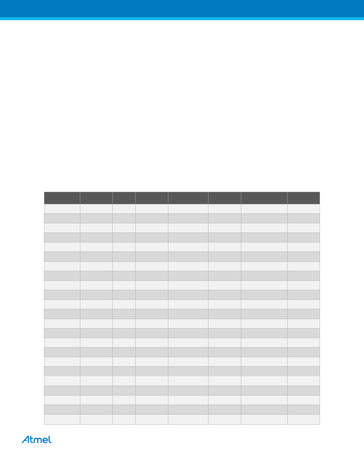
Table 2-1.
FPGA1, General Purpose IOs
IO
MQFP352
IO
MQFP352
IO
MQFP352
IO
MQFP352
IO1_GCK1
10
IO79
39
IO173
70
IO259_LDC (*)
103
IO5
11
IO83
40
IO175
71
IO263
104
IO7
12
IO85
41
IO177
72
IO265_HDC (*)
105
IO11
13
IO87
42
IO180_FCK2
73
IO267
106
IO13
14
IO93
43
IO185
74
IO273
108
IO17
15
IO97
44
IO187
75
IO277
109
IO19
16
IO99
47
IO191
76
IO279
110
IO23
17
IO103
48
IO193
77
IO283
113
IO25
18
IO105
49
IO197
78
IO480_GCK4
114
IO27
19
IO111
50
IO199
79
IO722_GCK7
116
IO31
20
IO125
51
IO203
80
IO917
135
IO33
21
IO127
52
IO205
81
IO919
136
IO37
22
IO131
53
IO207
82
IO923
137
IO39
25
IO133
54
IO213
83
IO925
138
IO43
26
IO137
55
IO217
84
IO927
139
IO45
27
IO139
56
IO219
85
IO931
140
IO47
28
IO143
57
IO223
86
IO937
141
IO51
29
IO145
58
IO227
92
IO939
142
IO53
30
IO147
59
IO231
93
IO943
143
IO57
31
IO151
60
IO233
94
IO945
144
IO61_FCK1
32
IO153
61
IO237
95
IO947
145
IO63
33
IO157
62
IO240_GCK2
96
IO951
146
IO65
34
IO159
63
IO245
98
IO953
147
ATFEE560 [DATASHEET]
41041B
AERO
09/15
7
IO67
35
IO163
64
IO247
99
IO960
149
IO71
36
IO165
65
IO251
100
IO303_INIT (*)
150
IO73
37
IO167
66
IO253
101
IO547_CS0 (*)
267
IO77
38
IO171
69
IO257
102
(*) : this general purpose IO is a configuration IO during configuration download
2.1.1.2
Supply
Table 2-2.
FPGA1, supply
GROUND
MQFP352
VDD = 1,8V
MQFP352
VCC = 3,3V
MQFP352
GND
1
VDD
2
VCC
24
GND
23
VDD
46
VCC
68
GND
45
VDD
88
VCC
112
GND
67
VDD
90
GND
87
VDD
134
GND
89
VDD
352
GND
111
GND
133
GND
156
2.1.1.3
Configuration IOs
Table 2-3.
FPGA1, configuration IOs
Configuration IO name
MQFP352
M0
7
M1
8
M2
9
IO259_LDC
103
IO265_HDC
105
IO303_INIT
150
IO547_CS0
267
RESETN
342
ATFEE560 [DATASHEET]
41041B
AERO
09/15
8
2.1.2
FPGA2
2.1.2.1
General Purpose IOs
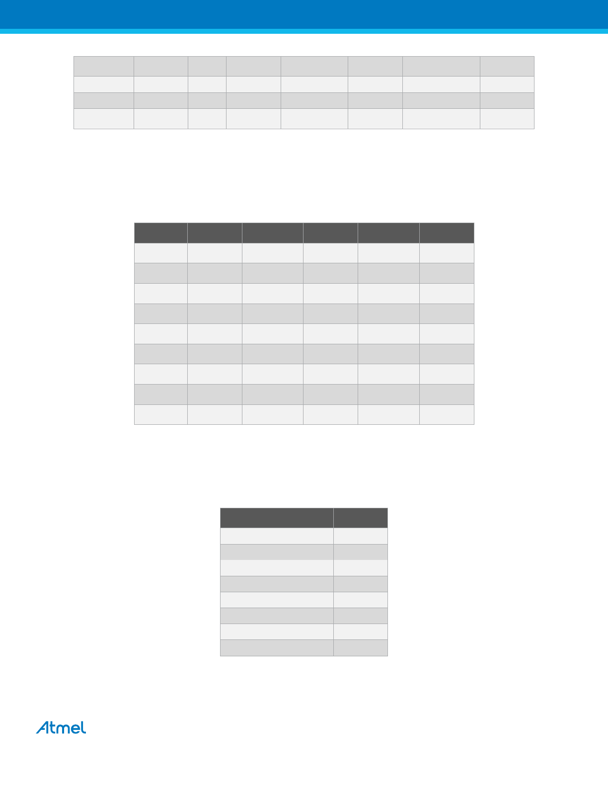
Table 2-4.
FPGA2, General purpose IOs
IO
MQFP352
IO
MQFP352
IO
MQFP352
IO
MQFP352
IO1_GCK1
153
IO507
205
IO625
256
IO757
300
IO399
163
IO511
206
IO639
257
IO759
301
IO403
164
IO513
207
IO643
258
IO763
302
IO405
165
IO517
208
IO645
259
IO765
303
IO407
166
IO519
209
IO647
260
IO767
304
IO411
167
IO523
210
IO651
261
IO771
305
IO413
168
IO525
211
IO653
262
IO773
306
IO417
169
IO527
212
IO658_FCK4
268
IO777
307
IO419
170
IO531
213
IO661
269
IO779
308
IO423
171
IO533
214
IO665
270
IO783
311
IO425
172
IO537
215
IO667
271
IO785
312
IO427
173
IO539
216
IO671
272
IO787
313
IO303_INIT
(*)
174
IO543_FCK3
217
IO673
273
IO791
314
IO433
179
IO545
218
IO677
274
IO793
315
IO437
180
IO551
220
IO679
275
IO797
316
IO439
181
IO553
223
IO683
276
IO799
317
IO443
182
IO557
224
IO685
277
IO803
318
IO445
183
IO559
225
IO687
278
IO805
319
IO447
184
IO563
226
IO691
279
IO807
320
IO453
185
IO565
227
IO693
280
IO811
321
IO457
186
IO567
228
IO697
281
IO813
322
IO459
187
IO571
229
IO699
282
IO817
323
IO463
188
IO573
230
IO703
283
IO819
324
IO465
189
IO577
231
IO705
284
IO823
325
IO467
190
IO579
232
IO707
285
IO825
326
IO471
191
IO583
233
IO711
286
IO831
327
IO473
192
IO585
234
IO717
289
IO833
328
IO477
193
IO591
235
IO720_GCK6_CSOUTN
(*)
290
IO847
329
IO480_GCK4
194
IO605
244
IO722_GCK7
291
IO851
330
IO482_GCK5
195
IO607
245
IO725
292
IO853
333
IO485
196
IO611
246
IO733
293
IO857
334
IO487
197
IO613
249
IO737
294
IO859
335
ATFEE560 [DATASHEET]
41041B
AERO
09/15
9
IO491
198
IO617
250
IO739
295
IO863
336
IO493
201
IO619
251
IO745
296
IO865
337
IO497
202
IO623
252
IO747
297
IO960_GCK8_
338
IO503
203
IO627
254
IO751
298
IO505
204
IO633
255
IO753
299
(*) : this general purpose IO is also a configuration IO during configuration download
2.1.2.2
LVDS
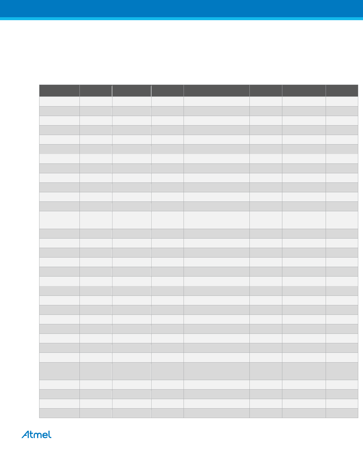
Table 2-5.
FPGA2, LVDS IO
LVDS IOs
MQFP352
LVDS_Vref
6
ILVDS3
154
ILVDS3N
155
ILVDS4
157
ILVDS4N
158
OLVDS3
159
OLVDS3N
160
OLVDS4
161
OLVDS4N
162
ILVDS5
236
ILVDS5N
237
ILVDS6
238
ILVDS6N
239
OLVDS5
240
OLVDS5N
241
OLVDS6
242
OLVDS6N
243
LVDS_Vref
345
ATFEE560 [DATASHEET]
41041B
AERO
09/15
10
2.1.2.3
Supply
Table 2-6.
FPGA2 supply
GROUND
MQFP352
VDD = 1,8V
MQFP352
VCC = 3,3V
MQFP352
GND
199
VDD
176
VCC
200
GND
221
VDD
178
VCC
248
GND
247
VDD
222
VCC
288
GND
263
VDD
264
GND
265
VDD
266
GND
287
VDD
310
GND
309
GND
331
GND
351
2.1.2.4
Configuration IOs
Table 2-7.
FPGA2, configuration IOs
Configuration IO name
MQFP352
IO303_INIT
174
IO720_GCK6_CSOUTN
290
M0
347
M1
348
M2
349
RESETN
343
2.1.3
Pins shared by both FPGAs
2.1.3.1
General Purpose Ios
24 General purpose IOs are shared by both FPGAs and externally accessible.
Table 2-8.
General purpose IO shared by both FPGAs
FPGA1
FPGA2
MQFP352
IO225_OTSN
IO225_OTSN
91
IO241_GCK3
IO241_GCK3
97
IO271
IO637
107