
2000-2013 Microchip Technology Inc.
Preliminary
DS40035D-page 1
HCS473
FEATURES
Encoder Security
• Read protected 64-bit encoder key
• 69-bit transmission length
• 60-bit, read protected seed for secure learning
• Programmable 32-bit serial number
• Non-volatile 16/20-bit synchronization counter
Encoder Operation
• 2.05V to 5.5V operation
• Four switch inputs – up to 15 functions codes
• PWM or Manchester modulation
• Selectable Baud Rate (416 - 5,000 bps)
• Transmissions include button queuing information
• PLL interface
Transponder Security
• 2 read protected 64-bit Challenge/Response keys
• Two IFF encryption algorithms
• 16/32-bit Challenge/Response
• Separate Vehicle ID and Token ID
• 2 vehicles supported
• CRC on all communication
Transponder Operation
• Three sensitive transponder inputs
• Bi-directional transponder communication
• Transponder in/RF out operation
• Anticollision of multiple transponders
• Intelligent damping for high Q-factor LC-circuits
• Low battery operation
• Passive proximity activation
• 64-bit secure user EEPROM
• Fast reaction time
Peripherals
• Low Voltage Detector
• On-board RC oscillator with
10% variation
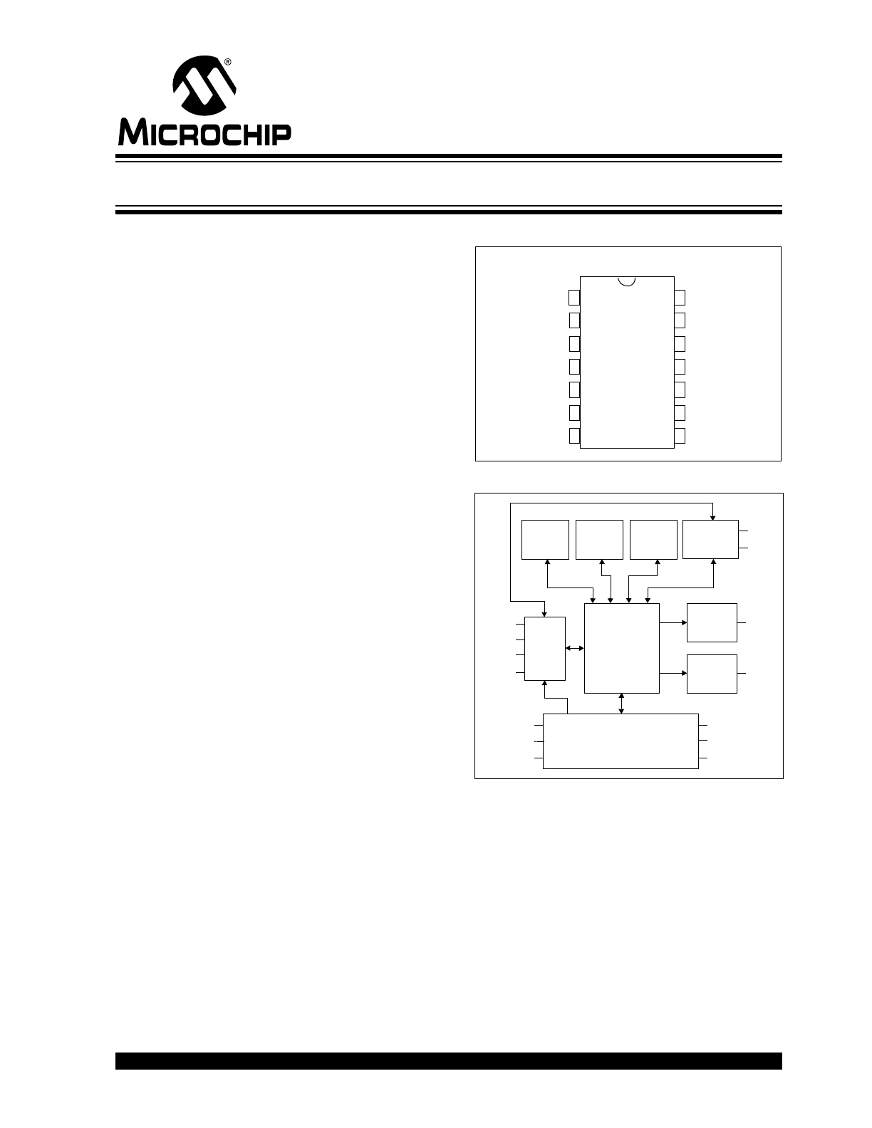
Package Types
Block Diagram
Typical Applications
• Passive entry systems
• Automotive remote entry systems
• Automotive alarm systems
• Automotive immobilizers
• Gate and garage openers
• Electronic door locks (Home/Office/Hotel)
• Burglar alarm systems
• Proximity access control
• Passive proximity authentication
8
14
1
2
3
4
13
12
11
S0
S1
S2
S3/RFEN
V
DD
LED
DATA
V
SS
PDIP, SOIC
HCS4
7
3
V
DDT
LCX
LCY
V
SST
LCCOM
LCZ
5
6
7
10
9
Wake-up
Control
Low
Voltage
Detector
3 Input Transponder
Circuitry
S0
S1
Internal
Oscillator
EEPROM
RESET and
Power
Control
V
DD
V
SS
Control
Logic
LED
DATA
S2
S3/
RFEN
LED
Driver
Data
Output
LCX
LCY
LCZ
V
DDT
LCCOM
V
SST
K
EE
L
OQ
®
3-Axis Transcoder

HCS473
DS40035D-page 2
Preliminary
2000-2013 Microchip Technology Inc.
Table of Contents
1.0
General Description ..................................................................................................................................................................... 3
2.0
Device Description ...................................................................................................................................................................... 5
3.0
Device Operation ....................................................................................................................................................................... 11
4.0
Programming Specification ....................................................................................................................................................... 37
5.0
Integrating the HCS473 Into A System ..................................................................................................................................... 39
6.0
Development Support................................................................................................................................................................. 43
7.0
Electrical Characteristics ........................................................................................................................................................... 49
8.0
Packaging Information................................................................................................................................................................ 57
INDEX .................................................................................................................................................................................................. 61
On-Line Support................................................................................................................................................................................... 62
Systems Information and Upgrade Hot Line ........................................................................................................................................ 62
Reader Response ................................................................................................................................................................................ 63
Product Identification System............................................................................................................................................................... 64
TO OUR VALUED CUSTOMERS
It is our intention to provide our valued customers with the best documentation possible to ensure successful use of your Microchip
products. To this end, we will continue to improve our publications to better suit your needs. Our publications will be refined and
enhanced as new volumes and updates are introduced.
If you have any questions or comments regarding this publication, please contact the Marketing Communications Department via
E-mail at docerrors@mail.microchip.com or fax the Reader Response Form in the back of this data sheet to (480) 792-4150.
We welcome your feedback.
Most Current Data Sheet
To obtain the most up-to-date version of this data sheet, please register at our Worldwide Web site at:
http://www.microchip.com
You can determine the version of a data sheet by examining its literature number found on the bottom outside corner of any page.
The last character of the literature number is the version number, (e.g., DS30000A is version A of document DS30000).
Errata
An errata sheet, describing minor operational differences from the data sheet and recommended workarounds, may exist for current
devices. As device/documentation issues become known to us, we will publish an errata sheet. The errata will specify the revision
of silicon and revision of document to which it applies.
To determine if an errata sheet exists for a particular device, please check with one of the following:
• Microchip’s Worldwide Web site; http://www.microchip.com
• Your local Microchip sales office (see last page)
• The Microchip Corporate Literature Center; U.S. FAX: (480) 792-7277
When contacting a sales office or the literature center, please specify which device, revision of silicon and data sheet (include liter-
ature number) you are using.
Customer Notification System
Register on our web site at www.microchip.com/cn to receive the most current information on all of our products.

2000-2013 Microchip Technology Inc.
Preliminary
DS40035D-page 3
HCS473
1.0
GENERAL DESCRIPTION
The HCS473 combines the patented K
EE
L
OQ
code
hopping technology and bi-directional transponder
challenge-and-response security into a single chip
solution for logical and physical access control.
The three-input transponder interface allows the com-
bination of three orthogonal transponder antennas,
eliminating the directionality associated with traditional
single antenna transponder systems.
When used as a code hopping encoder, the HCS473 is
well suited to keyless entry systems; vehicle and
garage door access in particular. The same HCS473
can also be used as a secure bi-directional transponder
for contactless authentication. These capabilities make
the HCS473 ideal for combined secure access control
and identification applications, dramatically reducing
the cost of hybrid transmitter/transponder solutions.
1.1
System Overview
1.1.1
KEY TERMS
The following is a list of key terms used throughout this
data sheet. For additional information on terminology,
please refer to the K
EE
L
OQ
introductory Technical Brief
(TB003).
• AGC - Automatic Gain Control.
• Anticollision - A scheme whereby transponders
in the same field can be addressed individually,
preventing simultaneous response to a command
(Section 3.2.1.4).
• Button Status - Indicates what button input(s)
activated the transmission. Encompasses the 4
button status bits S3, S2, S1 and S0 (Figure 3-2).
• Code Hopping - A method by which a code,
viewed externally to the system, appears to
change unpredictably each time it is transmitted
(Section 1.2.3).
• Code word - A block of data that is repeatedly
transmitted upon button activation (Figure 3-2).
• Crypto key - A unique and secret 64-bit number
used to encrypt and decrypt data. In a symmetri-
cal block cipher such as the K
EE
L
OQ
algorithm,
the encryption and decryption keys are equal and
will therefore be referred to generally as the
crypto key.
• Decoder - A device that decodes data received
from an encoder.
• Decryption algorithm - A recipe whereby data
scrambled by an encryption algorithm can be
unscrambled using the same crypto key.
• Device Identifier - 16-bit value used to uniquely
select one of multiple transponders for communi-
cation.
• Encoder - A device that generates and encodes
data.
• Encryption Algorithm - A recipe whereby data is
scrambled using a crypto key. The data can only
be interpreted by the respective decryption algo-
rithm using the same crypto key.
• IFF - Identify Friend or Foe, a classic authentica-
tion method (Section 3.2.3.3).
• Learn - Learning involves the receiver calculating
the transmitter’s appropriate crypto key, decrypt-
ing the received hopping code and storing the
serial number, synchronization counter value and
crypto key in EEPROM (Section 5.1). The
K
EE
L
OQ
product family facilitates several learning
strategies to be implemented on the decoder. The
following are examples of what can be done.
• Simple Learning
The receiver uses a fixed crypto key, common to
all components of all systems by the same manu-
facturer, to decrypt the received code word’s
encrypted portion.
• Normal Learning
The receiver uses information transmitted during
normal operation to derive the crypto key and
decrypt the received code word’s encrypted por-
tion.
• Secure Learn
The transmitter is activated through a special but-
ton combination to transmit a stored 60-bit seed
value used to derive the transmitter’s crypto key.
The receiver uses this seed value to calculate the
same crypto key and decrypt the received code
word’s encrypted portion.
• LF - Low Frequency. For HCS473 purposes, LF
refers to a typical 125 kHz frequency.
• Manufacturer’s code – A unique and secret 64-
bit number used to generate unique encoder
crypto keys. Each encoder is programmed with a
crypto key that is a function of the manufacturer’s
code. Each decoder is programmed with the man-
ufacturer code itself.
• Proximity Activation - A method whereby an
encoder automatically initiates a transmission in
response to detecting an inductive field
(Section 3.1.1.2).
• PKE - Passive Keyless Entry.
• RKE - Remote Keyless Entry.
• Transmission - A data stream consisting of
repeating code words.
• Transcoder - Device combining unidirectional
transmitter capabilities with bi-directional authenti-
cation capabilities.
• Transponder - A transmitter-receiver activated
for transmission by reception of a predetermined
signal.

HCS473
DS40035D-page 4
Preliminary
2000-2013 Microchip Technology Inc.
• Transponder Reader (Reader, for short) - A
device that authenticates a transponder using bi-
directional communication.
• Transport code - An access code, ‘password’
known only by the manufacturer, allowing write
access to certain secure device memory areas
(Section 3.2.3.2).
1.2
Encoder Overview
The HCS473 code hopping transcoder is designed
specifically for passive entry systems; particularly vehi-
cle access. The transcoder portion of a passive entry
system is integrated into a fob, carried by the user and
operated to gain access to a vehicle or restricted area.
The HCS473 is meant to be a cost-effective yet secure
solution to such systems, requiring very few external
components (Figure 2-1).
1.2.1
LOW-END SYSTEM SECURITY
RISKS
Most low-end keyless entry transmitters are given a
fixed identification code that is transmitted every time a
button is pushed. The number of unique identification
codes in a low-end system is usually a relatively small
number. These shortcomings provide an opportunity
for a sophisticated thief to create a device that ‘grabs’
a transmission and retransmits it later, or a device that
quickly ‘scans’ all possible identification codes until the
correct one is found.
1.2.2
HCS473 SECURITY
The HCS473, on the other hand, employs the K
EE
L
OQ
code hopping technology coupled with a transmission
length of 69 bits to virtually eliminate the use of code
‘grabbing’ or code ‘scanning’. The high security level of
the HCS473 is based on the patented K
EE
L
OQ
technol-
ogy. A block cipher based on a block length of 32 bits
and a key length of 64 bits is used. The algorithm
obscures the information in such a way that even if the
transmission’s pre-encrypted information differs by
only one bit from that of the previous transmission, sta-
tistically greater than 50 percent of the transmission’s
encrypted result will change.
1.2.3
HCS473 HOPPING CODE
The 16-bit synchronization counter is the basis behind
the transmitted code word changing for each transmis-
sion; it increments each time a button is pressed.
Once the device detects a button press, it reads the
button inputs and updates the synchronization counter.
The synchronization counter and crypto key are input
to the encryption algorithm and the output is 32 bits of
encrypted information. This encrypted data will change
with every button press, its value appearing externally
to ‘randomly hop around’, hence it is referred to as the
hopping portion of the code word. The 32-bit hopping
code is combined with the button information and serial
number to form the code word transmitted to the
receiver. The code word format is explained in greater
detail in Section 3.1.2.
1.3
Identify Friend or Foe (IFF)
Overview
Validation of a transponder first involves an authenti-
cating device sending a random challenge to the
device. The transponder then replies with a calculated
response that is a function of the received challenge
and its stored crypto key. The authenticating device,
transponder reader, performs the same calculation and
compares it to the transponder’s response. If they
match, the transponder is identified as valid and the
transponder reader can take appropriate action.
The HCS473’s IFF response is generated using one of
two possible crypto keys. The authenticating device
precedes the challenge with a three bit field dictating
which key to use in calculating the response.
The bi-directional communication path required for IFF
is typically inductive for short range (<10cm) transpon-
der applications with an inductive challenge and induc-
tive response. Longer range (~1.5m) passive entry
applications still transmit using the LF inductive path
but the response is transmitted RF.
2000-2013 Microchip Technology Inc.
Preliminary
DS40035D-page 5
HCS473
2.0
DEVICE DESCRIPTION
The HCS473 is designed for small package outline,
cost-sensitive applications by minimizing the number of
external components required for RKE and PKE appli-
cations.
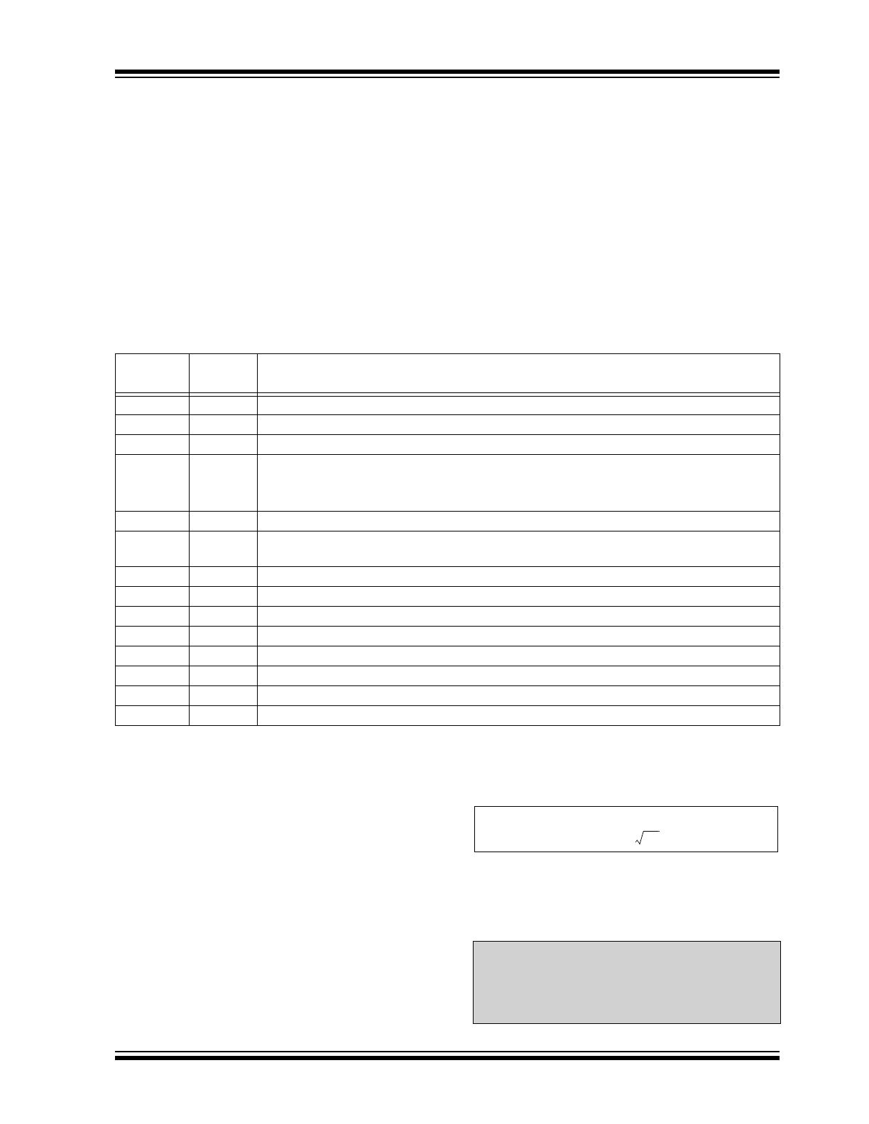
Figure 2-1 shows a typical 3-axis HCS473 RKE/PKE
application.
• The switch inputs have internal pull-down resis-
tors and integrated debouncing allowing a switch
to be directly connected to the inputs.
The transponder circuitry requires only the addition of
external LC-resonant circuits for inductive communica-
tion capability.
• The open-drain LED output allows an external
resistor for customization of LED brightness - and
current consumption.
• The DATA output can be directly connected to the
RF circuit or connected in conjunction with S3/
RFEN to a PLL.
2.1
Pinout Overview
A description of pinouts for the HCS473 can be found
in Table 2-1.
TABLE 2-1:
PINOUT SUMMARY
2.2
LF Antenna Considerations
A typical magnetic low frequency sensor (receiving
antenna) consists of a parallel inductor-capacitor circuit
that is sensitive to an externally applied magnetic sig-
nal. This LC circuit is tuned to resonate at the source
signal's base frequency. The real-time voltage across
the sensor represents the presence and strength of the
surrounding magnetic field. By amplitude modulating
the source's magnetic field, it is possible to transfer
data over short distances. This communication
approach is successfully used with distances up to 1.8
meters, depending on transmission strengths and sen-
sor sensitivity. Two key factors that greatly affect com-
munication range are:
1.
Sensor tuning
2.
A properly tuned sensor's relative sensitivity
An LC antenna’s component values may be initially cal-
culated using the following equation. “Initially” because
there are many factors affecting component selection.
It is not this data sheet’s purpose to present in-depth
details regarding LC antenna and their tuning. Please
refer to “Low Frequency Magnetic Transmitter Design
Application Note”, AN232, for appropriate LF antenna
design details.
Pin Name
Pin
Number
Description
S0
1
Button input pin with Schmitt Trigger detector and internal pull-down resistor (Figure 2-3).
S1
2
Button input pin with Schmitt Trigger detector and internal pull-down resistor (Figure 2-3).
S2
3
Button input pin with Schmitt Trigger detector and internal pull-down resistor (Figure 2-3).
S3/RFEN
4
Multi-purpose input/output pin (Figure 2-4).
• Button input pin with Schmitt Trigger detector and internal pull-down resistor.
• RFEN output driver.
V
DDT
5
Transponder supply voltage. Regulated voltage output for strong inductive field.
LCX
6
Sensitive transponder input X (Figure 2-7). A strong signal on this pin is internally regulated
and supplied on V
DD
for low-battery operation/recharging.
LCY
7
Sensitive transponder input Y (Figure 2-7)
LCZ
8
Sensitive transponder input Z (Figure 2-7)
LCCOM
9
Transponder bias output (Figure 2-7)
V
SST
10
Transponder ground reference, must be connected to V
SS
.
V
SS
11
Ground reference
DATA
12
Transmission data output (Figure 2-5)
LED
13
Open drain LED output (Figure 2-6)
V
DD
14
Positive supply voltage
Note:
Microchip also has a confidential Applica-
tion Note on Magnetic Sensors (AN832C).
Contact Microchip for a Non-Disclosure
Agreement in order to obtain this applica-
tion note.
2
F
1
LC
-----------
=
HCS473
DS40035D-page 6
Preliminary
2000-2013 Microchip Technology Inc.
FIGURE 2-1:
HCS473 3-AXIS
APPLICATION
FIGURE 2-2:
HCS473 1-AXIS
APPLICATION
FIGURE 2-3:
S0/S1/S2 PIN DIAGRAM
FIGURE 2-4:
S3/RFEN PIN DIAGRAM
FIGURE 2-5:
DATA PIN DIAGRAM
RF
Circuit
HCS473
S0
S1
S2
V
DDT
LCX
LCY
V
DD
LED
DATA
V
SS
V
SST
LCCOM
LCZ
S3/RFEN
1
F
100nF
V
DD
680pF
L
X
L
Y
L
Z
C
X
C
Y
C
Z
Note:
The 680pF capacitor prevents device instability - self
resonance.
RF
Circuit
HCS473
S0
S1
S2
V
DDT
LCX
LCY
V
DD
LED
DATA
V
SS
V
SST
LCCOM
LCZ
S3/RFEN
1
F
100nF
V
DD
660 pF
100
L
X
C
X
100
Note:
Connect unused LC antenna inputs to LCCOM
through a 100
resistor for proper bias conditions.
R
PD
S0, S1, S2
Inputs
S3 Input/
RFEN
RFEN Output
V
DD
R
PD
NFET
PFET
Note:
R
PD
is disabled when driving RFEN.
V
DD
RDATA
DATA
NFET
PFET
DATA OUT
Note:
RDATA is disabled when the DATA line is driven.
2000-2013 Microchip Technology Inc.
Preliminary
DS40035D-page 7
HCS473
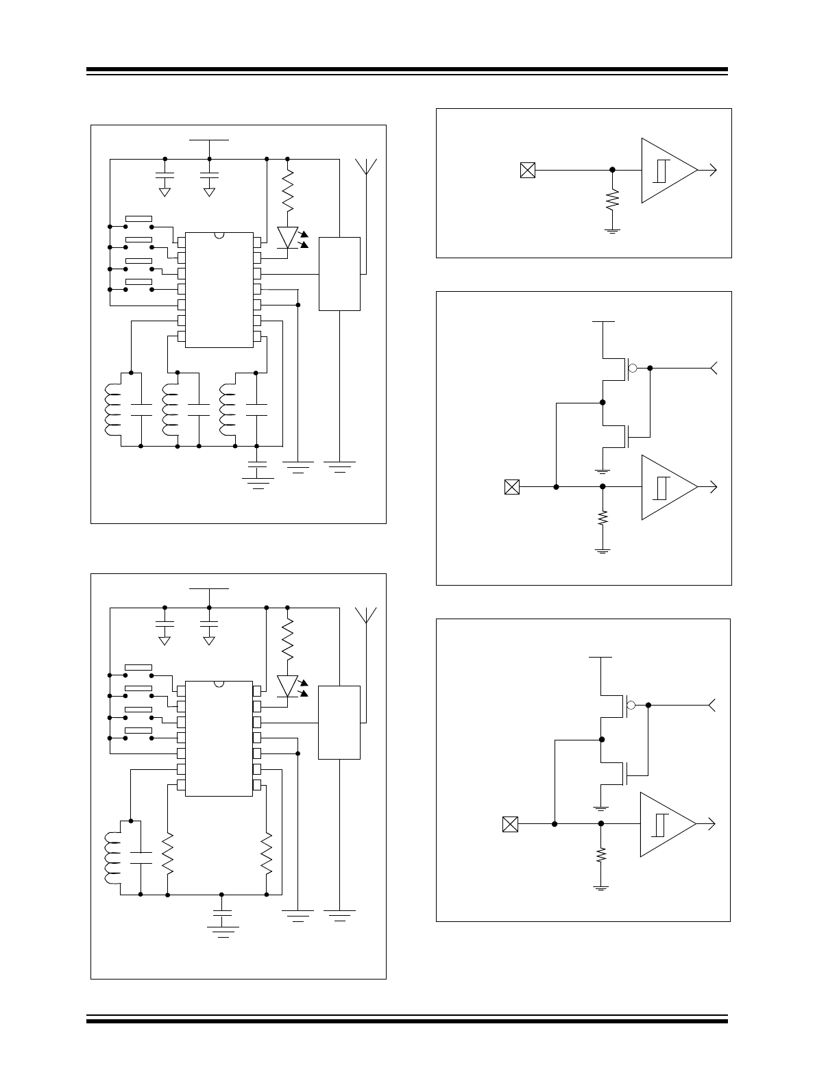
FIGURE 2-6:
LED PIN DIAGRAM
FIGURE 2-7:
LCCOM/LCX/LCY/LCZ/
VSST PIN DIAGRAM
2.3
Architectural Overview
2.3.1
WAKE-UP LOGIC
The HCS473 automatically goes into a low-power
Standby mode once connected to a supply voltage.
Power is supplied to the minimum circuitry required to
detect a wake-up condition; button activation or LC sig-
nal detection.
The HCS473 will wake from Low-power mode when a
button input is pulled high or a signal is detected on a
LC low frequency antenna input pin. Waking involves
powering the main logic circuitry that controls device
operation. The button and transponder inputs are then
sampled to determine which input activated the device.
A button input activation places the device into Encoder
mode. A signal detected on the transponder input
places the device into Transponder mode. Encoder
mode has priority over Transponder mode such that
communication on the transponder input would be
ignored or perhaps interrupted if it occurred simulta-
neously to a button activation; ignored until the button
input is released.
2.3.2
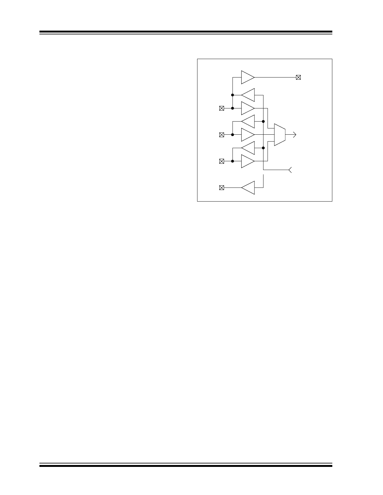
ENCODER INTERFACE
Using the four button inputs, up to 15 unique control
codes may be transmitted.
LED
HV
Detect
Program
Weak
LED
V
DD
Mode
LCX/LCY/
LCZ Inputs
RECTIFIER and
REGULATOR
V
SST
10V
100
LC
Input
AMP
DET
and
DAMP
LCX
only
10V
100
BIAS
CURRENT
LCCOM
CLAMP
R
DAMP
Note:
S3 may not be used as a button input if the
RFEN option is enabled.
HCS473
DS40035D-page 8
Preliminary
2000-2013 Microchip Technology Inc.
2.3.3
TRANSPONDER INTERFACE
The transponder interface on the HCS473 consists of
the following:
• The internal transponder circuitry has separate
power supply (V
DDT
) and ground (V
SST
) connec-
tions.
- The V
DDT
pin supplies power to the transpon-
der circuitry and also outputs a regulated volt-
age if the LCX antenna input is receiving a
strong signal; transponder is placed in a
strong LF field.
- The V
SST
pin supplies the ground reference
to the transponder circuitry and must be con-
nected to the V
SS
pin.
• LF input amplifier and envelope detector to detect
and shape the incoming low frequency excitation
signal.
• Three sensitive transponder inputs with over-volt-
age protection (LCX, LCY, LCZ).
• Incoming LF energy rectification and regulation on
the LCX input to supplement the supply voltage in
low-battery transponder instances.
• 10V zener input protection from excessive
antenna voltage resulting when proximate to very
strong magnetic fields.
• LCCOM pin used to bias the transponder reso-
nant circuits for best sensitivity.
• LF antenna clamping transistors for inductive
responses back to the transponder reader. The
antenna ends are shorted together, ‘clamped’,
dissipating the oscillatory energy. The reader
detects this as a momentary load on its excitation
antenna.
• Damping transistors to increase LF communica-
tion reliability when using high Q-factor LC anten-
nae.
The LCCOM pin functions to bias the LCX, LCY, and
LCZ AGC amplifier inputs. The amplifier gain control
sets the optimum level of amplification in respect to the
incoming signal strength. The signal then passes
through an envelope detector before interpretation in
the logic circuit.
A block diagram of the transponder circuit is shown in
Figure 2-8.
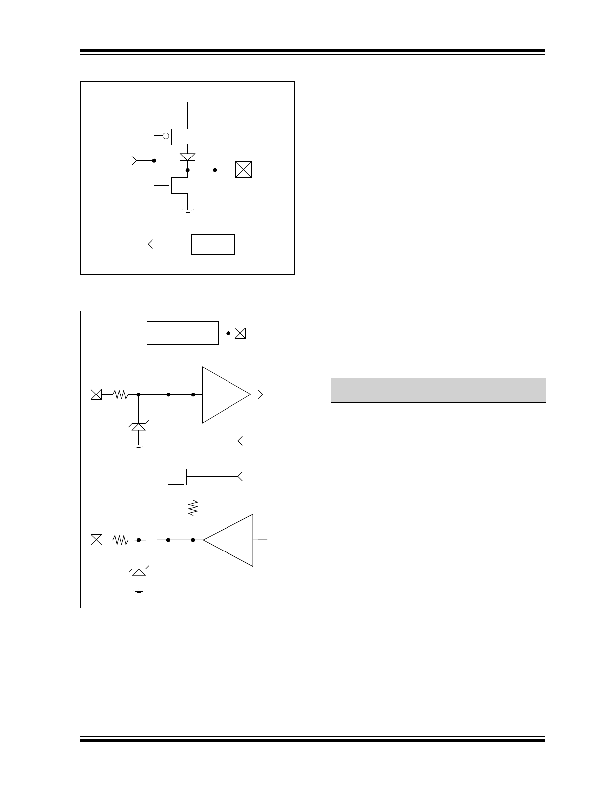
FIGURE 2-8:
HCS473 TRANSPONDER
CIRCUIT
2.3.4
INTERNAL EEPROM
The HCS473 has an on-board non-volatile EEPROM
which is used to store:
• configuration options
- encryption keys
- serial number
- vehicle ID’s
- baud rates
- ... see Section 3.1.4 and Section 3.2.1
• 64 bits of user memory
• synchronization counter.
All options are programmable during production, but
many of the security related options are programmable
only during production and are further read protected.
The user area allows storage of general purpose infor-
mation and is accessible only through the transponder
communication path.
During every EEPROM write, the device ensures that
the internal programming voltage is at an acceptable
level prior to performing the EEPROM write.
Rectifier/
Regulator
V
CCT
Noise
Filter
Signal In
Damp/Clamp
Control
LCX
LCY
LCZ
LCCOM
2000-2013 Microchip Technology Inc.
Preliminary
DS40035D-page 9
HCS473
2.3.5
INTERNAL RC OSCILLATOR
The HCS473 runs on an internal RC oscillator. The
internal oscillator may vary ±10% over the device’s
rated voltage and temperature range for commercial
temperature devices. A certain percentage of indus-
trial temperature devices vary further on the slow side,
-20%, when used at higher voltages (V
DD
> 3.5V) and
cold temperature. The LF and RF communication
timing values are subject to these variations.
2.3.6
LOW VOLTAGE DETECTOR
The HCS473’s battery voltage detector detects when
the supply voltage drops below a predetermined value.
The value is selected by the Low Voltage Trip Point
Select (VLOWSEL) configuration option (Section 3.3).
The low voltage detector result is included in encoder
transmissions (VLOW) allowing the receiver to indicate
when the transmitter battery is low (Section 3.1.4.6).
The HCS473 also indicates a low battery condition by
changing the LED operation (Section 3.1.5).
2.3.7
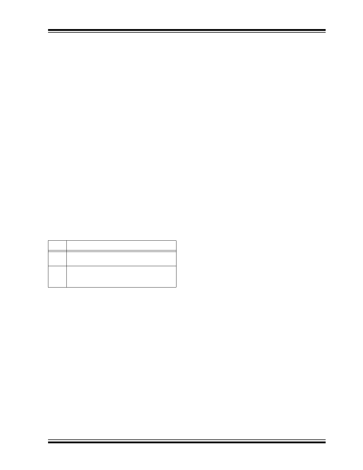
THE S3/RFEN PIN
The S3/RFEN pin may be used as a button input or RF
enable output to a compatible PLL. Select between S3
button input and RFEN functionality with the RFEN
configuration option (Table 2-2).
TABLE 2-2:
RFEN OPTION
RFEN
Resulting S3/RFEN Configuration
0
S3 button input pin with Schmitt Trigger
detector and internal pull-down resistor.
1
RFEN output driver.
S3 may not be used as a button input if the
RFEN option is enabled

HCS473
DS40035D-page 10
Preliminary
2000-2013 Microchip Technology Inc.
NOTES: