

2016 Microchip Technology Inc.
DS20005639A-page 1
HV7321
Features
• Power Sequencing Free 5 Output Levels
including RTZ (Return-to-Zero)
• -44 dB Single-Cycle Pulse-Inversion Second
Harmonic Distortion (HD2) at 5 MHz
• Output Voltage up to ±80V
• ±2.5A Peak Output Current
• ±300 mA Current from V
PP1
/V
NN1
in CW Mode-0
• Integrated T/R Switch & RX Damper Switch
• Bleeder Switches Achieve True Zero during RTZ
• Supports Both Transparent and Re-Timing Mode
• Re-Timing Clock Frequency Supports up to
220 MHz
• Built-In Output Protection Diodes and Clamp
Diodes
• +2.5/+3.3V Input Logic
• Built-In CW Switches to Pair with External CW
Transmitters (CW Mode-1)
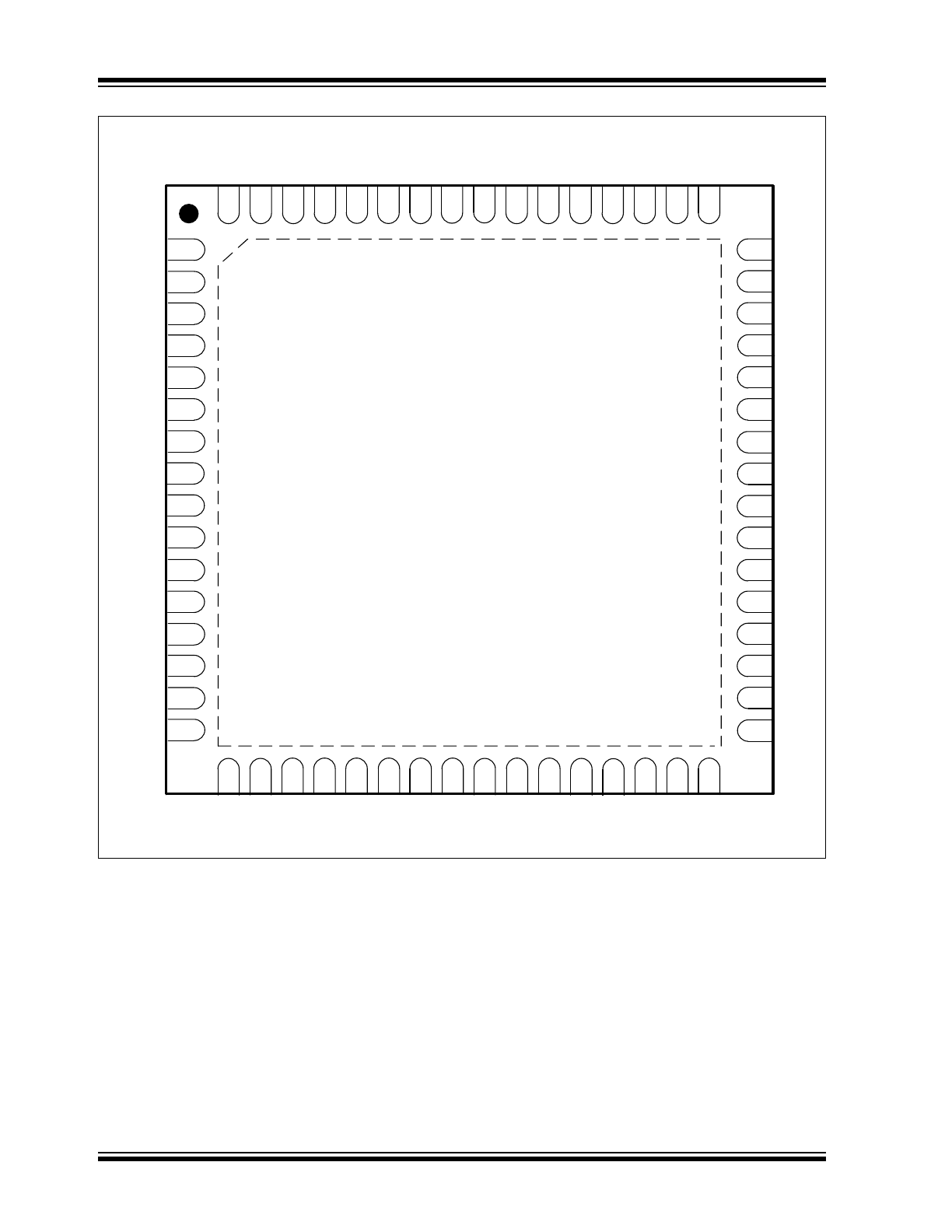
• 9 mm x 9 mm 64-Lead VQFN Package
Applications
• Medical Ultrasound Imaging Systems
• NDT Ultrasound
• Piezoelectric or Capacitive Transducer Drivers
General Description
The HV7321 is a 4-channel, 5-level, ultrasound
transmitter with built-in T/R switches, output protection
diodes and clamp diodes. The HV7321 can provide up
to ±2.5A and the output voltage swing can be up to
±80V. The HV7321 supports both Transparent and
Re-Timing mode. The re-timing clock frequency can
support up to 220 MHz. The re-timing feature helps
reduce the output jitter introduced by the driving the
field-programmable gate array (FPGA).
The HV7321 has two different modes for
CW transmission, CW-Mode 0 and CW-Mode 1.
In CW-Mode 0 (Mode = 0, PWS = 0), the V
PP1
and
V
NN1
rails are used for CW transmission. The output
current is reduced in CW Mode-0.
In CW-Mode 1, the HV7321 accepts the output of an
external CW beamformer as CW source.
The HV7321 is LVCMOS 2.5V/3.3V input compatible,
which can be interfaced with the FPGA directly.
The HV7321 is available in a 9 mm x 9 mm 64-Lead
VQFN package.
4-Ch. 5-Level ±80V High-Voltage Ultrasound Pulser with T/R Switches
HV7321
DS20005639A-page 2
2016 Microchip Technology Inc.
Package Types
65
V
SUB
63
64
60
61
59
58
54
55
56
57
62
50
51
52
53
49
PO
S0
NE
G
0
SE
L0
MO
DE
V
DD
GN
D
V
GN
V
PP0
V
PP0
C
PF
0
C
NF
0
V
NN
0
V
NN
0
V
NN
2
V
NN
1
C
NF
1
15
16
12
13
11
10
6
7
8
9
14
2
3
4
5
1
CW
IN0
SEL1
NEG1
POS1
PWS
CLK
GND
V
LL
REN
NEG2
CW
IN2
SEL3
POS2
20
19
22
21
25
24
26
27
31
30
29
28
23
32
18
17
CW
IN1
OEN
SEL2
NE
G
3
PO
S3
CW
IN
3
OT
P
N
V
DD
GN
D
V
GP
V
PP0
C
PF
0
V
NN
0
V
NN
2
V
NN
1
C
NF
1
V
PP0
C
NF
0
V
NN
0
36
35
38
37
41
40
42
43
47
46
45
44
39
48
34
33
C
PF1
V
PP1
TX0
RX0
R
GND
RX1
C
NEG
R
GND
TX3
C
PF1
V
PP1
RX3
RX2
TX2
C
POS
TX1
2016
Microchip Technology Inc.
D
S
20005639A-
page 3
HV7321
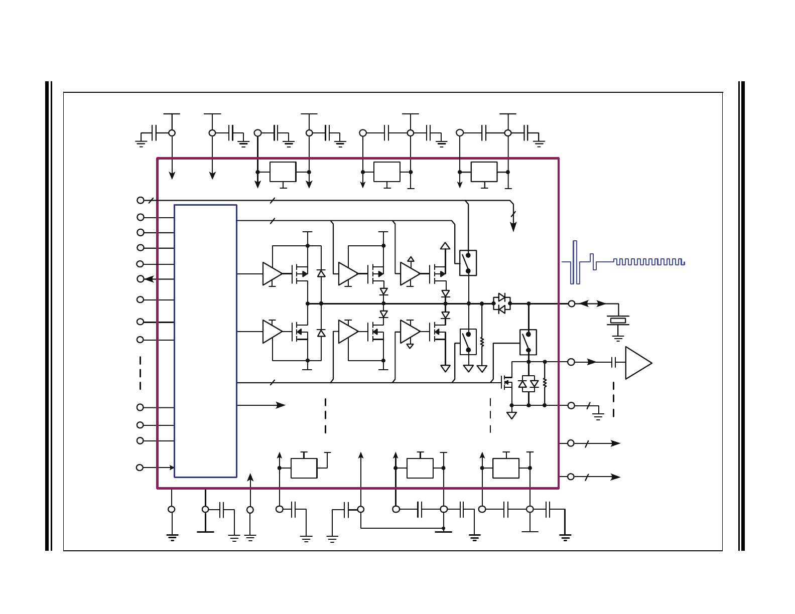
HV7321 – Block Diagram
Rb
OEN
POS3
NEG3
SEL3
CLK
X0
RX0
+2.5V/3V
+5V
-10V
GND
V
GN
V
SUB
C
NEG
V
NN2
C
NF0
V
NN0
C
NF1
V
NN1
TX0
RX0
R
GND
TX1,2,3
V
LL
V
DD
C
POS
V
GP
C
PF0
V
PP0
C
PF1
V
PP1
2 µF
2 µF
V
PF1
V
GN
V
PP1
V
PP0
V
NEG
GND V
GN
V
NF1
V
NN2
V
PP0
SUB
V
POS
To Ch.
1-3
0 to +80V
0 to +80V
0 to -80V
0 to -80V
2 µF
1 µF
2 µF
2 µF
2 µF
2 µF
2 µF
100V
100V
V
GN
V
PF0
GND
1 µF
1 µF
100V
2 µF
1 µF
100V
2 µF
2 µF
100V
V
NF0
V
GP
V
NN0
V
GP
V
NN1
V
PP1
to
CWSW1-3
CWSW0
V
PF0
V
NF0
V
PF0
V
NEG
V
NF1
V
POS
V
NN0
V
NN1
RTZSW0
TRSW0
Rb
RXDMP0
R
GND
1 of 4 channels
+10V
LR
V
POS
LR
V
PF0
LR
V
PF1
RX1,2,3
LR
V
NEG
LR
V
NF0
LR
V
NF1
SEL0
NEG0
POS0
OTP
N
PWS
REN
MODE
CW
IN0-3
Logic
and
Retiming
HV7321
DS20005639A-page 4
2016 Microchip Technology Inc.
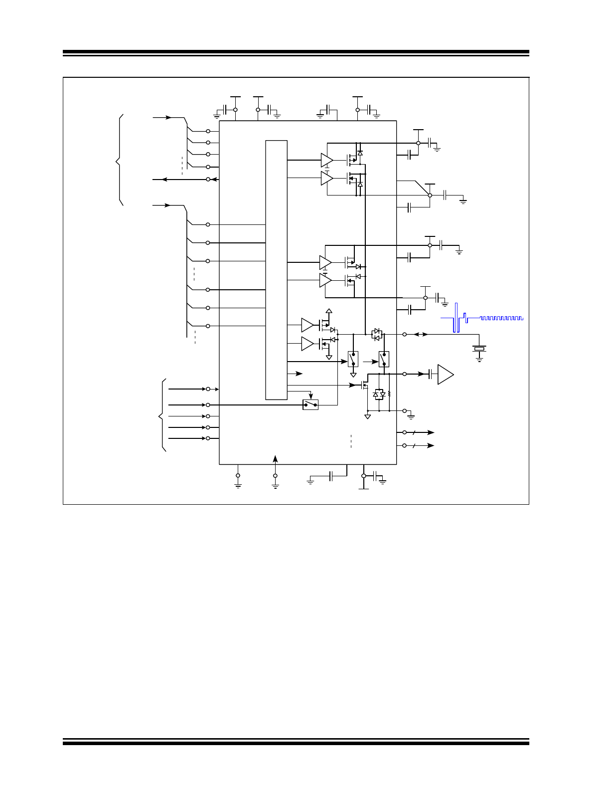
HV7321 – Typical Application Circuit
X0
+80V
V
PF1
V
NN1
TX0
-60V
V
PP0
V
NN0
-80V
+60V
1 of 4 Channels
V
DD
CW
IN3
GND
+2.5V
V
LL
PWS
POS3
V
SUB
MODE
REN
TX1-3
RX1-3
RX0
R
GND
RTZSW
CWSW
RXDMP
TRSW
V
GP
-10V
OEN
to other ICs
CTRN[3:0]
OTP
N
DT[63:0]
C
LL
= 2 µF 10V
C
DD
= 2µF 10V
C
GP
= 2 µF 16V
C
PP0
= 2 µF 100V
C
PP1
= 2 µF 100V
C
NN1
= 2 µF 100V
C
GN
= 2 µF 16V
Connect to a low-voltage
CW source
(such as the MD1730)
C
CPOS
= 1µF 10V
C
POS
C
PF0
C
PF1
C
CPF1
= 2 µF 10V
C
NF0
C
CNEG
= 1 µF 10V
C
NEG
C
NF1
C
CNF1
= 2 µF 10V
C
NN0
= 2 µF 100V
C
CNF0
= 2 µF 10V
C
CPF1
= 2 µF 10V
V
NN2
V
NF1
TXFPGA I/Os
+5V
+10V
V
PP1
RX0
V
GN
R
GND
SUB
TRSW
Decode
&
Level
Shift
V
PF0
V
NF0
CW
IN2
CW
IN1
CW
IN0
CLK
NEG3
SEL3
POS0
NEG0
SEL0
OTP
N
For CW Mode-1
2016 Microchip Technology Inc.
DS20005639A-page 5
HV7321
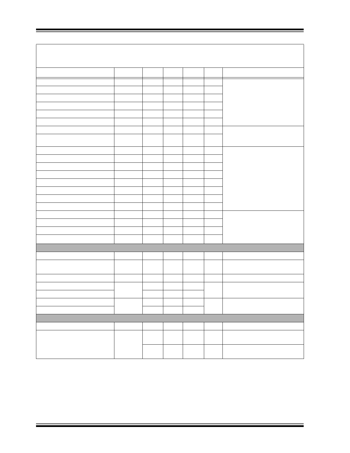
1.0
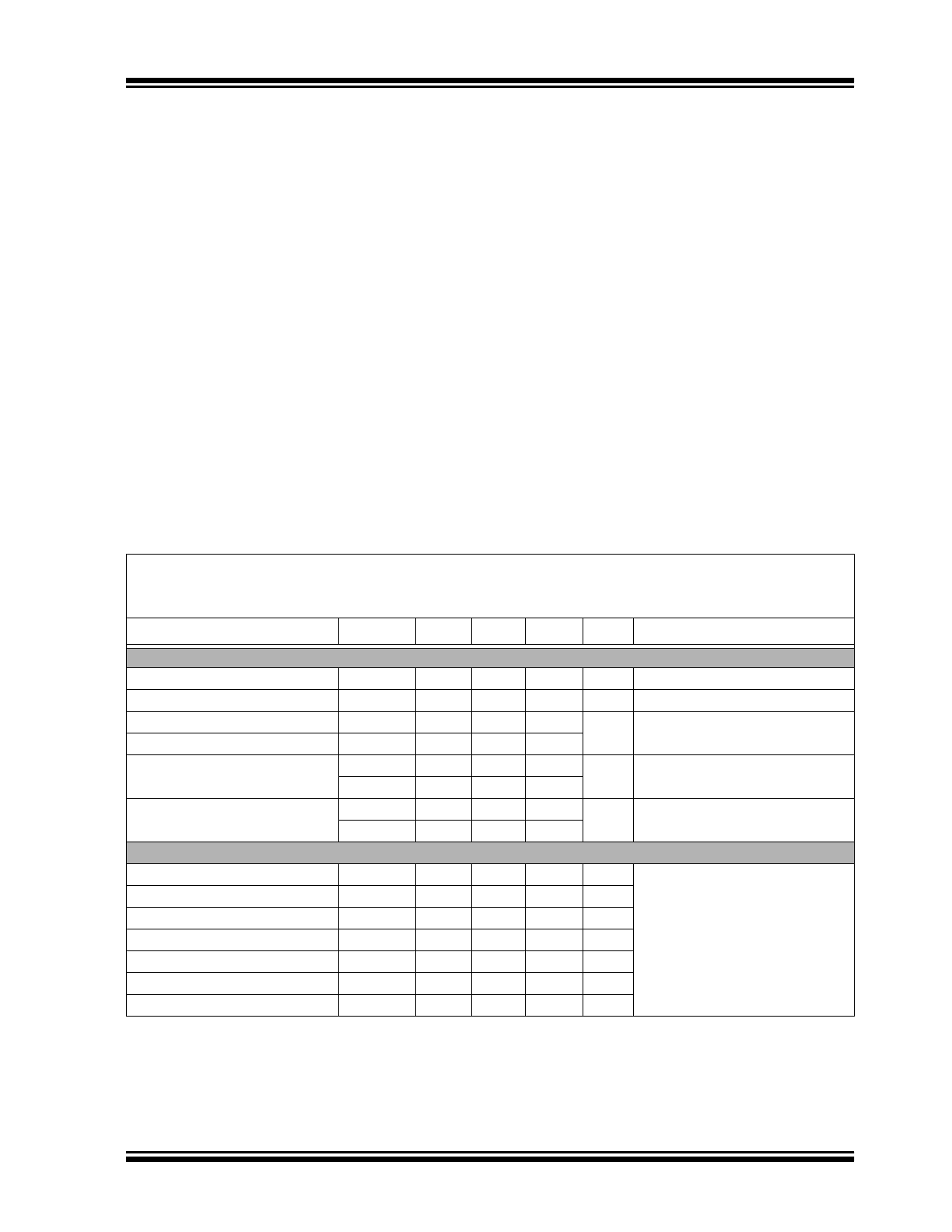
ELECTRICAL CHARACTERISTICS
Absolute Maximum Ratings †
Positive logic supply (V
LL
).......................................................................................................................... -0.5V to +5.5V
All I/O & CLK pin voltage (V
IO
)................................................................................................................... -0.5V to +5.5V
Positive voltage supply (V
DD
)..................................................................................................................... -0.5V to +5.5V
Positive gate driver supply (V
GP
) ............................................................................................................. -0.5V to +13.5V
Negative gate driver supply (V
GN
) ........................................................................................................... -13.5V to +0.5V
High voltage positive supply (V
PP0,1
) .......................................................................................................... -1.0V to +85V
High voltage negative supply (V
NN0,1,2
)...................................................................................................... -85V to +1.0V
CW input voltage (V
CWIN
) .......................................................................................................................... -7.5V to +7.5V
TX pin voltage (V
TX
)..................................................................................................................................... -85V to +85V
RX pin to GND voltage (V
RX
) .......................................................................................................................±0.7 to ±1.4V
Operating temperature ................................................................................................................................ 0°C to +85°C
Storage temperature ...............................................................................................................................-55°C to +150°C
Maximum junction temperature............................................................................................................................ +130°C
Maximum not-latch-up current ........................................................................................................................... +100 mA
ESD Rating CW
IN
,TX, V
PP
, V
NN
pins......................................................................................................................±500V
ESD Rating – all other pins ....................................................................................................................................... ±2kV
† Notice:
Stresses above those listed under “Maximum Ratings” may cause permanent damage to the device. This is a
stress rating only and functional operation of the device at those or any other conditions above those indicated in the
operational sections of this specification is not intended. Exposure to maximum rating conditions for extended periods
may affect device reliability.
ELECTRICAL CHARACTERISTICS
Electrical specifications:
V
LL
= +2.5V, V
DD
= +5.0V, V
PP0,1
= +80V, V
NN0,1,2
= -80V, V
GP
= +10V, V
GN
= -10V,
V
SUB
= 0V, PWS = OEN = REN = 1, T
A
= 25°C, unless otherwise specified. Parameters in Bold apply over the
operating temperature range of T
A
= T
J
= 0 to +85°C.
Parameter
Sym.
Min.
Typ.
Max.
Unit
Conditions
Operating Supply Voltages
Positive Logic Supply
V
LL
2.25
2.50
3.60
V
Note 1
Positive Voltage Supply
V
DD
4.75
5.0
5.25
V
Note 1
Positive Gate Driver Supply
V
GP
8.0
10
12
V
Note 1
See
Table 3-1
.
Negative Gate Driver Supply
V
GN
-12
-10
-8.0
High Voltage Positive Supply
V
PP0
0
—
80
V
Note 1
Must be V
PP0
≥ V
PP1
V
PP1
0
—
80
High Voltage Negative Supply
V
NN0
-80
—
0
V
Note 1
Must be V
NN0
V
NN1
V
NN1
-80
—
0
Operating Supply Current
V
LL
Quiescent Current
I
LLQ
—
0.06
0.7
μA
OEN = REN = 0
V
DD
Quiescent Current
I
DDQ
—
30
80
µA
V
PP0
Quiescent Current
I
PP0Q
—
0.37
6
µA
V
NN0
Quiescent Current
I
NN0Q
-9
-0.78
—
µA
V
PP1
Quiescent Current
I
PP1Q
—
0.44
10
µA
V
NN1
Quiescent Current
I
NN1Q
-10
-1.46
—
µA
V
NN2
Quiescent Current
I
NN2Q
-7
-3.84
—
µA
Note 1:
Characterized only; not 100% tested in production.
2:
Design guidance only.
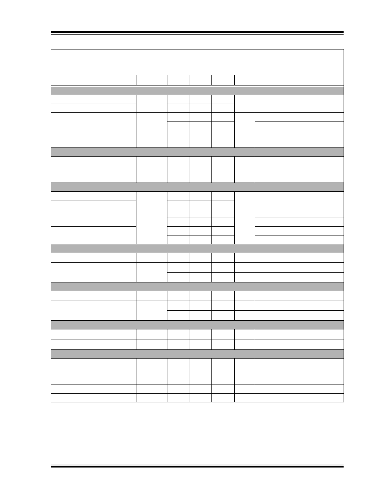
HV7321
DS20005639A-page 6
2016 Microchip Technology Inc.
V
DD
Current
I
DDEN
—
0.9
1.0
mA
f = 0 MHz
f
CLK
= 0 MHz
MODE = 0 or 1
V
PP0
Current
I
PP0EN
—
0.1
0.13
mA
V
NN0
Current
I
NN0EN
-0.12
-0.1
—
mA
V
PP1
Current
I
PP1EN
—
0.1
0.13
mA
V
NN1
Current
I
NN1EN
-0.12
-0.1
—
mA
V
NN2
Current
I
NN2EN
-0.05
-0.03
—
mA
V
LL
Current with Re-Timing
I
LLRT
—
0.11
0.3
mA
f
CLK
= 80 MHz
TX one-channel output, no load,
continuous,
Note 1
V
DD
Current with Re-Timing
I
DDRT
—
7.08
8
mA
V
LL
Max. Current of SEL = 0/1
I
LL5
—
23
40
μA
CLK
= 0
PWS = 1
MODE = 0
I
PP05
/I
NN05
and I
PP15
/I
NN15
are
calculated using TX one channel
output continuous, no load, at
5 MHz.
V
DD
Max. Current of SEL = 0/1
I
DD5
—
1.5
1.7
mA
V
GP
Max. Current of SEL = 0/1
I
GP5
—
2.6
4
mA
V
GN
Max. Current of SEL = 0/1
I
GN5
-14
-9
—
mA
V
PP0
Current of SEL = 0
(
1
)
I
PP05
—
136
146
mA
V
NN0
Current of SEL = 0
(
1
)
I
NN05
-132
-125
—
mA
V
PP1
Current of SEL = 1
(
1
)
I
PP15
—
148
158
mA
V
NN1
Current of SEL = 1
(
1
)
I
NN15
-150
-143
—
mA
V
GP
Current of SEL = 1
I
GPCW
—
1.0
2.0
mA
TX one-channel output 5 MHz,
continuous, no load
V
PP1
/V
NN1
= ±5V
PWS = MODE = 0
CW Mode-0,
Note 1
V
GN
Current of SEL = 1
I
GNCW
-8.0
-5.0
—
mA
V
PP1
Current of SEL = 1
I
PP1CW
—
17
26
mA
V
NN1
Current of SEL = 1
I
NN1CW
-20
-15
—
mA
CWSW High-Voltage Analog Switch
CW Switch Input Voltage
V
CWIN0–3
-7.0
—
+7.0
V
CWSW Analog Switch
On-Resistance
(
1
)
R
CWSW
—
26.5
35
Ω
I
CWSW
= ±100 mA
TRSW Off Withstand Voltage
V
CWSW
-80
—
+80
V
I
SW
= ±1.0 μA
CWSW Off Capacitance to GND
C
CWSW
—
5.0
—
pF
MODE = 1, 1 MHz, 0 dBm,
DC 0V,
Note 1
CWSW On Capacitance to GND
—
60
—
CWSW Switching On Time
t
CWSW
—
800
1100
ns
50% MODE rise to CWSW on/off
Note 1
CWSW Switching Off Time
—
66
90
TX Output P-Channel MOSFET on V
PP0
On-Resistance
R
ON_P0
—
8.5
19
Ω
I
SD
= 100 mA
Peak Output Current
I
OUT_P0
1
1.5
—
A
V
PP0
= +25V, R
L
= 1.0Ω to GND
Note 1
2.0
2.8
—
A
V
PP0
= +80V, R
L
= 1.0Ω to GND
Note 1
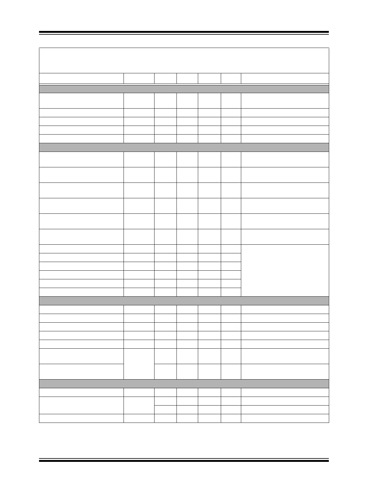
ELECTRICAL CHARACTERISTICS (CONTINUED)
Electrical specifications:
V
LL
= +2.5V, V
DD
= +5.0V, V
PP0,1
= +80V, V
NN0,1,2
= -80V, V
GP
= +10V, V
GN
= -10V,
V
SUB
= 0V, PWS = OEN = REN = 1, T
A
= 25°C, unless otherwise specified. Parameters in Bold apply over the
operating temperature range of T
A
= T
J
= 0 to +85°C.
Parameter
Sym.
Min.
Typ.
Max.
Unit
Conditions
Note 1:
Characterized only; not 100% tested in production.
2:
Design guidance only.
2016 Microchip Technology Inc.
DS20005639A-page 7
HV7321
TX Output P-Channel MOSFET on V
PP1
On-Resistance at PWS = 1
R
ON_P1
—
16
21
Ω
I
SD
= 100 mA
On-Resistance at PWS = 0
—
33
43
Peak Output Current at PWS = 1
(
1
)
I
OUT_P1
0.8
1.0
—
A
V
PP0,1
= +25V, R
L
= 1.0Ω to GND
1.5
1.75
—
V
PP0,1
= +80V, R
L
= 1.0Ω to GND
Peak Output Current at PWS = 0
(
1
)
0.4
0.5
—
V
PP0,1
= +25V, R
L
= 1.0Ω to GND
0.8
0.95
—
V
PP0,1
= +80V, R
L
= 1.0Ω to GND
TX Output N-Channel MOSFET on V
NN0
On-Resistance
R
ON_N0
—
8
10
Ω
I
SD
= 100 mA
Peak Output Current
(
1
)
I
OUT_N0
-1.4
-1.7
—
A
V
NN0
= -25V, R
L
= 1.0Ω to GND
-2.0
-2.3
—
A
V
NN0
= -80V, R
L
= 1.0Ω to GND
TX Output N-Channel MOSFET on V
NN1
On-Resistance at PWS = 1
R
ON_N1
—
11
13
Ω
I
SD
= 100 mA
On-Resistance at PWS = 0
—
36
45
Peak Output Current at PWS = 1
(
1
)
I
OUT_N1
—
-1.2
-1.0
A
V
NN0,1
= -25V, R
L
= 1.0Ω to GND
—
-1.6
-1.3
V
NN0,1
= -80V, R
L
= 1.0Ω to GND
Peak Output Current at PWS = 0
(
1
)
—
-0.4
-0.3
V
NN0,1
= -25V, R
L
= 1.0Ω to GND
—
-0.55
-0.4
V
NN0,1
= -80V, R
L
= 1.0Ω to GND
TX Damping P-Channel MOSFET on
GND
On-Resistance
R
ON_PDMP
—
7.0
16
Ω
I
SD
= 100 mA
Peak Output Current
(
1
)
I
OUT_PDMP
2.3
2.7
—
A
R
L
= 1.0Ω from -25V to TX
2.3
2.8
—
A
R
L
= 1.0Ω from -80V to TX
TX Damping N-Channel MOSFET on
GND
On-Resistance
R
ON_NDMP
—
7.0
16
Ω
I
SD
= 100 mA
Peak Output Current
(
1
)
I
OUT_NDMP
—
-2.0
-1.8
A
R
L
= 1.0Ω from +25V to TX
—
-2.3
-2.0
A
R
L
= 1.0Ω from +80V to TX
RTZSW Auto Bleed High-Voltage Analog Switch
RTZSW On-Resistance
(
1
)
R
RTZSW
—
238
270
Ω
I
SD
= ±1.0 mA
RTZSW Off Withstand Voltage
(
1
)
V
RTZSW
-80
—
+80
V
I
SW
= ±100 μA
TX OUTPUT Isolation Diodes and Bleed Resistor
Diode Forward Voltage
V
F
—
0.96
1.9
V
I
FM
= 300 mA,
Note 1
Forward Continuous Current
I
FM
—
300
—
mA
Note 2
Peak Forward Pulse Current
I
FSM
—
3.0
—
A
PW = 50 ns,
Note 2
Total Capacitance of 2-diode
C
T
—
3.5
—
pF
at 1 MHz, 1 dBm, 0V DC,
Note 2
TX/RX Bleed Resistor to GND
R
b
11
15
20
kΩ
Note 1
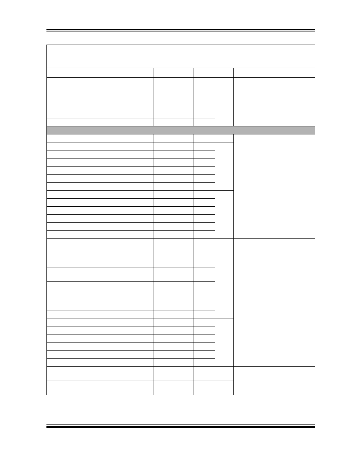
ELECTRICAL CHARACTERISTICS (CONTINUED)
Electrical specifications:
V
LL
= +2.5V, V
DD
= +5.0V, V
PP0,1
= +80V, V
NN0,1,2
= -80V, V
GP
= +10V, V
GN
= -10V,
V
SUB
= 0V, PWS = OEN = REN = 1, T
A
= 25°C, unless otherwise specified. Parameters in Bold apply over the
operating temperature range of T
A
= T
J
= 0 to +85°C.
Parameter
Sym.
Min.
Typ.
Max.
Unit
Conditions
Note 1:
Characterized only; not 100% tested in production.
2:
Design guidance only.
HV7321
DS20005639A-page 8
2016 Microchip Technology Inc.
TRSW and RXDMP Switches
TRSW Analog Switch
On-Resistor
R
TRSW
—
18
22
Ω
I
TRSW
= ±1.0 mA
Note 1
TRSW Off Withstand Voltage
V
TRSW
-80
—
+80
V
I
SW
= ±100 μA,
Note 1
RX to GND Protection Diode
V
F
—
1.5
2.2
V
I
F
= ±100 mA,
Note 1
RXDMP Switch On-Resistance
R
RXDMP
—
17
21
Ω
I
SD
= ±1.0 mA,
Note 1
RX Pin to GND Capacitance
C
RXG
—
—
7.0
pF
1 MHz, 1 dBm, 0V DC,
Note 2
Built-In Gate Drive Voltage Linear Regulators
Output P-Channel Gate Drive
Voltage Referenced to V
PP0
V
PF0
-5.2
-4.6
-3.8
V
V
GN
- V
PP0
< -10V
Output P-Channel Gate Drive
Voltage Referenced to V
PP1
V
PF1
-5.2
-4.6
-3.8
V
V
GN
- V
PP1
< -10V
Output N-Channel Gate Drive
Voltage Referenced to V
NN0
V
NF0
3.3
4.2
5.2
V
V
GP
- V
NN0
> 10V
Output N-Channel Gate Drive
Voltage Referenced to V
NN1
V
NF1
3.3
4.2
5.2
V
V
GP
- V
NN1
> 10V
Output N-Channel Gate Drive
Voltage Referenced to GND
V
POS
3.2
4.2
5.2
V
Output P-Channel Gate Drive
Voltage Referenced to GND
V
NEG
-5.2
-4.5
-3.8
V
Dropout Voltage of (V
PP0
- V
GN
) V
DOPF0
-2.9
-2.6
-2.4
V
Dropout Voltage of (V
PP1
- V
GN
)
V
DOPF1
-2.9
-2.6
-2.4
V
Dropout Voltage of (V
GP
- V
NN0
)
V
DONF0
3.0
3.3
3.6
V
Dropout Voltage of (V
GP
- V
NN1
)
V
DONF1
3.0
3.3
3.6
V
Dropout Voltage of (V
NEG
- V
GN
)
V
DONEG
2.9
3.3
3.5
V
Dropout Voltage of (V
GP
- V
POS
)
V
DOPOS
-2.8
-2.6
-2.4
V
Logic & Clock Input Characteristics
Input Logic Low Voltage
V
IL
0
—
0.2 V
LL
V
Input Logic High Voltage
V
IH
0.8 V
LL
—
V
LL
V
Input Logic Low Current
I
IL
-1.0
—
—
μA
Note 1
Input Logic High Current
I
IH
—
—
1.0
μA
Note 1
Input Capacitance
C
IN
—
2.0
3.0
pF
Note 2
OEN Switching On Time
t
OEN
—
200
—
µs
50% OEN rise to TX ready,
Note 2
OEN Switching Off Time
—
20
—
ns
50% OEN fall to TX all output
FETs on HV rails are off,
Note 1
Thermal protection OTP
N
& UVLO
OTP
N
Output Max. Pull-Up
V
OH
—
—
5.25
V
OTP
N
Output Low Max. Voltage
V
OL
—
—
0.1
V
at 100 μA
—
—
0.4
V
at 4.0 mA
OTP
N
Output High Current
I
OFF
—
—
15
μA
25°C, at 5.25V pull-up,
Note 1
ELECTRICAL CHARACTERISTICS (CONTINUED)
Electrical specifications:
V
LL
= +2.5V, V
DD
= +5.0V, V
PP0,1
= +80V, V
NN0,1,2
= -80V, V
GP
= +10V, V
GN
= -10V,
V
SUB
= 0V, PWS = OEN = REN = 1, T
A
= 25°C, unless otherwise specified. Parameters in Bold apply over the
operating temperature range of T
A
= T
J
= 0 to +85°C.
Parameter
Sym.
Min.
Typ.
Max.
Unit
Conditions
Note 1:
Characterized only; not 100% tested in production.
2:
Design guidance only.
2016 Microchip Technology Inc.
DS20005639A-page 9
HV7321
Thermal Shutdown Trip Point
T
TRIP
125
138
160
°C
OTP
N
= LO when thermal shut-
down occurs,
Note 1
Thermal Shutdown Hysteresis
T
HYS
—
38
—
°C
V
DD
OK On Voltage
V
DDUVON
3.45
3.7
4.05
V
Note 1
V
DD
UVLO Trip Voltage
V
DDUVOFF
3.05
3.4
3.85
V
LL
OK On Voltage
V
LLUVON
1.59
1.7
1.81
V
LL
UVLO Trip Voltage
V
LLUVOFF
1.39
1.6
1.71
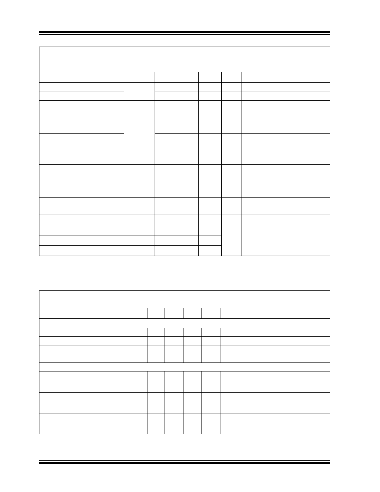
TX Output HD2 & Timing Characteristics
Second Harmonic Distortion
HD2
—
-44
-40
dB
V
PP0
/V
NN0
= ±70V launched in
100 µs apart, with load of
220 pF//1k (Second Harmonic
Distortion).
HD2, single-cycle inverting
5.0 MHz
Note 1
All these tr,tf,td values, at
V
PP0,1
/V
NN0,1
= ±70V, 220 pF//1k
Note 1
Output Rise Time from 0V to V
PP0
t
r1
—
10
12
ns
Output Fall Time from 0V to V
NN0
t
f1
—
10
12
Output Rise Time from V
NN0
to V
PP0
t
r2
—
17
19
Output Fall Time from V
PP0
to V
NN0
t
f2
—
17
19
Output Rise Time from V
NN0
to 0V
t
r3
—
10
13.5
Output Fall Time from V
PP0
to 0V
t
f3
—
10
13.5
Propagation Delay Rise Time 1
t
dr1
—
16
18
ns
Propagation Delay Fall Time 1
t
df1
—
16
18
Propagation Delay Rise Time 2
t
dr2
—
17.5
19
Propagation Delay Fall Time 2
t
df2
—
17.5
19
Propagation Delay Rise Time 3
t
dr3
—
14
16
Propagation Delay Fall Time 3
t
df3
—
14
16
Output Rise Time from 0V to
V
PP1
t
r4
—
15
17
ns
All these tr,tf,td values at
V
PP0,1
/V
NN0,1
=
±70V,
220 pF//1k
Note 1
Output Fall Time from 0V to
V
NN1
t
f4
—
15
17
Output Rise Time from V
NN1
to
V
PP1
t
r5
—
24
27
Output Fall Time from V
PP1
to
V
NN1
t
f5
—
24
27
Output Rise Time from V
NN1
to
0V
t
r6
—
10
13
Output Fall Time from V
PP1
to 0V
t
f6
—
10
13
Propagation Delay Rise Time 4
t
dr4
—
15
17
ns
Propagation Delay Fall Time 4
t
df4
—
15
17
Propagation Delay Rise Time 5
t
dr5
—
16
18
Propagation Delay Fall Time 5
t
df5
—
16
18
Propagation Delay Rise Time 6
t
dr6
—
15
17
Propagation Delay Fall Time 6
t
df6
—
15
17
Delay Time Matching with
SEL = L
∆t
d1
—
1.5
2.0
ns
P to N, ch.-to-ch. matching in IC,
typ. at V
PP0,1
/V
NN0,1,2
= ±70V,
220 pF//1k
,
Note 1
Delay Time Matching with
SEL = H
∆t
d2
—
1.5
2.0
ns
ELECTRICAL CHARACTERISTICS (CONTINUED)
Electrical specifications:
V
LL
= +2.5V, V
DD
= +5.0V, V
PP0,1
= +80V, V
NN0,1,2
= -80V, V
GP
= +10V, V
GN
= -10V,
V
SUB
= 0V, PWS = OEN = REN = 1, T
A
= 25°C, unless otherwise specified. Parameters in Bold apply over the
operating temperature range of T
A
= T
J
= 0 to +85°C.
Parameter
Sym.
Min.
Typ.
Max.
Unit
Conditions
Note 1:
Characterized only; not 100% tested in production.
2:
Design guidance only.
HV7321
DS20005639A-page 10
2016 Microchip Technology Inc.
TRSW Switch On Delay Time
t
TRSW
130
180
230
ns
From POS = 0 & NEG = 0,
Note 1
TRSW Switch Off Delay Time
8
12
16
ns
From POS = 1 or NEG = 1,
Note 1
RTZSW Switch On Delay Time
t
RTZSW
130
180
240
ns
From POS = 0 & NEG = 0,
Note 1
RTZSW Switch Off Delay Time
11
21
31
ns
From POS = 1 or NEG = 1,
Note 1
RXDMP Damp Switch On Delay
Time
t
RXDMP
3
10
15
ns
From POS = 1 or NEG = 1,
Note 1
RXDMP Damp Switch Off Delay
Time
0.55
1.4
2.35
us
From POS = 0 & NEG = 0,
Note 1
PWS = 0 to 1 Mode Change
Time
t
MC
—
220
—
ns
Note 2
Output Max. Frequency Range
f
OUT
—
20
—
MHz
100Ω resistor load,
Note 2
Re-Timing Clock Frequency
f
CLK
10
—
220
MHz
Note 2
Re-Timing Clock Rise & Fall
Times
t
RC
,t
FC
—
0.5
5.0
ns
Note 2
Set-Up Time, POS/NEG to CLK
t
su
2.0
—
—
ns
Note 2
Hold Time, CLK to POS/NEG
t
H
1.0
—
—
ns
Note 2
Clock Time Low
(
2
)
t
CLK_LO
2.0
—
100
ns
CLK input must be activated
before POS and NEG inputs are
high. CLK input must be deacti-
vated after POS and NEG inputs
are low.
Clock Time High
(
2
)
t
CLK_HI
2.0
—
100
Clock Recognition Time
(
1
)
t
CLK_REC
—
2.0
—
Clock Release Time
(
1
)
t
CLK_RLS
150
330
500
TEMPERATURE CHARACTERISTICS
Unless otherwise indicated, all parameters apply with V
LL
= +2.5V, V
DD
= +5.0V, V
PP0,1
= +80V, V
NN0,1,2
= -80V,
V
GP
= +10V, V
GN
= -10V, V
SUB
= 0V, OEN = REN = 1
Parameters
Sym. Min. Typ.
Max.
Units
Conditions
Temperature Ranges
Operating Ambient Temperature Range
T
OA
0
—
+85
°C
Storage Temperature Range
T
ST
-55
—
+150
°C
Maximum Junction Temperature
T
J
—
—
+130
°C
Total Power Dissipation
PD
—
3.0
—
W
Thermal Package Resistances (64LD 9 mm x 9 mm VQFN)
Junction-to-Ambient Thermal Resistance
JA
—
16.3
—
°C/W
JEDEC (2S2P) 4L PCB
114.3 mm x 76.2 mm x1.6 mm
T
A
= 85°C
Junction-to-Board Thermal Resistance
JB
—
2.55
—
°C/W
JEDEC (2S2P) 4L PCB
114.3 mm x 76.2 mm x1.6 mm
T
A
= 85°C
Junction-to-Case Top Thermal Resistance
JC
—
0.2
—
°C/W
JEDEC (2S2P) 4L PCB
114.3 mm x 76.2 mm x1.6 mm
T
A
= 85°C
ELECTRICAL CHARACTERISTICS (CONTINUED)
Electrical specifications:
V
LL
= +2.5V, V
DD
= +5.0V, V
PP0,1
= +80V, V
NN0,1,2
= -80V, V
GP
= +10V, V
GN
= -10V,
V
SUB
= 0V, PWS = OEN = REN = 1, T
A
= 25°C, unless otherwise specified. Parameters in Bold apply over the
operating temperature range of T
A
= T
J
= 0 to +85°C.
Parameter
Sym.
Min.
Typ.
Max.
Unit
Conditions
Note 1:
Characterized only; not 100% tested in production.
2:
Design guidance only.