
© 2007 Microchip Technology Inc.
DS22022B-page 1
MCP1403/4/5
Features
• High Peak Output Current: 4.5A (typ.)
• Low Shoot-Through/Cross-Conduction Current in
Output Stage
• Wide Input Supply Voltage Operating Range:
- 4.5V to 18V
• High Capacitive Load Drive Capability:
- 2200 pF in 15 ns
- 5600 pF in 34 ns
• Short Delay Times: 40 ns (typ.)
• Low Supply Current:
- With Logic ‘1’ Input – 1.0 mA (typ.)
- With Logic ‘0’ Input – 150 µA (typ.)
• Latch-Up Protected: Will Withstand 1.5A Reverse
Current
• Logic Input Will Withstand Negative Swing
Up To 5V
• Packages: 8-Pin SOIC, PDIP, 8-Pin 6x5 DFN,
and 16-Pin SOIC
Applications
• Switch Mode Power Supplies
• Pulse Transformer Drive
• Line Drivers
• Motor and Solenoid Drive
General Description
The MCP1403/4/5 are a family of dual-inverting, dual-
non-inverting, or complimentary output drivers. They
can delivery high peak currents of 4.5A typically into
capacitive loads. These devices also feature low shoot-
through current, matched rise/fall times and
propagation delays.
The MCP1403/4/5 drivers operate from a 4.5V to 18V
single power supply and can easily charge and
discharge 2200 pF gate capacitance in under 15 ns
(typ). They provide low enough impedances in both the
on and off states to ensure the MOSFETs intended
state will not be affected, even by large transients. The
input to the MCP1403/4/5 may be driven directly from
either TTL or CMOS (3V to 18V).
The MCP1403/4/5 dual-output 4.5A driver family is
offered in both surface-mount and pin-through-hole
packages with a -40
o
C to +125
o
C temperature rating.
The low thermal resistance of the thermally enhanced
DFN package allows for greater power dissipation
capability for driving heavier capacitive or resistive
loads.
These devices are highly latch-up resistant under any
conditions within their power and voltage ratings. They
are not subject to damage when up to 5V of noise
spiking (of either polarity) occurs on the ground pin. All
terminals are fully protect against Electrostatic
Discharge (ESD) up to 4 kV.
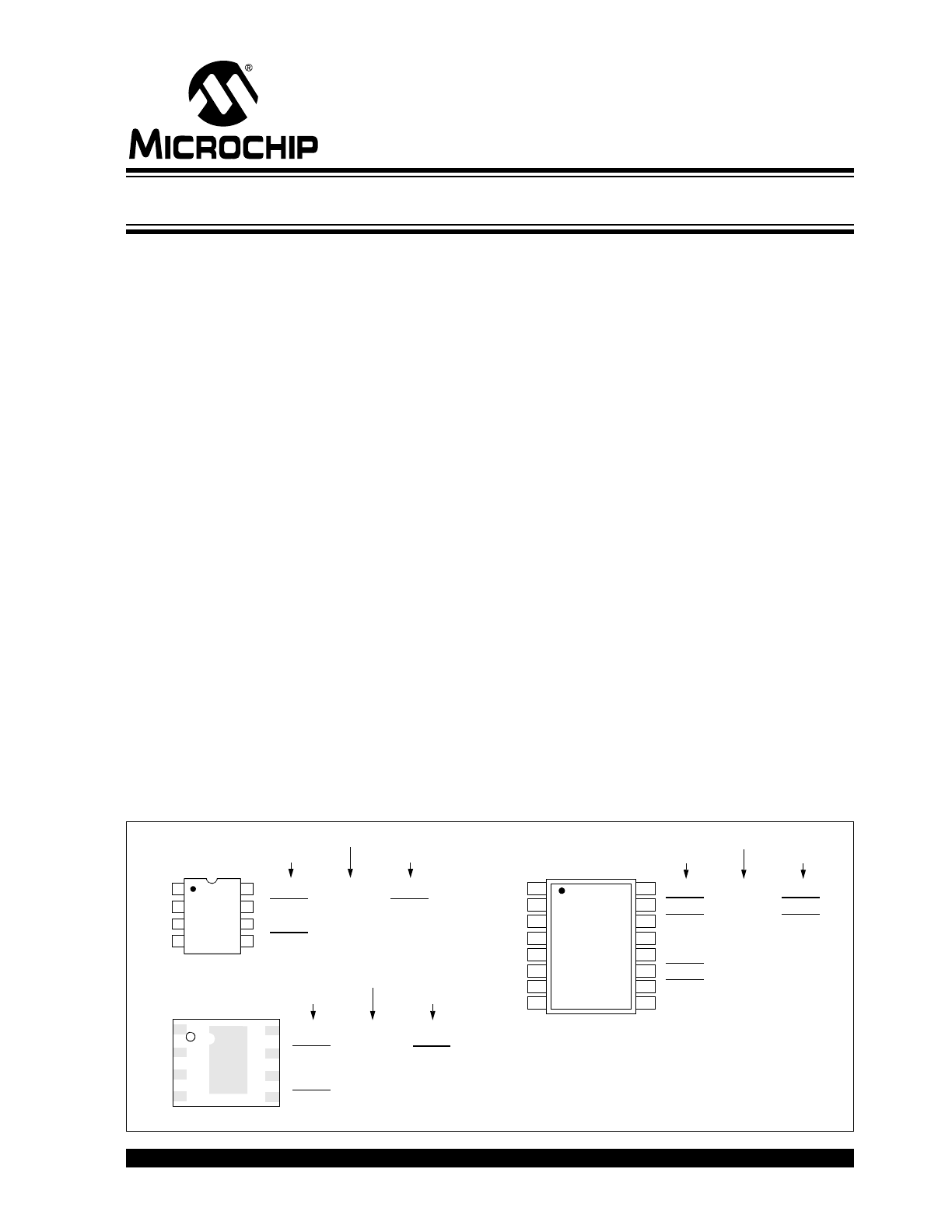
Package Types
8-Pin DFN
(2)
NC
IN A
GND
IN B
2
3
4
5
6
7
8
1
8-Pin
1
2
3
4
NC
5
6
7
8
OUT A
OUT B
NC
IN A
GND
IN B
V
DD
Note 1: Duplicate pins must both be connected for
proper operation.
2: Exposed pad of the DFN package is electrically
isolated.
MCP1403
MCP1404
NC
OUT A
OUT B
V
DD
MCP1405
NC
OUT A
OUT B
V
DD
1
2
3
4
5
6
7
8
16
13
12
11
10
9
NC
IN A
NC
GND
GND
NC
IN B
NC
NC
OUT A
V
DD
V
DD
OUT B
OUT B
NC
OUT A
15
14
16-Pin SOIC
NC
OUT A
V
DD
V
DD
OUT B
OUT B
NC
OUT A
OUT A
V
DD
V
DD
OUT B
OUT B
NC
OUT A
MCP1403
MCP1404
MCP1405
NC
NC
OUT A
OUT B
V
DD
MCP1403
MCP1404
NC
OUT A
OUT B
V
DD
MCP1405
NC
OUT A
OUT B
V
DD
PDIP/SOIC
4.5A Dual High-Speed Power MOSFET Drivers
MCP1403/4/5
DS22022B-page 2
© 2007 Microchip Technology Inc.
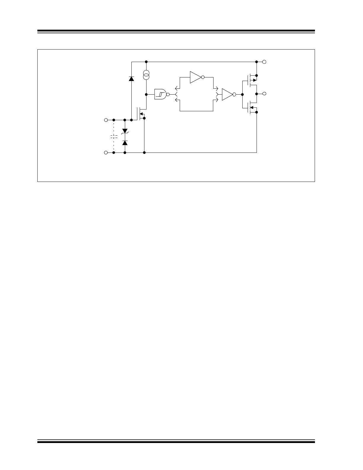
Functional Block Diagram
(1)
Effective
Input C = 20 pF
MCP1403 Dual Inverting
MCP1404 Dual Non-inverting
Input
GND
V
DD
300 mV
4.7V
Inverting
Non-inverting
Note 1: Unused inputs should be grounded.
730 µA
Output
(Each Input)
MCP1405 Inverting / Non-inverting
© 2007 Microchip Technology Inc.
DS22022B-page 3
MCP1403/4/5
1.0
ELECTRICAL
CHARACTERISTICS
Absolute Maximum Ratings †
Supply Voltage ................................................................+20V
Input Voltage ...............................(V
DD
+ 0.3V) to (GND – 5V)
Input Current (V
IN
>V
DD
)................................................50 mA
† Notice: Stresses above those listed under "Maximum
Ratings" may cause permanent damage to the device. This is
a stress rating only and functional operation of the device at
those or any other conditions above those indicated in the
operational sections of this specification is not intended.
Exposure to maximum rating conditions for extended periods
may affect device reliability.
DC CHARACTERISTICS (NOTE 2)
Electrical Specifications: Unless otherwise indicated, T
A
= +25°C, with 4.5V
≤ V
DD
≤ 18V.
Parameters
Sym
Min
Typ
Max
Units
Conditions
Input
Logic ‘1’, High Input Voltage
V
IH
2.4
1.5
—
V
Logic ‘0’, Low Input Voltage
V
IL
—
1.3
0.8
V
Input Current
I
IN
–1
—
1
µA
0V
≤ V
IN
≤ V
DD
Input Voltage
V
IN
-5
—
V
DD
+0.3
V
Output
High Output Voltage
V
OH
V
DD
– 0.025
—
—
V
DC Test
Low Output Voltage
V
OL
—
—
0.025
V
DC Test
Output Resistance, High
R
OH
—
2.2
3.0
Ω
I
OUT
= 10 mA, V
DD
= 18V
Output Resistance, Low
R
OL
—
2.8
3.5
Ω
I
OUT
= 10 mA, V
DD
= 18V
Peak Output Current
I
PK
—
4.5
—
A
V
DD
= 18V (Note 2)
Latch-Up Protection With-
stand Reverse Current
I
REV
—
>1.5
—
A
Duty cycle
≤ 2%, t ≤ 300 µsec.
Switching Time (Note 1)
Rise Time
t
R
—
15
28
ns
Figure 4-1
,
Figure 4-2
C
L
= 2200 pF
Fall Time
t
F
—
18
28
ns
Figure 4-1
,
Figure 4-2
C
L
= 2200 pF
Delay Time
t
D1
—
40
48
ns
Figure 4-1
,
Figure 4-2
Delay Time
t
D2
—
40
48
ns
Figure 4-1
,
Figure 4-2
Power Supply
Supply Voltage
V
DD
4.5
—
18.0
V
Power Supply Current
I
S
—
1.0
2.0
mA
V
IN
= 3V (Both Inputs)
I
S
—
0.15
0.25
mA
V
IN
= 0V (Both Inputs)
Note 1: Switching times ensured by design.
2: Tested during characterization, not production tested.
MCP1403/4/5
DS22022B-page 4
© 2007 Microchip Technology Inc.
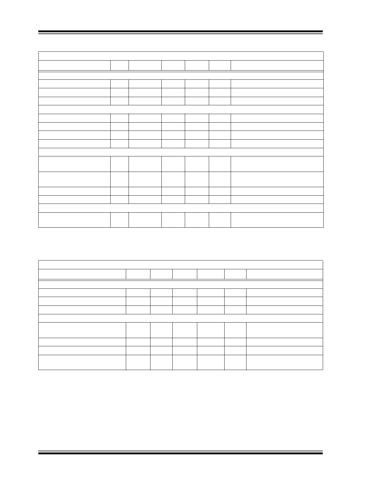
DC CHARACTERISTICS (OVER OPERATING TEMPERATURE RANGE)
TEMPERATURE CHARACTERISTICS
Electrical Specifications: Unless otherwise indicated, operating temperature range with 4.5V
≤ V
DD
≤ 18V.
Parameters
Sym
Min
Typ
Max
Units
Conditions
Input
Logic ‘1’, High Input Voltage
V
IH
2.4
—
—
V
Logic ‘0’, Low Input Voltage
V
IL
—
—
0.8
V
Input Current
I
IN
–10
—
+10
µA
0V
≤ V
IN
≤ V
DD
Output
High Output Voltage
V
OH
V
DD
– 0.025
—
—
V
DC TEST
Low Output Voltage
V
OL
—
—
0.025
V
DC TEST
Output Resistance, High
R
OH
—
3.1
6.0
Ω
I
OUT
= 10 mA, V
DD
= 18V
Output Resistance, Low
R
OL
—
3.7
7
Ω
I
OUT
= 10 mA, V
DD
= 18V
Switching Time (Note 1)
Rise Time
t
R
—
25
40
ns
Figure 4-1
,
Figure 4-2
C
L
= 2200 pF
Fall Time
t
F
—
25
40
ns
Figure 4-1
,
Figure 4-2
C
L
= 2200 pF
Delay Time
t
D1
—
50
65
ns
Figure 4-1
,
Figure 4-2
Delay Time
t
D2
—
50
65
ns
Figure 4-1
,
Figure 4-2
Power Supply
Power Supply Current
I
S
—
—
2.0
0.2
3.0
0.3
mA
V
IN
= 3V (Both Inputs)
V
IN
= 0V (Both Inputs)
Note 1: Switching times ensured by design.
2: Tested during characterization, not production tested.
Electrical Specifications: Unless otherwise noted, all parameters apply with 4.5V
≤ V
DD
≤ 18V.
Parameters
Sym
Min
Typ
Max
Units
Conditions
Temperature Ranges
Specified Temperature Range
T
A
–40
—
+125
°C
Maximum Junction Temperature
T
J
—
—
+150
°C
Storage Temperature Range
T
A
–65
—
+150
°C
Package Thermal Resistances
Thermal Resistance, 8L-6x5 DFN
θ
JA
—
33.2
—
°C/W
Typical four-layer board with
vias to ground plane
Thermal Resistance, 8L-PDIP
θ
JA
—
125
—
°C/W
Thermal Resistance, 8L-SOIC
θ
JA
—
155
—
°C/W
Thermal Resistance, 16L-SOIC
θ
JA
—
155
—
°C/W
4-Layer JC51-7 Standard
Board, Natural Convection
© 2007 Microchip Technology Inc.
DS22022B-page 5
MCP1403/4/5
2.0
TYPICAL PERFORMANCE CURVES
Note: Unless otherwise indicated, T
A
= +25°C with 4.5V
≤ V
DD
≤ 18V.
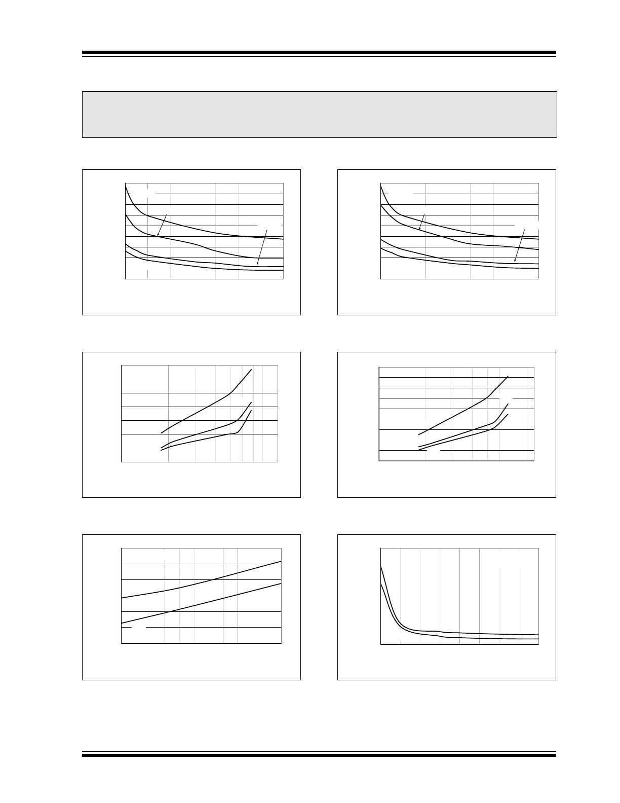
FIGURE 2-1:
Rise Time vs. Supply
Voltage.
FIGURE 2-2:
Rise Time vs. Capacitive
Load.
FIGURE 2-3:
Rise and Fall Times vs.
Temperature.
FIGURE 2-4:
Fall Time vs. Supply
Voltage.
FIGURE 2-5:
Fall Time vs. Capacitive
Load.
FIGURE 2-6:
Propagation Delay vs. Input
Amplitude.
Note:
The graphs and tables provided following this note are a statistical summary based on a limited number of
samples and are provided for informational purposes only. The performance characteristics listed herein
are not tested or guaranteed. In some graphs or tables, the data presented may be outside the specified
operating range (e.g., outside specified power supply range) and therefore outside the warranted range.
10
20
30
40
50
60
70
80
90
100
4
6
8
10
12
14
16
18
Supply Voltage (V)
Ri
se Ti
me (
n
s
)
6800 pF
4700 pF
2200 pF
1800 pF
10
20
30
40
50
60
70
80
1000
10000
Capacitive Load (pF)
R
ise
T
im
e (
n
s)
5V
18V
12V
12
14
16
18
20
22
24
-40 -25 -10 5
20 35 50 65 80 95 110 125
Temperature (
o
C)
Time (ns
)
t
FALL
t
RISE
C
LOAD
= 1800 pF
10
20
30
40
50
60
70
80
90
100
4
6
8
10
12
14
16
18
Supply Voltage (V)
F
all
T
im
e (n
s)
6800 pF
4700 pF
2200 pF
1800 pF
10
20
30
40
50
60
70
80
90
100
1000
10000
Capacitive Load (pF)
Fa
ll Time
(
n
s)
5V
18V
12V
35
60
85
110
135
160
2
3
4
5
6
7
8
9
10
Input Amplitude (V)
Pr
op
ag
at
io
n
De
lay
(
n
s)
t
D1
t
D2
V
DD
= 12V
C
LOAD
= 1800 pF
MCP1403/4/5
DS22022B-page 6
© 2007 Microchip Technology Inc.
Typical Performance Curves (Continued)
Note: Unless otherwise indicated, T
A
= +25°C with 4.5V
≤ V
DD
≤ 18V.
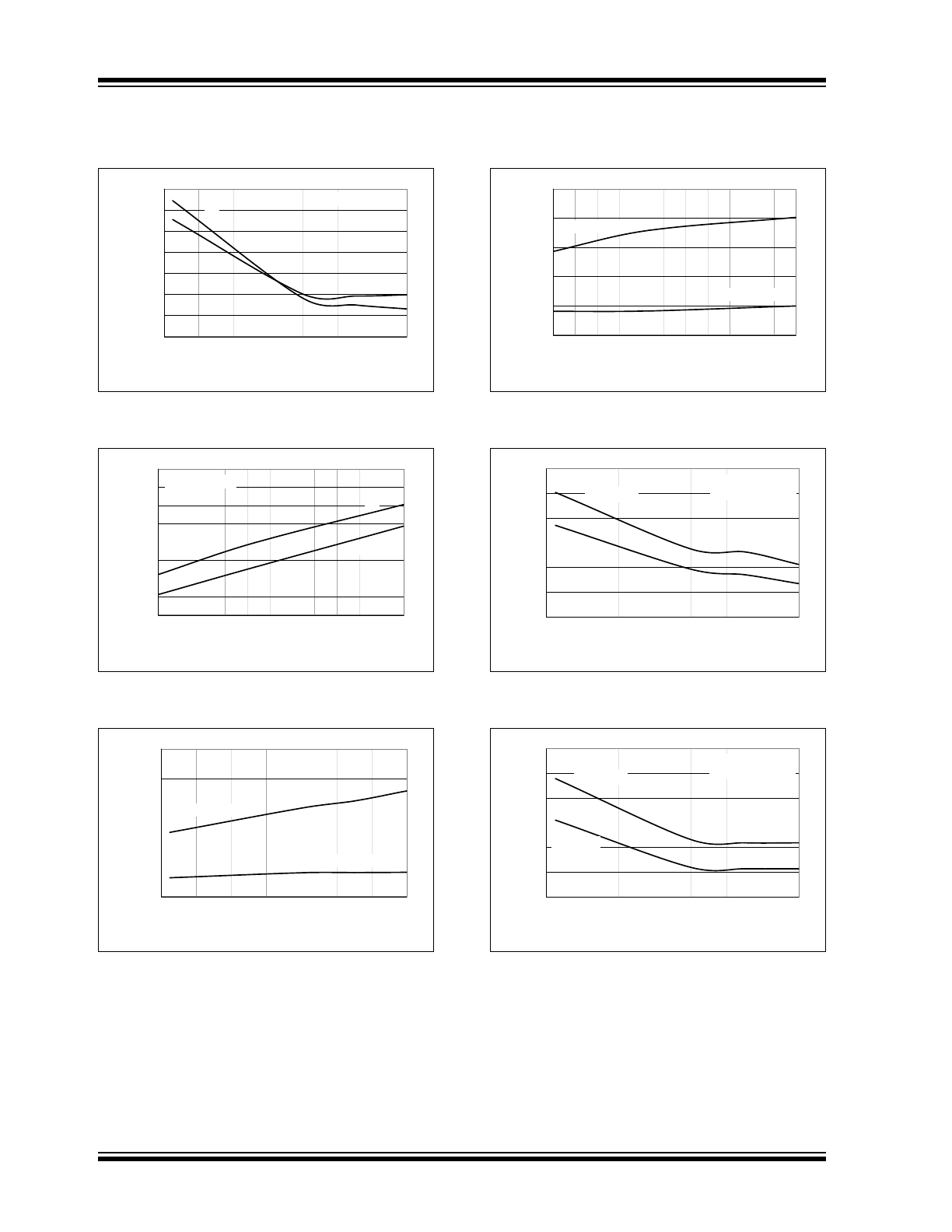
FIGURE 2-7:
Propagation Delay Time vs.
Supply Voltage.
FIGURE 2-8:
Propagation Delay Time vs.
Temperature.
FIGURE 2-9:
Quiescent Current vs.
Supply Voltage.
FIGURE 2-10:
Quiescent Current vs.
Temperature.
FIGURE 2-11:
Output Resistance (Output
High) vs. Supply Voltage.
FIGURE 2-12:
Output Resistance (Output
Low) vs. Temperature.
30
40
50
60
70
80
90
100
4
6
8
10
12
14
16
18
Supply Voltage (V)
P
rop
ag
ati
o
n
D
e
la
y
(ns
)
t
D1
t
D2
C
LOAD
= 1800 pF
30
35
40
45
50
55
60
65
70
-40 -25 -10 5
20 35 50 65 80 95 110 125
Temperature (
o
C)
Pr
op
ag
at
io
n
D
el
ay
(n
s
)
t
D1
t
D2
C
LOAD
= 1800 pF
0
0.1
0.2
0.3
0.4
0.5
4
6
8
10
12
14
16
18
Supply Voltage (V)
Qu
ie
sc
en
t Cu
rre
n
t (mA
)
Both Inputs = 1
Both Inputs = 0
0
0.1
0.2
0.3
0.4
0.5
-40 -25 -10 5
20 35 50 65 80 95 110 125
Temperature (
o
C)
Qu
iesc
en
t Cu
rre
nt
(
m
A)
Both Inputs = 1
Both Inputs = 0
1
2
3
4
5
6
7
4
6
8
10
12
14
16
18
Supply Voltage (V)
R
OUT-HI
(
::
)
T
J
= +150
o
C
T
J
= +25
o
C
V
IN
= 5V (MCP1404)
V
IN
= 0V (MCP1403)
2
3
4
5
6
7
8
4
6
8
10
12
14
16
18
Supply Voltage (V)
R
OUT-LO
(
::
)
T
J
= +150
o
C
T
J
= +25
o
C
V
IN
= 0V (MCP1404)
V
IN
= 5V (MCP1403)
© 2007 Microchip Technology Inc.
DS22022B-page 7
MCP1403/4/5
Typical Performance Curves (Continued)
Note: Unless otherwise indicated, T
A
= +25°C with 4.5V
≤ V
DD
≤ 18V.
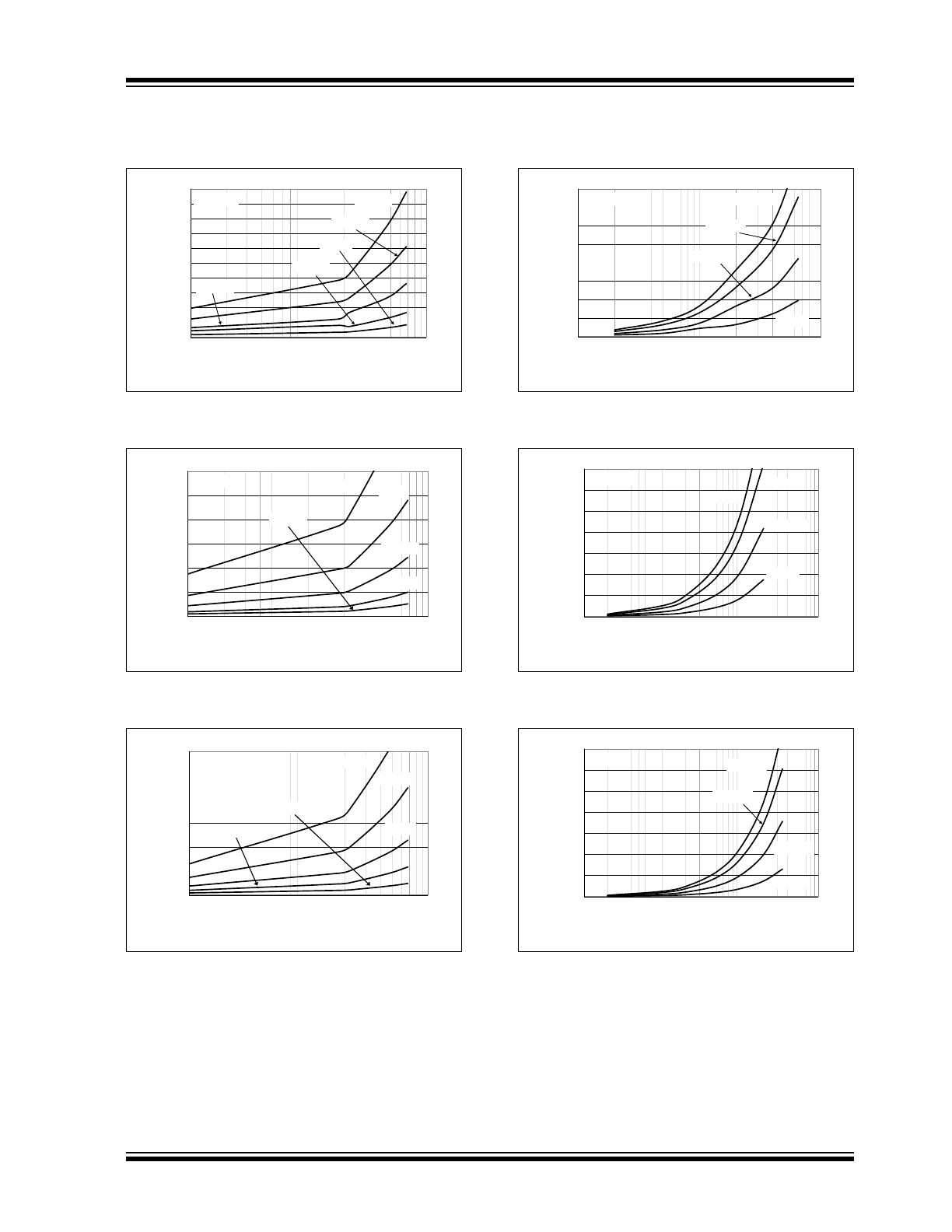
FIGURE 2-13:
Supply Current vs.
Capacitive Load.
FIGURE 2-14:
Supply Current vs.
Capacitive Load.
FIGURE 2-15:
Supply Current vs.
Capacitive Load.
FIGURE 2-16:
Supply Current vs.
Frequency.
FIGURE 2-17:
Supply Current vs.
Frequency.
FIGURE 2-18:
Supply Current vs.
Frequency.
0
10
20
30
40
50
60
70
80
90
100
100
1000
10000
Capacitive Load (pF)
Su
pply Cu
rr
en
t
(mA
)
650 kHz
V
DD
= 18V
50 kHz
100 kHz
200 kHz
400 kHz
0
20
40
60
80
100
120
100
1000
10000
Capacitive Load (pF)
Supply Current (mA)
2 MHz
V
DD
= 12V
500 kHz
200 kHz
100 kHz
1 MHz
0
20
40
60
80
100
120
100
1000
10000
Capacitive Load (pF)
Su
ppl
y Cu
rr
e
n
t (m
A
)
3.5 MHz
V
DD
= 6V
1 MHz
500 kHz
200 kHz
2 MHz
0
10
20
30
40
50
60
70
80
10
100
1000
Frequency (kHz)
S
u
ppl
y Cu
rre
n
t (mA
)
V
DD
= 18V
6,800 pF
100 pF
2,200 pF
4,700 pF
0
20
40
60
80
100
120
140
10
100
1000
10000
Frequency (kHz)
S
u
ppl
y Cu
rre
n
t (mA
)
V
DD
= 12V
6,800 pF
100 pF
2,200 pF
4,700 pF
0
20
40
60
80
100
120
140
10
100
1000
10000
Frequency (kHz)
Supp
ly
Curre
nt (mA)
V
DD
= 6V
6,800 pF
100 pF
2,200 pF
4,700 pF
MCP1403/4/5
DS22022B-page 8
© 2007 Microchip Technology Inc.
Typical Performance Curves (Continued)
Note: Unless otherwise indicated, T
A
= +25°C with 4.5V
≤ V
DD
≤ 18V.
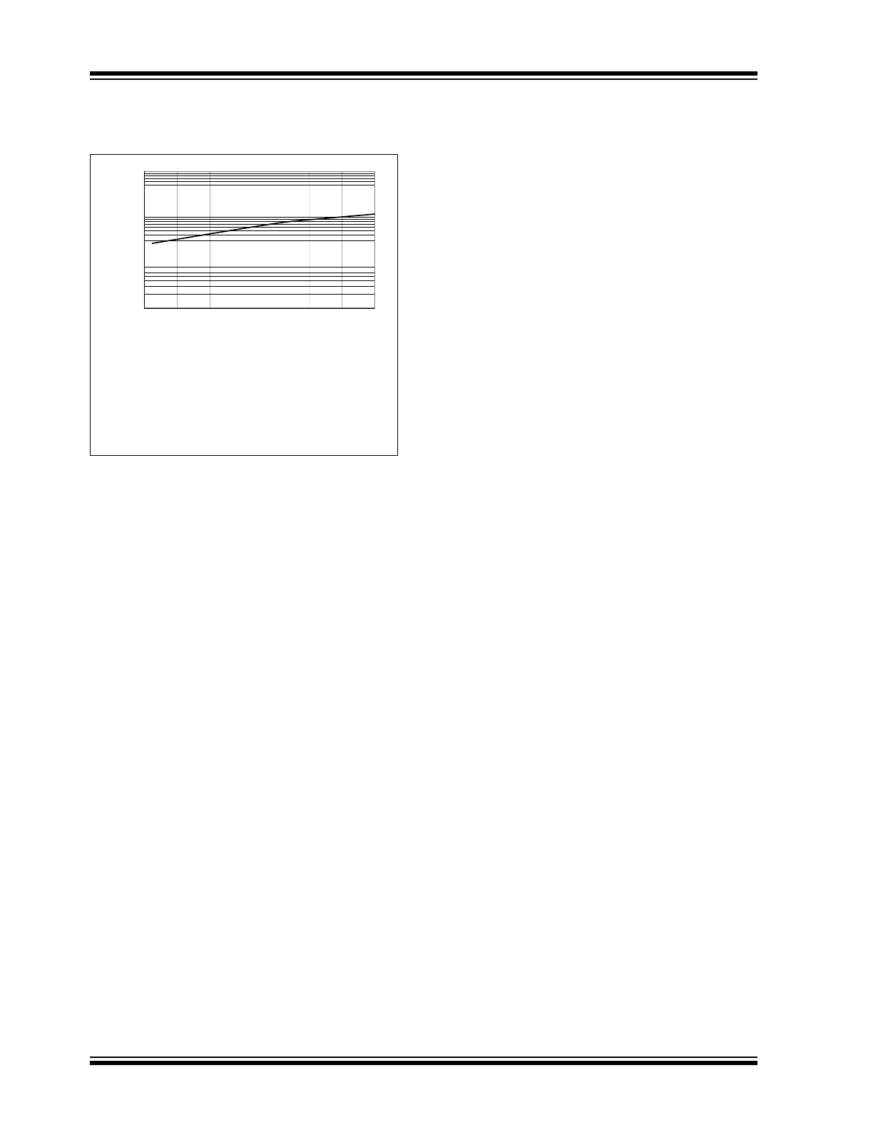
FIGURE 2-19:
Crossover Energy vs.
Supply Voltage.
1.00E-09
1.00E-08
1.00E-07
1.00E-06
4
6
8
10
12
14
16
18
Supply Voltage (V)
C
ros
sov
er En
erg
y (A*
sec)
10
-6
10
-7
10
-8
10
-9
Note:
The values on this graph represent the
loss seen by both drivers in a package
during one complete cycle. For a sin-
gle driver, divide the stated value by 2.
For a single transition of a single driver
divide the stated value by 4.
© 2007 Microchip Technology Inc.
DS22022B-page 9
MCP1403/4/5
3.0
PIN DESCRIPTIONS
The descriptions of the pins are listed in
Table 3-1
.
TABLE 3-1:
PIN FUNCTION TABLE
(1)
3.1
Supply Input (V
DD
)
V
DD
is the bias supply input for the MOSFET driver and
has a voltage range of 4.5V to 18V. This input must be
decoupled to ground with a local capacitor. This bypass
capacitor provides a localized low-impedance path for
the peak currents that are to be provided to the load.
3.2
Control Inputs A and B
The MOSFET driver input is a high-impedance, TTL/
CMOS-compatible input. The input also has hysteresis
between the high and low input levels, allowing them to
be driven from slow rising and falling signals, and to
provide noise immunity.
3.3
Ground (GND)
Ground is the device return pin. The ground pin should
have a low impedance connection to the bias supply
source return. High peak currents will flow out the
ground pin when the capacitive load is being
discharged.
3.4
Outputs A and B
Outputs A and B are CMOS push-pull output that is
capable of sourcing and sinking 4.5A of peak current
(V
DD
= 18V). The low output impedance ensures the
gate of the external MOSFET will stay in the intended
state even during large transients. These output also
has a reverse current latch-up rating of 1.5A.
3.5
Exposed Metal Pad
The exposed metal pad of the DFN package is not
internally connected to any potential. Therefore, this
pad can be connected to a ground plane or other
copper plane on a printed circuit board to aid in heat
removal from the package.
8-Pin
PDIP
SOIC
8-Pin
DFN
16-Pin
SOIC
Symbol
Description
1
1
1
NC
No Connection
2
2
2
IN A
Control Input for Output A
—
—
3
NC
No Connection
3
3
4
GND
Ground
—
—
5
GND
Ground
—
—
6
NC
No Connection
4
4
7
IN B
Control Input for Output B
—
—
8
NC
No Connection
—
—
9
NC
No Connection
5
5
10
OUT B
Output B
—
—
11
OUT B
Output B
6
6
12
V
DD
Supply Input
—
—
13
V
DD
Supply Input
7
7
14
OUT A
Output A
—
—
15
OUT A
Output A
8
8
16
NC
No Connection
—
PAD
—
NC
Exposed Metal Pad
Note 1: Duplicate pins must be connected for proper operation.
MCP1403/4/5
DS22022B-page 10
© 2007 Microchip Technology Inc.
4.0
APPLICATION INFORMATION
4.1
General Information
MOSFET drivers are high-speed, high current devices
which are intended to source/sink high peak currents to
charge/discharge the gate capacitance of external
MOSFETs or IGBTs. In high frequency switching
power supplies, the PWM controller may not have the
drive capability to directly drive the power MOSFET. A
MOSFET driver like the MCP1403/4/5 family can be
used to provide additional source/sink current
capability.
4.2
MOSFET Driver Timing
The ability of a MOSFET driver to transition from a fully
off state to a fully on state are characterized by the driv-
ers rise time (t
R
), fall time (t
F
), and propagation delays
(t
D1
and t
D2
). The MCP1403/4/5 family of drivers can
typically charge and discharge a 2200 pF load capaci-
tance in 15 ns along with a typical matched propaga-
tion delay of 40 ns.
Figure 4-1
and
Figure 4-2
show the
test circuit and timing waveform used to verify the
MCP1403/4/5 timing.
FIGURE 4-1:
Inverting Driver Timing
Waveform.
FIGURE 4-2:
Non-Inverting Driver Timing
Waveform.
4.3
Decoupling Capacitors
Careful layout and decoupling capacitors are highly
recommended when using MOSFET drivers. Large
currents are required to charge and discharge
capacitive loads quickly. For example, 2.5A are needed
to charge a 2200 pF load with 18V in 16 ns.
To operate the MOSFET driver over a wide frequency
range with low supply impedance a ceramic and low
ESR film capacitor are recommended to be placed in
parallel between the driver V
DD
and GND. A 1.0 µF low
ESR film capacitor and a 0.1 µF ceramic capacitor
placed between
V
DD
and GND pins
should be used.
These capacitors should be placed close to the driver
to minimized circuit board parasitics and provide a local
source for the required current.
4.4
PCB Layout Considerations
Proper PCB layout is important in a high current, fast
switching circuit to provide proper device operation and
robustness of design. PCB trace loop area and
inductance should be minimized by the use of ground
planes or trace under MOSFET gate drive signals,
separate analog and power grounds, and local driver
decoupling.
0.1 µF
+5V
10%
90%
10%
90%
10%
90%
18V
1 µF
0V
0V
MCP1403
C
L
= 2200 pF
Input
Input
Output
t
D1
t
F
t
D2
Output
t
R
V
DD
= 18V
Ceramic
Input
(1/2 MCP1405)
90%
Input
t
D1
t
F
t
D2
Output
t
R
10%
10%
10%
+5V
18V
0V
0V
90%
90%
0.1 µF
1 µF
MCP1404
C
L
= 2200 pF
Input
Output
V
DD
= 18V
Ceramic
Input
(1/2 MCP1405)