
2018 Microchip Technology Inc.
DS20005897B-page 1
MIC29302A
Features
• High-Current Capability
• Operating Input Voltage Range: 3V to 16V
• Low Dropout Voltage
• Low Ground Current
• Accurate 1% Tolerance
• Fast Transient Response
• 1.24V to 15V Adjustable Output Voltage
• Packages: TO-263-5L and TO-252-5L
Applications
• Processor Peripheral and I/O Supplies
• High-Efficiency Green Computer Systems
• Automotive Electronics
• High-Efficiency Linear Lower Supplies
• Battery-Powered Equipment
• PC Add-In Cards
• High-Efficiency Post-Regulator for Switching
Supply
General Description
The MIC29302A is a high-current, low-dropout voltage
regulator that uses Microchip's proprietary Super βeta
PNP process with a PNP pass element. The 3A LDO
regulator features 560 mV (full load) dropout voltage
and very low ground current. Designed for high-current
loads, these devices also find applications in lower
current, low-dropout critical systems, where their
dropout voltages and ground current values are
important attributes.
Along with a total accuracy of ±2% (over temperature,
line, and load regulation) the regulator features very
fast transient recovery from input voltage surges and
output load current changes.
The MIC29302A has an adjustable output that can be
set by two external resistors to a voltage between
1.24V and 15V. In addition, the device is fully protected
against overcurrent faults, reversed input polarity,
reversed lead insertion, and overtemperature
operation. A TTL/CMOS logic enable (EN) pin is
available in the MIC29302A to shutdown the regulator.
When not used, the device can be set to continuous
operation by connecting EN to the input (IN). The
MIC29302A is available in the standard and 5-pin
TO-263 and TO-252 packages with an operating
junction temperature range of –40°C to +125°C.
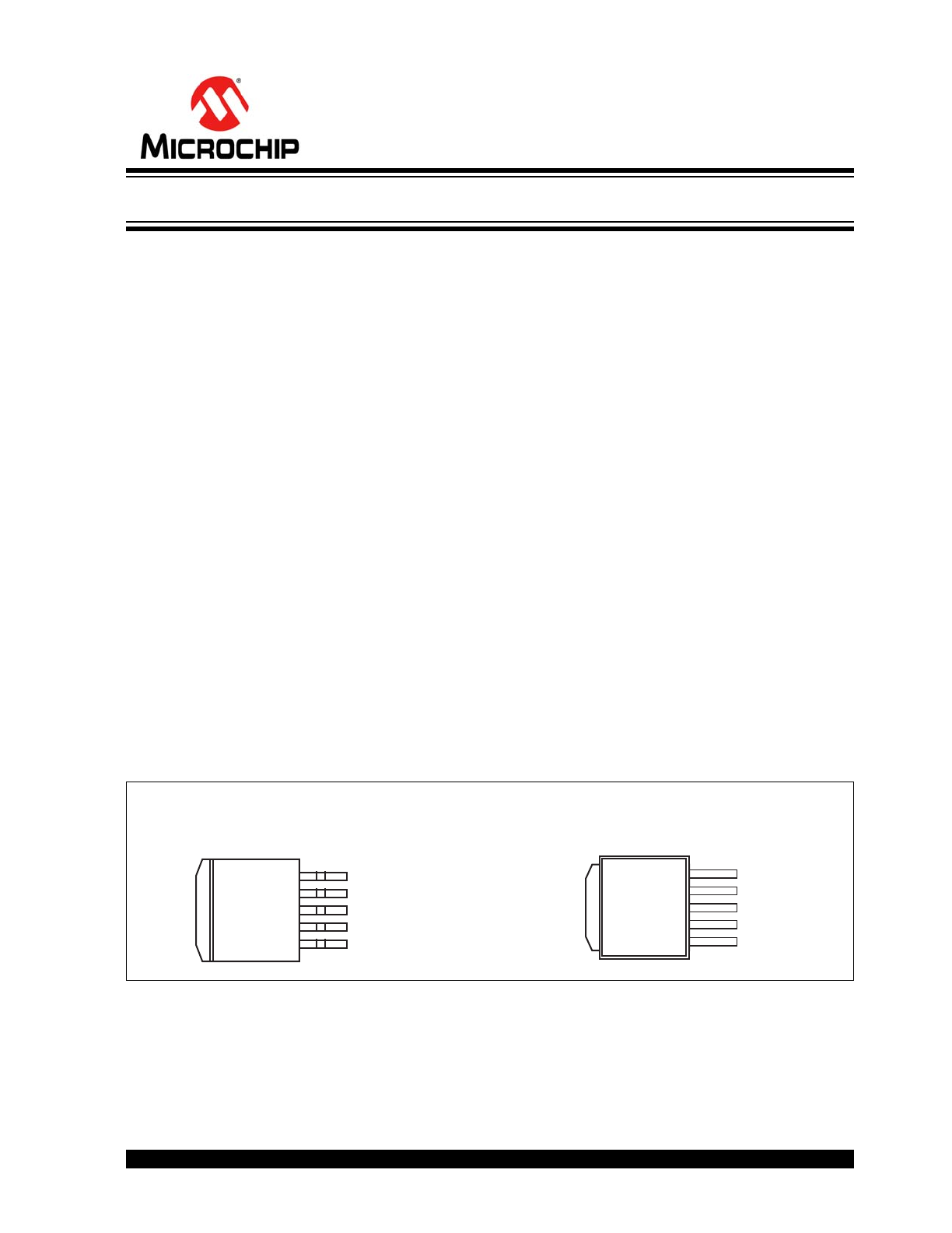
Package Types
MIC29302AWU
5-Lead TO-263 (U)
(D
2
Pak) Adjustable Voltage
MIC29302AWD
5-Lead TO-252 (D)
(D-Pak) Adjustable Voltage
TA
B
4
1
5
2
3
OUT
EN
ADJ
IN
GND
TA
B
5
ADJ
4
OUT
3
GND
2
IN
1
EN
3A Fast Response LDO Regulator
MIC29302A
DS20005897B-page 2
2018 Microchip Technology Inc.
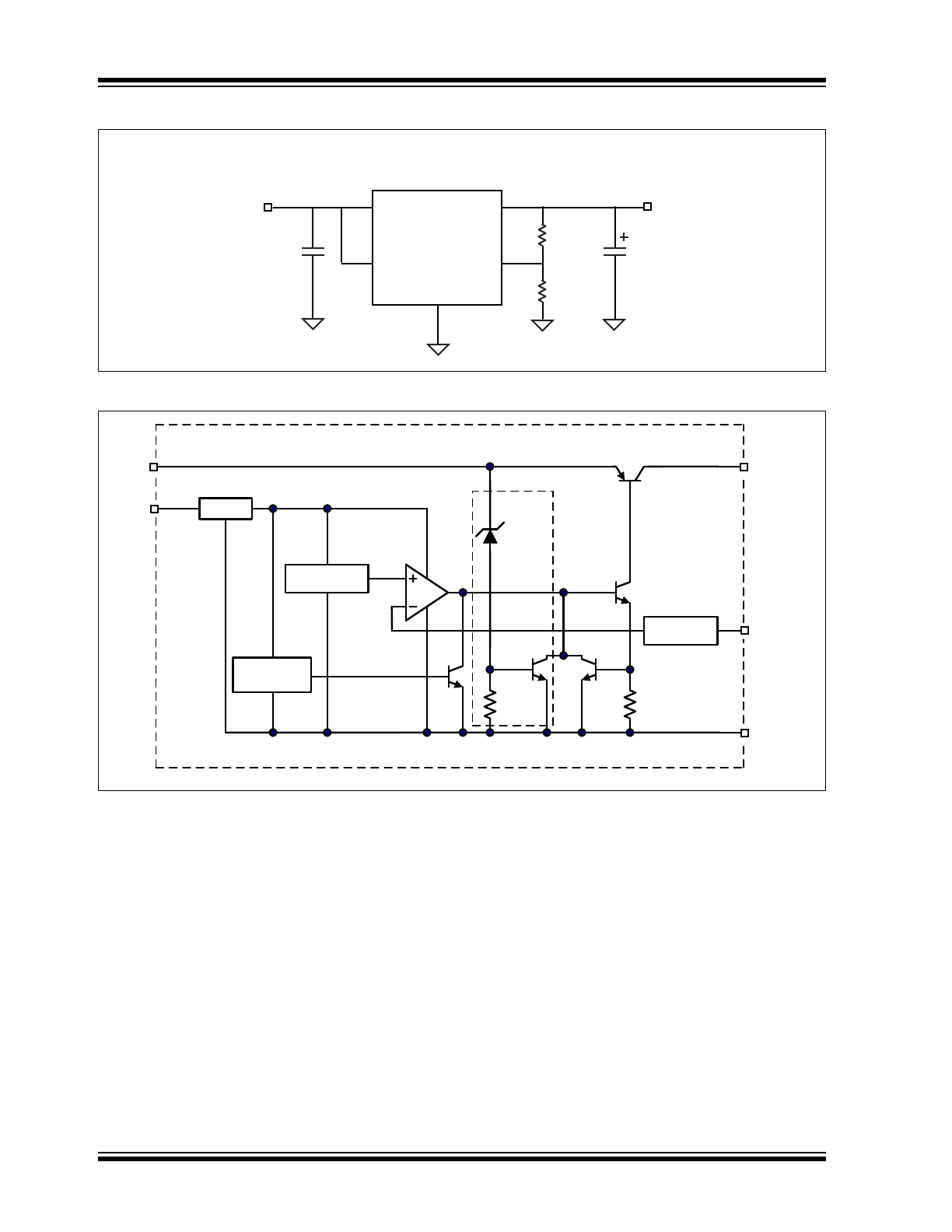
Typical Application Circuit
Functional Block Diagram
MIC29302A
TO-263 or TO-252
3.3V
IN
C
IN
R1
R2
2.5V
OUT
C
L
OUT
IN
EN
ADJ
GND
EN
IN
ADJ
OUT
BIAS
GND
MIC29302A
THERMAL
SHUTDOWN
REFERENCE
ON/OFF
FEEDBACK
O.V.
LIMIT
16V
2018 Microchip Technology Inc.
DS20005897B-page 3
MIC29302A
1.0
ELECTRICAL CHARACTERISTICS
Absolute Maximum Ratings †
Input Supply Voltage (V
IN
) .......................................................................................................................... –20V to +20V
Enable Input Voltage (V
EN
) ............................................................................................................................–0.3V to V
IN
Power Dissipation .................................................................................................................................. Internally Limited
ESD Rating (All Pins) ..............................................................................................................................................
Note 1
Operating Ratings ‡
Operating Input Voltage ................................................................................................................................ +3V to +16V
†
Notice: Stresses above those listed under “Absolute Maximum Ratings” may cause permanent damage to the device.
This is a stress rating only and functional operation of the device at those or any other conditions above those indicated
in the operational sections of this specification is not intended. Exposure to maximum rating conditions for extended
periods may affect device reliability.
‡ Notice:
The device is not guaranteed to function outside its operating ratings.
Note 1:
Devices are ESD sensitive. Handling precautions recommended.
TABLE 1-1:
ELECTRICAL CHARACTERISTICS
Electrical Characteristics:
V
IN
= 4.184V; I
OUT
= 100 mA; T
A
= +25°C, bold values indicate –40°C ≤ T
J
≤ +125°C,
unless noted.
Note 1
Parameter
Symbol
Min.
Typ.
Max.
Units
Conditions
Output Voltage
Output Voltage Accuracy
∆V
OUT
–2
—
2
%
100 mA ≤ I
OUT
≤ 3A, (V
OUT
+ 1V) ≤
V
IN
≤ 16V
Line Regulation
∆V
OUT
/
∆V
IN
—
0.1
0.5
%
I
OUT
= 100 mA, (V
OUT
+ 1V) ≤ V
IN
≤
16V
Load Regulation
∆V
OUT
/
∆I
OUT
—
0.2
1
%
V
IN
= V
OUT
+ 1V, 100 mA ≤ I
OUT
≤
3A
Dropout Voltage (
Note 2
)
V
DO
—
100
200
mV
I
OUT
= 100 mA, V
IN
≥ 3.184V
—
300
—
I
OUT
= 1.5A, V
IN
≥ 3.184V
—
500
—
I
OUT
= 2.75A, V
IN
≥ 3.184V
—
560
800
I
OUT
= 3A, V
IN
≥ 3.4V
Ground Current
Ground Current
I
GND
—
5
20
mA
I
OUT
= 750 mA, V
IN
= V
OUT
+ 1V
—
15
—
I
OUT
= 1.5A
—
60
150
I
OUT
= 3A
Ground Pin Current at
Dropout
I
GNDDO
—
2
—
mA
V
IN
= 0.5V less than specified
V
OUT
; I
OUT
= 10 mA
Current Limit
I
LIMIT
3
4
—
A
V
OUT
= 0V,
Note 3
Output Noise Voltage
(10 Hz to 100 kHz)
e
N
—
400
—
µV
RMS
C
L
= 10 µF
—
260
—
C
L
= 33 µF
Ground Pin Current in
Shutdown
I
SHDN
—
32
—
µA
Input Voltage V
IN
= 16V
Reference
Reference Voltage
V
REF
1.215
—
1.267
V
Note 4
Adjust Pin Bias Current
I
ADJ
—
40
—
nA
—
—
—
120
MIC29302A
DS20005897B-page 4
2018 Microchip Technology Inc.
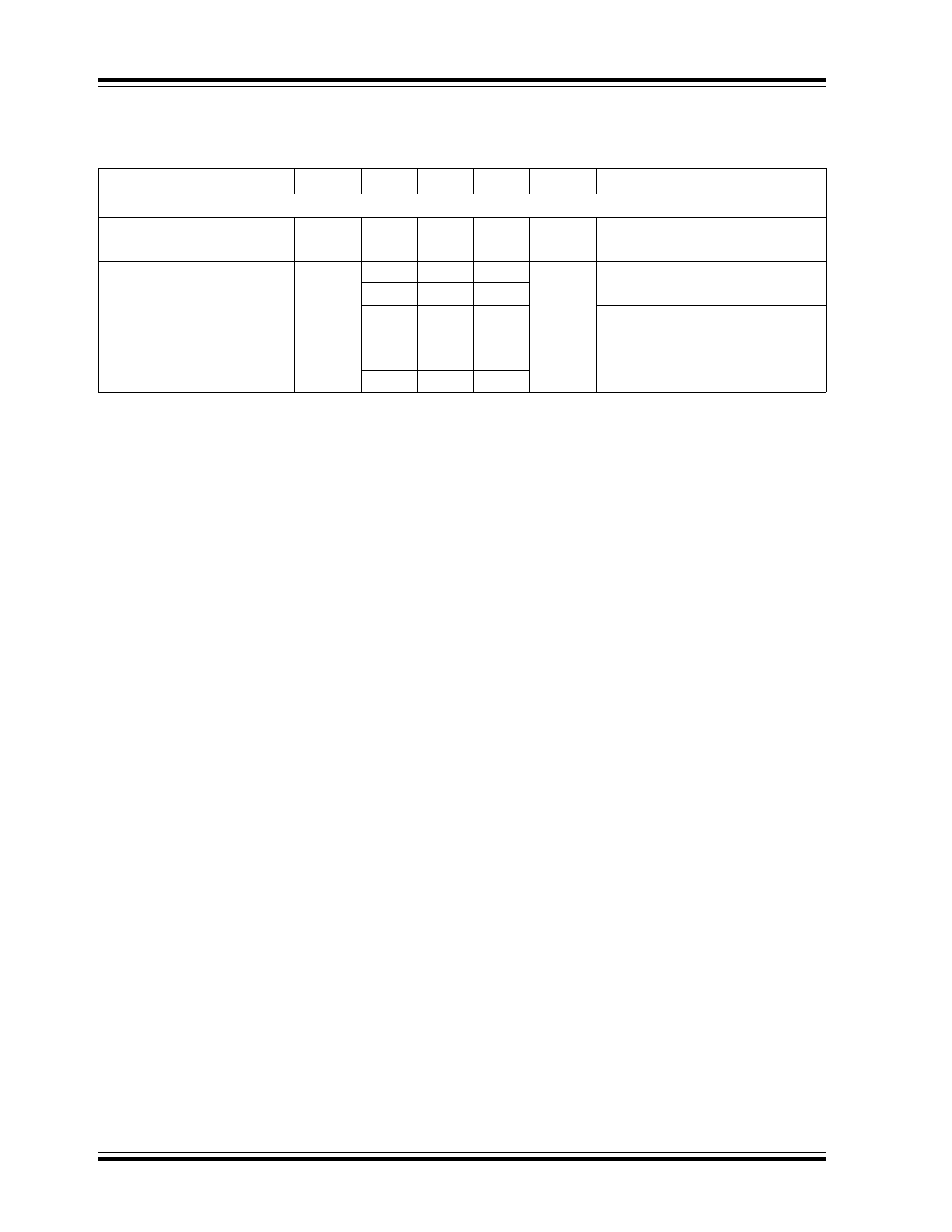
ENABLE Input
Input Logic Voltage
V
ENABLE
—
—
0.8
V
Low (OFF)
2.4
—
—
High (ON)
Enable Pin Input Current
I
ENABLE
—
15
30
µA
V
EN
= 4.2V
—
—
75
—
—
2
V
EN
= 0.8V
—
—
4
Regulator Output Current in
Shutdown
I
OUT-SHDN
—
10
—
µA
Note 5
—
—
20
Note 1:
Specification for packaged product only
2:
Dropout voltage is defined as the input-to-output differential when output voltage drops to 99% of its nor-
mal value with V
OUT
+ 1V applied to V
IN
.
3:
V
IN
= V
OUT
(nominal) + 1V. For example, use V
IN
= 4.3V for a 3.3V regulator or use 6V for a 5V regulator.
Employ pulse testing procedure for current-limit.
4:
V
REF
≤ V
OUT
≤ V
IN
– 1, 3V ≤ V
OUT
≤ 16V, 10 mA ≤ I
L
≤ I
FL
, T
J
≤ T
J(MAX)
.
5:
V
EN
≤ 0.8V, V
IN
≤ 16V and V
OUT
= 0V.
TABLE 1-1:
ELECTRICAL CHARACTERISTICS (CONTINUED)
Electrical Characteristics:
V
IN
= 4.184V; I
OUT
= 100 mA; T
A
= +25°C, bold values indicate –40°C ≤ T
J
≤ +125°C,
unless noted.
Note 1
Parameter
Symbol
Min.
Typ.
Max.
Units
Conditions
2018 Microchip Technology Inc.
DS20005897B-page 5
MIC29302A
TEMPERATURE SPECIFICATIONS (
Note 1
)
Parameters
Sym.
Min.
Typ.
Max.
Units
Conditions
Temperature Ranges
Junction Operating Temperature
Range
T
J
–40
—
+125
°C
—
Storage Temperature Range
T
S
–65
—
+150
°C
—
Package Thermal Resistances
Thermal Resistance TO-263
JC
—
3
—
°C/W
—
Thermal Resistance TO-252
JC
—
3
—
°C/W
—
Thermal Resistance TO-263
JA
—
28
—
°C/W
—
Thermal Resistance TO-252
JA
—
35
—
°C/W
—
Note 1:
The maximum allowable power dissipation is a function of ambient temperature, the maximum allowable
junction temperature and the thermal resistance from junction to air (i.e., T
A
, T
J
,
JA
). Exceeding the
maximum allowable power dissipation will cause the device operating junction temperature to exceed the
maximum +125°C rating. Sustained junction temperatures above +125°C can impact the device reliability.
MIC29302A
DS20005897B-page 6
2018 Microchip Technology Inc.
2.0
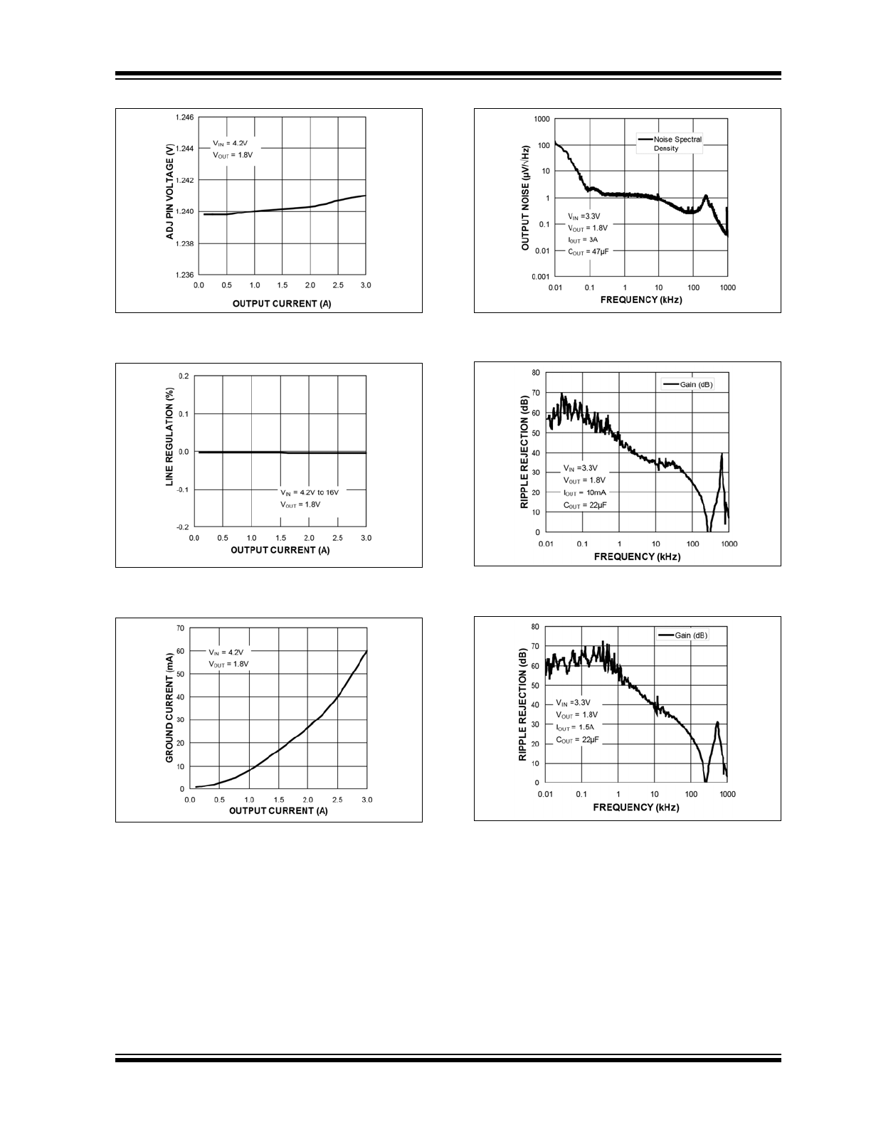
TYPICAL PERFORMANCE CURVES
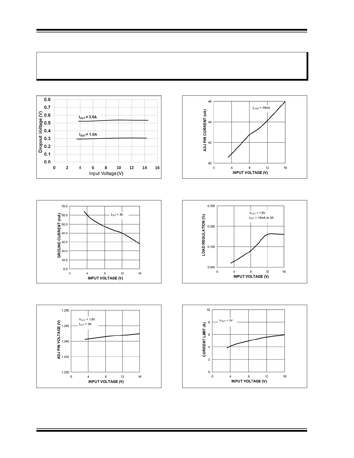
FIGURE 2-1:
Dropout Voltage vs. Input
Voltage.
FIGURE 2-2:
GND Pin Current vs. Input
Voltage.
FIGURE 2-3:
Adjust Pin Voltage vs. Input
Voltage.
FIGURE 2-4:
Adjust Pin Current vs. Input
Voltage.
FIGURE 2-5:
Load Regulation vs. Input
Voltage.
FIGURE 2-6:
Short-Circuit Current vs.
Input Voltage.
Note:
The graphs and tables provided following this note are a statistical summary based on a limited number of
samples and are provided for informational purposes only. The performance characteristics listed herein
are not tested or guaranteed. In some graphs or tables, the data presented may be outside the specified
operating range (e.g., outside specified power supply range) and therefore outside the warranted range.
2018 Microchip Technology Inc.
DS20005897B-page 7
MIC29302A
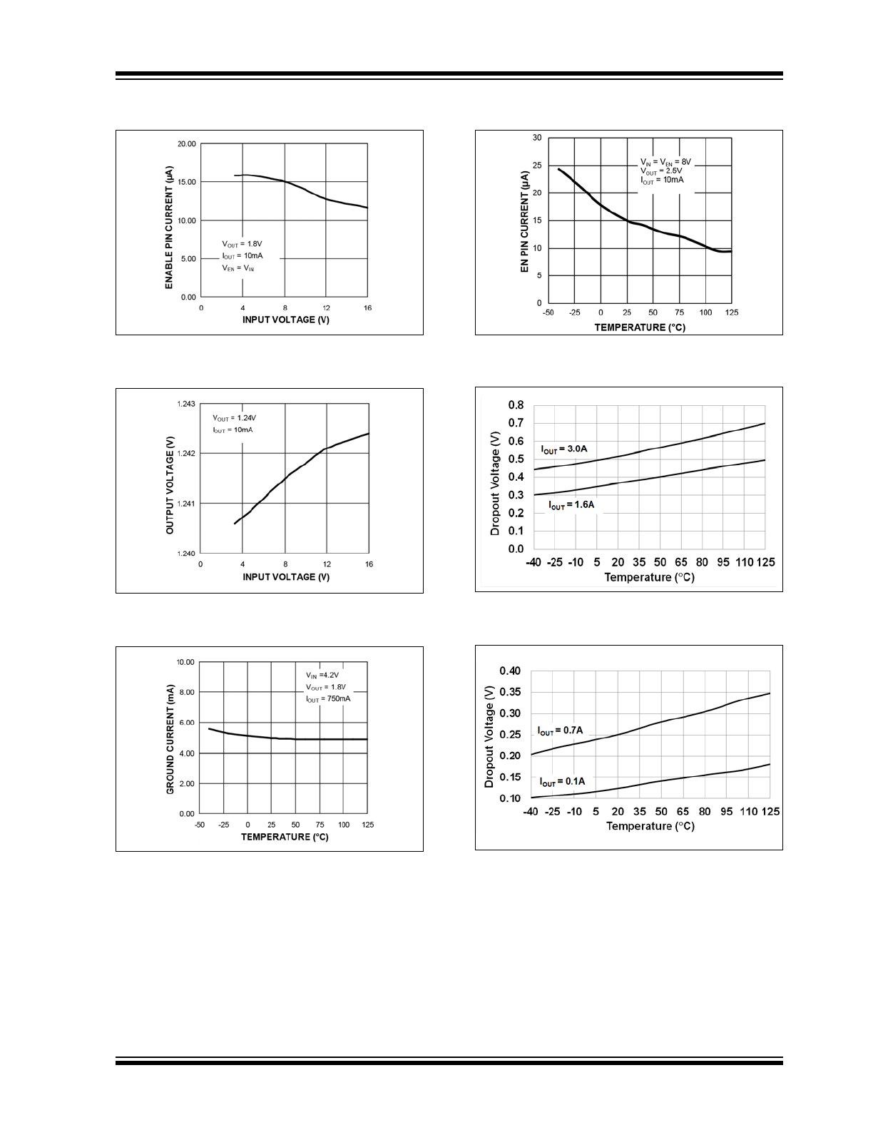
FIGURE 2-7:
Enable Pin Current vs. Input
Voltage.
FIGURE 2-8:
Output Voltage vs. Input
Voltage.
FIGURE 2-9:
GND Pin Current vs.
Temperature.
FIGURE 2-10:
Enable Bias Current vs.
Temperature.
FIGURE 2-11:
Dropout Voltage vs.
Temperature.
FIGURE 2-12:
Dropout Voltage vs.
Temperature.
MIC29302A
DS20005897B-page 8
2018 Microchip Technology Inc.
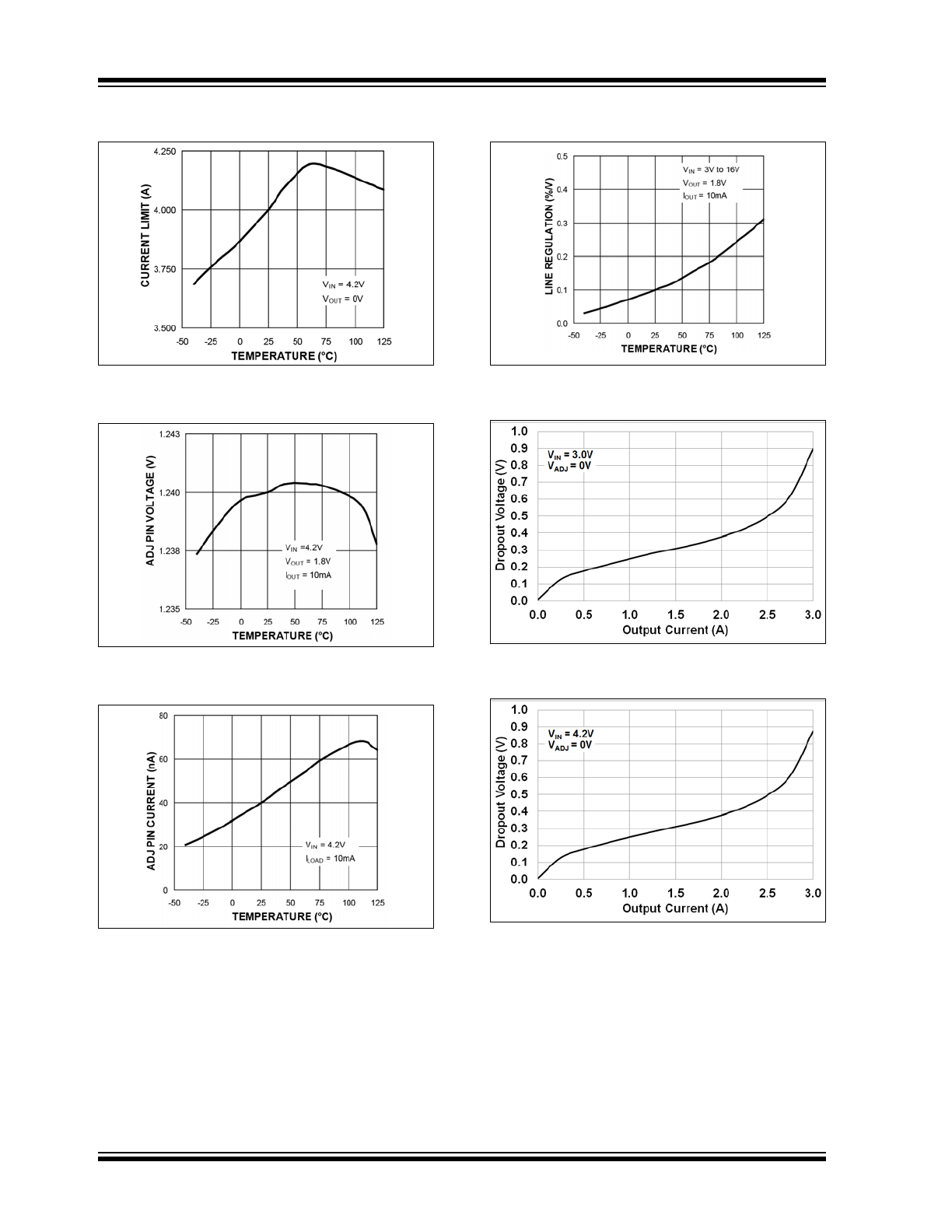
FIGURE 2-13:
Short-Circuit Current vs.
Temperature
.
FIGURE 2-14:
Adjust Pin Voltage vs.
Temperature
.
FIGURE 2-15:
Adjust Pin Current vs.
Temperature.
FIGURE 2-16:
Line Regulation vs.
Temperature.
FIGURE 2-17:
Dropout Voltage vs. Output
Current.
FIGURE 2-18:
Dropout Voltage vs. Output
Current.
2018 Microchip Technology Inc.
DS20005897B-page 9
MIC29302A
FIGURE 2-19:
Adjust Pin Voltage vs.
Output Current.
FIGURE 2-20:
Line Regulation vs. Output
Current.
FIGURE 2-21:
GND Pin Current vs. Output
Current.
FIGURE 2-22:
Output Noise vs. Frequency.
FIGURE 2-23:
Ripple Rejection (I
OUT
=
10 mA) vs. Frequency.
FIGURE 2-24:
Ripple Rejection (I
OUT
=
1.5A) vs. Frequency.
MIC29302A
DS20005897B-page 10
2018 Microchip Technology Inc.
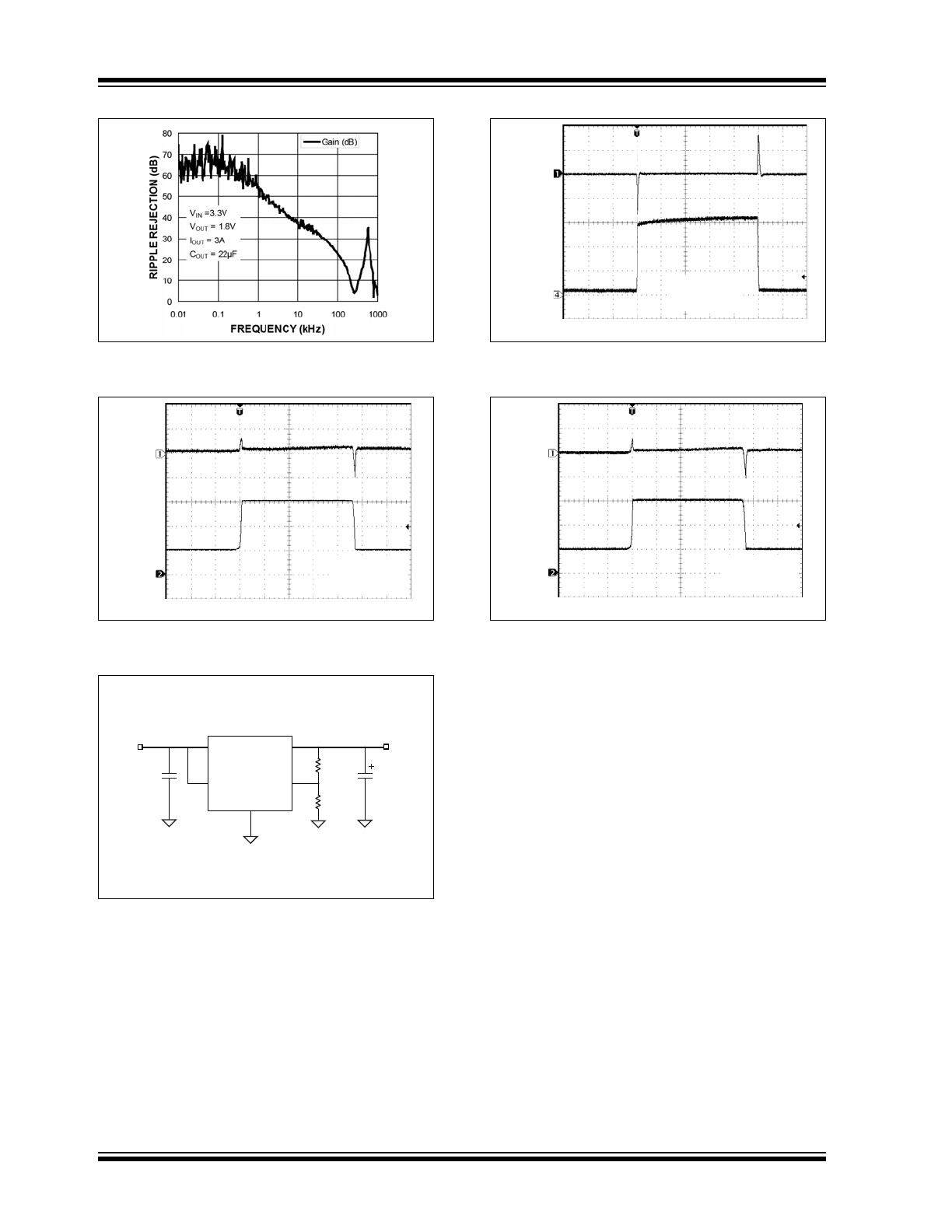
FIGURE 2-25:
Ripple Rejection (I
OUT
= 3A)
vs. Frequency.
FIGURE 2-26:
Line Transient Response
with 3A Load, 1000 µF Output Capacitance.
FIGURE 2-27:
MIC29302A Load Transient
Response Test Circuit.
FIGURE 2-28:
Line Transient Response
with 3A Load, 10 µF Output Capacitance.
FIGURE 2-29:
Load Transient Response
with 3A Load, 1000 µF Output Capacitance.
Time (1.00ms/div)
5V
6mV
11mV
15V
I
OUT
= 3A
C
OUT
= 1000μF
V
OUT
V
IN
3.3V
IN
C
IN
R1
R2
2.5V
OUT
C
L
OUT
IN
EN
ADJ
GND
Time (1.00ms/div)
200mA
32mV
3mV
3A
I
OUT
= 3A
C
OUT
= 1000μF
V
OUT
I
OUT
Time (1.00ms/div)
5V
6mV
11mV
15V
I
OUT
= 3A
C
OUT
= 10μF
V
OUT
V
IN