
© 2007 Microchip Technology Inc.
DS21998B-page 1
TC4423A/TC4424A/TC4425A
Features
• High Peak Output Current: 4.5A (typical)
• Wide Input Supply Voltage Operating Range:
- 4.5V to 18V
• High Capacitive Load Drive Capability:
- 1800 pF in 12 ns
• Short Delay Times: 40 ns (typical)
• Matched Rise/Fall Times
• Low Supply Current:
- With Logic ‘1’ Input – 1.0 mA (maximum)
- With Logic ‘0’ Input – 150 µA (maximum)
• Low Output Impedance: 2.5
Ω (typical)
• Latch-Up Protected: Will Withstand 1.5A Reverse
Current
• Logic Input Will Withstand Negative Swing Up To
5V
• Pin compatible with the TC4423/TC4424/TC4425
and TC4426A/TC4427A/TC4428A devices
• Space-saving 8-Pin 150 mil body SOIC and 8-Pin
6x5 DFN Packages
Applications
• Switch Mode Power Supplies
• Pulse Transformer Drive
• Line Drivers
• Direct Drive of Small DC Motors
General Description
The TC4423A/TC4424A/TC4425A devices are a family
of dual-output 3A buffers/MOSFET drivers. These
devices are improved versions of the earlier TC4423/
TC4424/TC4425 dual-output 3A driver family. This
improved version features higher peak output current
drive capability, lower shoot-throught current, matched
rise/fall times and propagation delay times. The
TC4423A/TC4424A/TC4425A devices are pin-
compatible with the existing TC4423/TC4424/TC4425
family. An 8-pin SOIC package option has been added
to the family. The 8-pin DFN package option offers
increased power dissipation capability for driving
heavier capacitive or resistive loads.
The TC4423A/TC4424A/TC4425A MOSFET drivers
can easily charge and discharge 1800 pF gate
capacitance in under 20 ns, provide low enough
impedances in both the on and off states to ensure the
MOSFET’s intended state will not be affected, even by
large transients.
The TC4423A/TC4424A/TC4425A inputs may be
driven directly from either TTL or CMOS (2.4V to 18V).
In addition, the 300 mV of built-in hysteresis provides
noise immunity and allows the device to be driven from
slow rising or falling waveforms.
The TC4423A/TC4424A/TC4425A dual-output 3A
MOSFET driver family is offerd with a -40
o
C to +125
o
C
temperature rating, making it useful in any wide
temperature range application.
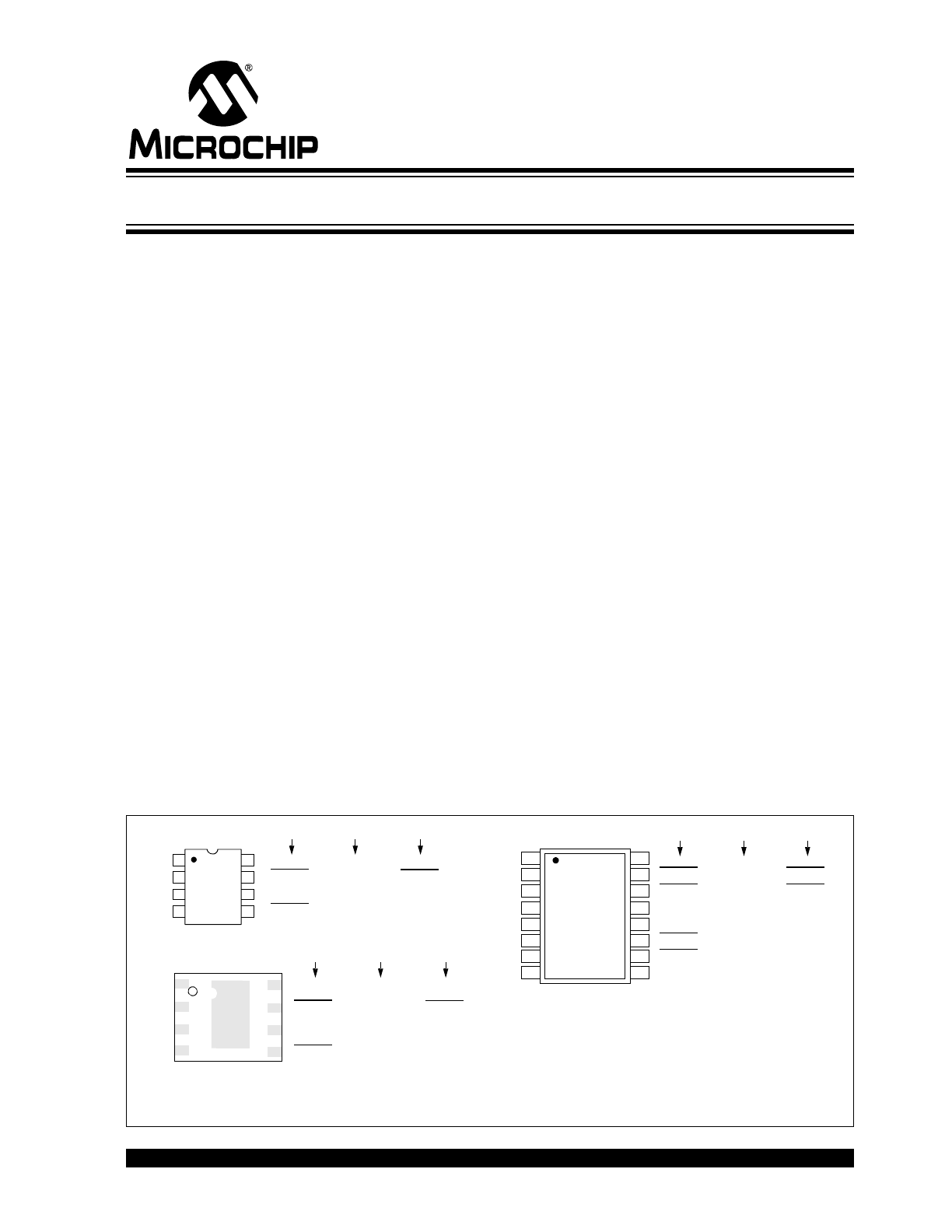
Package Types
NC
IN A
GND
IN B
2
3
4
5
6
7
8
1
1
2
3
4
NC
5
6
7
8
OUT A
OUT B
NC
IN A
GND
IN B
V
DD
TC4423A
TC4424A
Note 1: Exposed pad of the DFN package is electrically isolated.
2: Duplicate pins must both be connected for proper operation
.
TC4423A TC4424A
NC
OUT A
OUT B
V
DD
TC4423A
TC4424A
TC4425A
NC
OUT A
OUT B
V
DD
TC4425A
TC4425A
NC
OUT A
OUT B
V
DD
TC4423A TC4424A
NC
OUT A
OUT B
V
DD
TC4425A
NC
OUT A
OUT B
V
DD
8-Pin PDIP/SOIC
8-Pin 6x5 DFN
(1
)
1
2
3
4
5
6
7
8
16
13
12
11
10
9
NC
IN A
NC
GND
GND
NC
IN B
NC
NC
OUT A
V
DD
V
DD
OUT B
OUT B
NC
OUT A
15
14
TC4423A
TC4424A
TC4425A
16-Pin SOIC (Wide
)
NC
OUT A
V
DD
V
DD
OUT B
OUT B
NC
OUT A
OUT A
V
DD
V
DD
OUT B
OUT B
NC
OUT A
TC4423A TC4424A TC4425A
NC
3A Dual High-Speed Power MOSFET Drivers
TC4423A/TC4424A/TC4425A
DS21998B-page 2
© 2007 Microchip Technology Inc.
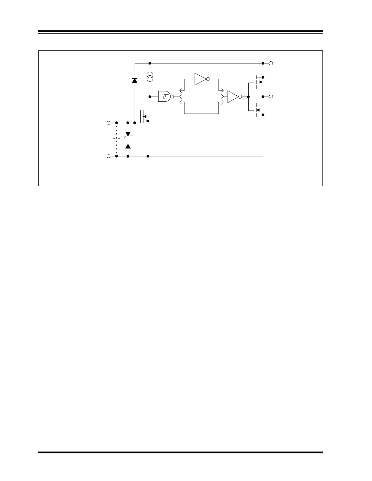
Functional Block Diagram
(1)
Effective
Input C = 20 pF
(Each Input)
TC4423A Dual Inverting
TC4424A Dual Non-inverting
TC4425A Inverting / Non-inverting
Output
Input
GND
V
DD
300 mV
4.7V
Inverting
Non-inverting
Note 1: Unused inputs should be grounded.
750 µA
© 2007 Microchip Technology Inc.
DS21998B-page 3
TC4423A/TC4424A/TC4425A
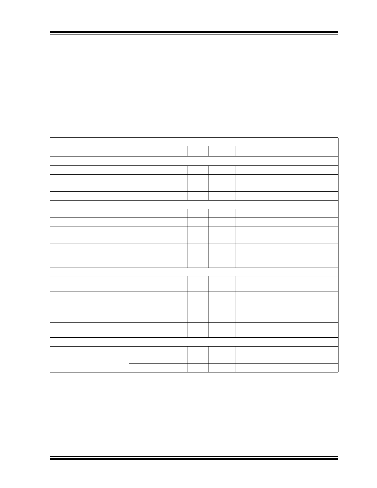
1.0
ELECTRICAL
CHARACTERISTICS
Absolute Maximum Ratings †
Supply Voltage ................................................................+20V
Input Voltage, IN A or IN B ..........(V
DD
+ 0.3V) to (GND – 5V)
Package Power Dissipation (T
A
=50°C)
8L PDIP .......................................................................1.2W
8L SOIC.................................................................... 0.61W
16L SOIC.....................................................................1.1W
8L DFN .................................................................... Note 3
† Notice: Stresses above those listed under "Maximum
Ratings" may cause permanent damage to the device. This is
a stress rating only and functional operation of the device at
those or any other conditions above those indicated in the
operational sections of this specification is not intended.
Exposure to maximum rating conditions for extended periods
may affect device reliability.
DC CHARACTERISTICS (NOTE 2)
Electrical Specifications: Unless otherwise indicated, T
A
= +25°C, with 4.5V
≤ V
DD
≤ 18V.
Parameters
Sym
Min
Typ
Max
Units
Conditions
Input
Logic ‘1’, High Input Voltage
V
IH
2.4
1.5
—
V
Logic ‘0’, Low Input Voltage
V
IL
—
1.3
0.8
V
Input Current
I
IN
–1
—
1
µA
0V
≤ V
IN
≤ V
DD
Input Voltage
V
IN
-5
—
V
DD
+0.3
V
Output
High Output Voltage
V
OH
V
DD
– 0.025
—
—
V
DC Test
Low Output Voltage
V
OL
—
—
0.025
V
DC Test
Output Resistance, High
R
OH
—
2.2
3.0
Ω
I
OUT
= 10 mA, V
DD
= 18V
Output Resistance, Low
R
OL
—
2.8
3.5
Ω
I
OUT
= 10 mA, V
DD
= 18V
Peak Output Current
I
PK
—
4.5
—
A
10V
≤ V
DD
≤18V (Note 2)
Latch-Up Protection With-
stand Reverse Current
I
REV
—
>1.5
—
A
Duty cycle
≤ 2%, t ≤ 300 µsec.
Switching Time (Note 1)
Rise Time
t
R
—
12
21
ns
Figure 4-1, Figure 4-2,
C
L
= 1800 pF
Fall Time
t
F
—
12
21
ns
Figure 4-1, Figure 4-2,
C
L
= 1800 pF
Delay Time
t
D1
—
40
48
ns
Figure 4-1, Figure 4-2,
C
L
= 1800 pF
Delay Time
t
D2
—
41
48
ns
Figure 4-1, Figure 4-2,
C
L
= 1800 pF
Power Supply
Supply Voltage
V
DD
4.5
—
18
V
Power Supply Current
I
S
—
1.0
2.0
mA
V
IN
= 3V (Both inputs)
I
S
—
0.15
0.25
mA
V
IN
= 0V (Both inputs)
Note 1: Switching times ensured by design.
2: Tested during characterization, not production tested.
3: Package power dissipation is dependent on the copper pad area on the PCB.
TC4423A/TC4424A/TC4425A
DS21998B-page 4
© 2007 Microchip Technology Inc.
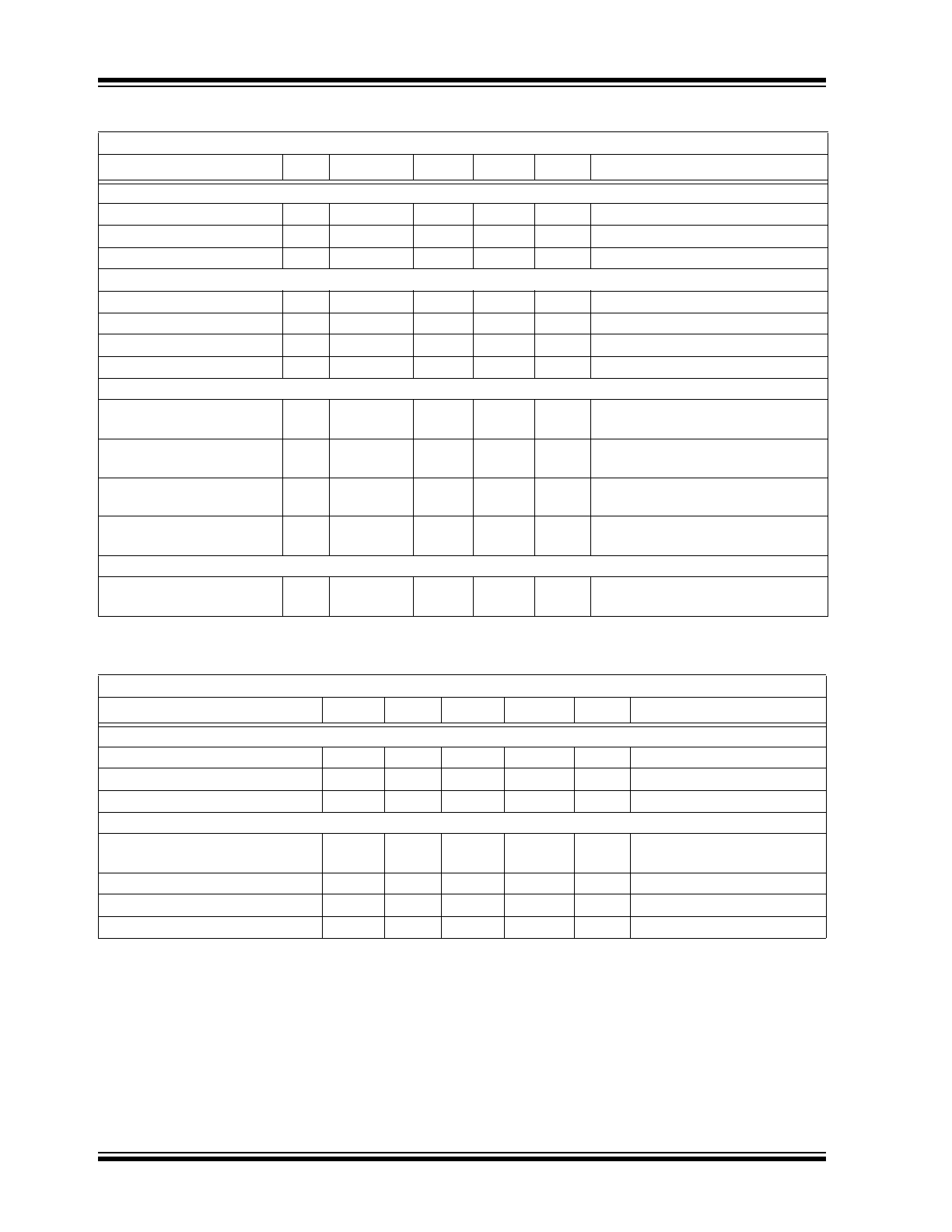
DC CHARACTERISTICS (OVER OPERATING TEMPERATURE RANGE)
TEMPERATURE CHARACTERISTICS
Electrical Specifications: Unless otherwise indicated, operating temperature range with 4.5V
≤ V
DD
≤ 18V.
Parameters
Sym
Min
Typ
Max
Units
Conditions
Input
Logic ‘1’, High Input Voltage
V
IH
2.4
—
—
V
Logic ‘0’, Low Input Voltage
V
IL
—
—
0.8
V
Input Current
I
IN
–10
—
+10
µA
0V
≤ V
IN
≤ V
DD
Output
High Output Voltage
V
OH
V
DD
– 0.025
—
—
V
Low Output Voltage
V
OL
—
—
0.025
V
Output Resistance, High
R
OH
—
3.1
6
Ω
I
OUT
= 10 mA, V
DD
= 18V
Output Resistance, Low
R
OL
—
3.7
7
Ω
I
OUT
= 10 mA, V
DD
= 18V
Switching Time (Note 1)
Rise Time
t
R
—
20
31
ns
Figure 4-1, Figure 4-2,
C
L
= 1800 pF
Fall Time
t
F
—
22
31
ns
Figure 4-1, Figure 4-2,
C
L
= 1800 pF
Delay Time
t
D1
—
50
66
ns
Figure 4-1, Figure 4-2,
C
L
= 1800 pF
Delay Time
t
D2
—
50
66
ns
Figure 4-1, Figure 4-2,
C
L
= 1800 pF
Power Supply
Power Supply Current
I
S
—
—
2.0
0.2
3.0
0.3
mA
V
IN
= 3V (Both inputs)
V
IN
= 0V (Both inputs)
Note 1: Switching times ensured by design.
Electrical Specifications: Unless otherwise noted, all parameters apply with 4.5V
≤ V
DD
≤ 18V.
Parameters
Sym
Min
Typ
Max
Units
Conditions
Temperature Ranges
Specified Temperature Range (V)
T
A
–40
—
+125
°C
Maximum Junction Temperature
T
J
—
—
+150
°C
Storage Temperature Range
T
A
–65
—
+150
°C
Package Thermal Resistances
Thermal Resistance, 8L-6x5 DFN
θ
JA
—
33.2
—
°C/W
Typical four-layer board with
vias to ground plane
Thermal Resistance, 8L-PDIP
θ
JA
—
84.6
—
°C/W
Thermal Resistance, 8L-SOIC
θ
JA
—
163
—
°C/W
Thermal Resistance, 16L-SOIC
θ
JA
—
90
—
°C/W
© 2007 Microchip Technology Inc.
DS21998B-page 5
TC4423A/TC4424A/TC4425A
2.0
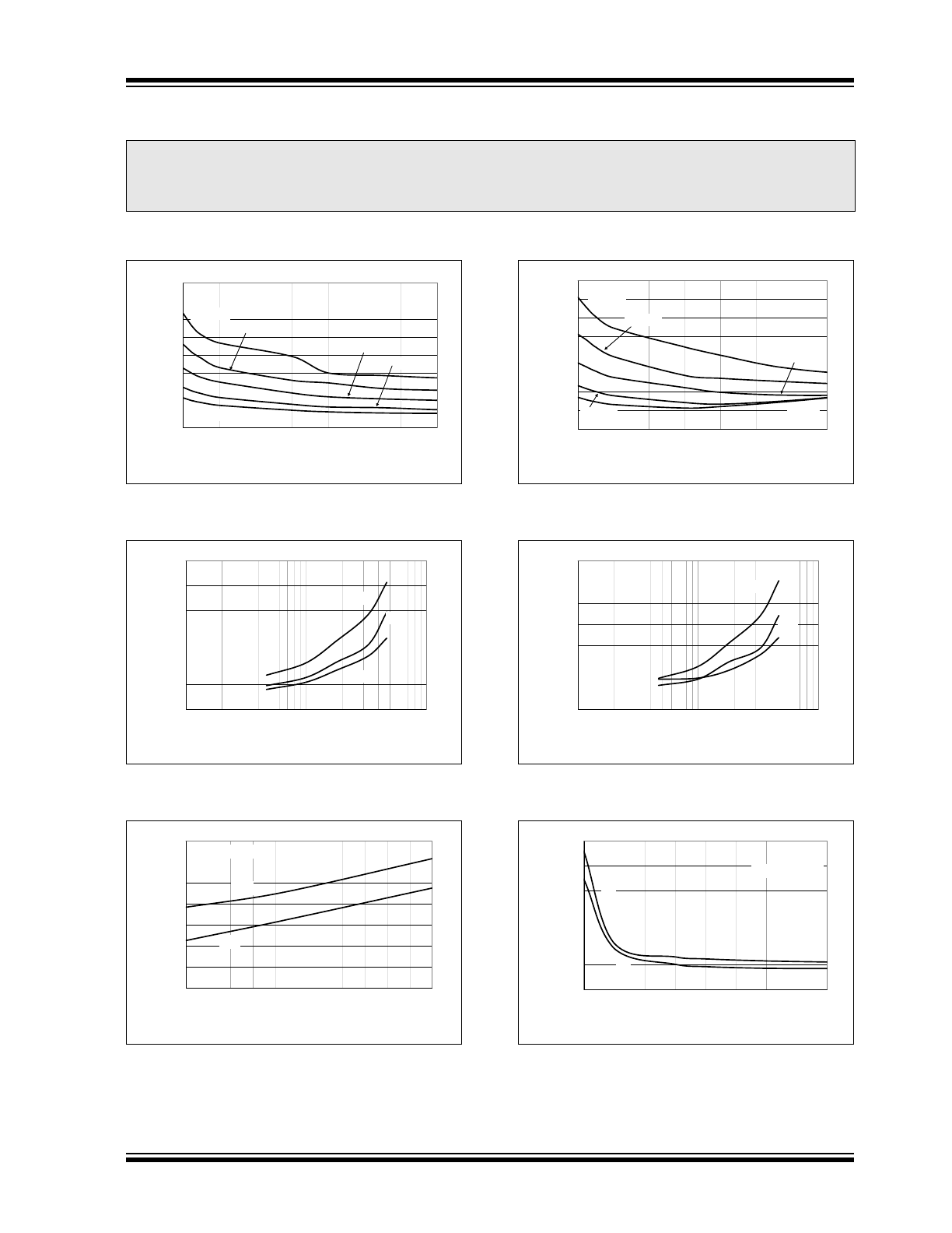
TYPICAL PERFORMANCE CURVES
Note: Unless otherwise indicated, T
A
= +25°C with 4.5V <= V
DD
<= 18V.
FIGURE 2-1:
Rise Time vs. Supply
Voltage.
FIGURE 2-2:
Rise Time vs. Capacitive
Load.
FIGURE 2-3:
Rise and Fall Times vs.
Temperature.
FIGURE 2-4:
Fall Time vs. Supply
Voltage.
FIGURE 2-5:
Fall Time vs. Capacitive
Load.
FIGURE 2-6:
Propagation Delay vs. Input
Amplitude.
Note:
The graphs and tables provided following this note are a statistical summary based on a limited number of
samples and are provided for informational purposes only. The performance characteristics listed herein
are not tested or guaranteed. In some graphs or tables, the data presented may be outside the specified
operating range (e.g., outside specified power supply range) and therefore outside the warranted range.
0
10
20
30
40
50
60
70
80
4
6
8
10
12
14
16
18
Supply Voltage (V)
R
ise Ti
me
(
n
s)
4,700 pF
3,300 pF
1,800 pF
1,000 pF
470 pF
0
10
20
30
40
50
60
100
1000
10000
Capacitive Load (pF)
R
ise
T
im
e (n
s)
5V
10V
15V
10
12
14
16
18
20
22
24
-40 -25 -10 5
20 35 50 65 80 95 110 125
Temperature (
o
C)
Time (ns
)
t
FALL
t
RISE
C
LOAD
= 1800 pF
0
10
20
30
40
50
60
70
80
4
6
8
10
12
14
16
18
Supply Voltage (V)
F
all
T
im
e (n
s)
4700 pF
3300 pF
1800 pF
470 pF
1000 pF
0
10
20
30
40
50
60
70
100
1000
10000
Capacitive Load (pF)
F
a
ll
Tim
e (
n
s)
5V
10V
15V
25
45
65
85
105
125
145
2
3
4
5
6
7
8
9
10
Input Amplitude (V)
Propa
ga
ti
o
n
De
la
y
(n
s)
t
D1
t
D2
V
DD
= 12V
C
LOAD
= 1800 pF
TC4423A/TC4424A/TC4425A
DS21998B-page 6
© 2007 Microchip Technology Inc.
Typical Performance Curves (Continued)
Note: Unless otherwise indicated, T
A
= +25°C with 4.5V <= V
DD
<= 18V.
FIGURE 2-7:
Propagation Delay Time vs.
Supply Voltage.
FIGURE 2-8:
Quiescent Current vs.
Supply Voltage.
FIGURE 2-9:
Output Resistance (Output
Low) vs. Supply Voltage.
FIGURE 2-10:
Propagation Delay Time vs.
Temperature.
FIGURE 2-11:
Quiescent Current vs.
Temperature.
FIGURE 2-12:
Output Resistance (Output
High) vs. Supply Voltage.
30
40
50
60
70
80
90
100
4
6
8
10
12
14
16
18
Supply Voltage (V)
P
rop
ag
ati
o
n
D
e
la
y
(ns
)
t
D1
t
D2
C
LOAD
= 1800 pF
0
0.1
0.2
0.3
0.4
0.5
4
6
8
10
12
14
16
18
Supply Voltage (V)
Q
u
ie
sc
e
n
t Curre
nt (m
A)
Both Inputs = 1
Both Inputs = 0
V
DD
= 18V
1
2
3
4
5
6
7
4
6
8
10
12
14
16
18
Supply Voltage (V)
R
OUT-LO
(
::
)
T
J
= 150
o
C
T
J
= 25
o
C
V
IN
= 5V (TC4424A)
V
IN
= 0V (TC4423A)
30
35
40
45
50
55
60
65
70
-40 -25 -10
5
20 35 50 65 80 95 110 125
Temperature (
o
C)
Pro
p
a
g
atio
n
De
lay
(n
s)
t
D1
t
D2
C
LOAD
= 1800 pF
V
DD
= 18V
V
IN
= 5V
0
0.1
0.2
0.3
0.4
0.5
-40 -25 -10
5
20 35 50 65 80 95 110 125
Temperature (
o
C)
Q
u
ie
sce
nt C
u
rr
en
t (m
A)
Both Inputs = 1
Both Inputs = 0
V
DD
= 18V
2
3
4
5
6
7
8
4
6
8
10
12
14
16
18
Supply Voltage (V)
R
OUT-HI
(
::
)
T
J
= 150
o
C
T
J
= 25
o
C
V
IN
= 0V (TC4424A)
V
IN
= 5V (TC4423A)
© 2007 Microchip Technology Inc.
DS21998B-page 7
TC4423A/TC4424A/TC4425A
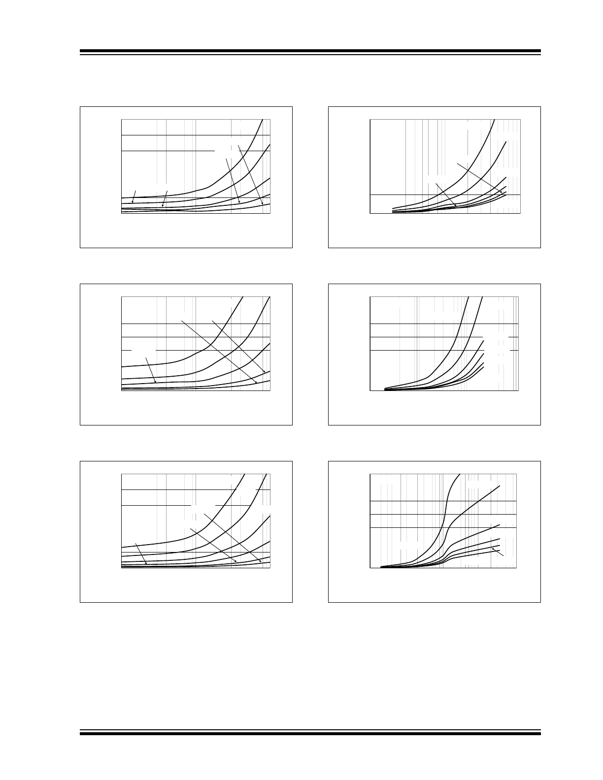
Typical Performance Curves (Continued)
Note: Unless otherwise indicated, T
A
= +25°C with 4.5V <= V
DD
<= 18V.
FIGURE 2-13:
Supply Current vs.
Capacitive Load.
FIGURE 2-14:
Supply Current vs.
Capacitive Load.
FIGURE 2-15:
Supply Current vs.
Capacitive Load.
FIGURE 2-16:
Supply Current vs.
Frequency.
FIGURE 2-17:
Supply Current vs.
Frequency.
FIGURE 2-18:
Supply Current vs.
Frequency.
0
20
40
60
80
100
120
100
1000
10000
Capacitive Load (pF)
S
u
ppl
y Cu
rre
n
t (mA
)
400 kHz
100 kHz
50 kHz
650 kHz
200 kHz
V
DD
= 18V
0
20
40
60
80
100
120
140
100
1000
10000
Capacitive Load (pF)
S
u
ppl
y Cu
rre
n
t (mA
)
500 kHz
200 kHz
1 MHz
2 MHz
100 kHz
V
DD
= 12V
0
20
40
60
80
100
120
100
1000
10000
Capacitive Load (pF)
S
u
ppl
y Cu
rre
n
t (mA
)
500 kHz
2 MHz
1 MHz
3.5 MHz
100 kHz
V
DD
= 6V
200 kHz
0
10
20
30
40
50
60
70
80
90
100
10
100
1000
Frequency (kHz)
S
u
ppl
y Cu
rre
n
t (mA
)
4,700 pF
1,000 pF
470 pF
100 pF
1,800 pF
V
DD
= 18V
10,000 pF
0
20
40
60
80
100
120
140
10
100
1000
10000
Frequency (kHz)
S
u
ppl
y Cu
rre
n
t (mA
)
4,700 pF
1,000 pF
470 pF
100 pF
1,800 pF
V
DD
= 12V
10,000 pF
0
20
40
60
80
100
120
140
10
100
1000
10000
100000
Frequency (kHz)
S
u
ppl
y Cu
rre
n
t (mA
)
4,700 pF
1,000 pF
470 pF
100 pF
1,800 pF
V
DD
= 6V
10,000 pF
TC4423A/TC4424A/TC4425A
DS21998B-page 8
© 2007 Microchip Technology Inc.
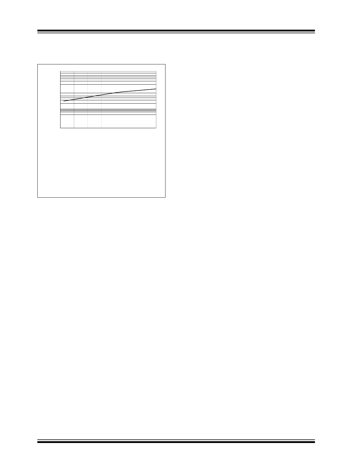
Typical Performance Curves (Continued)
Note: Unless otherwise indicated, T
A
= +25°C with 4.5V <= V
DD
<= 18V.
FIGURE 2-19:
Crossover Energy vs.
Supply Voltage.
1.00E-09
1.00E-08
1.00E-07
1.00E-06
4
6
8
10
12
14
16
18
Supply Voltage (V)
Cros
sove
r E
n
ergy
(A
*se
c
)
10
-6
10
-7
10
-8
10
-9
Note:
The values on this graph
represents the loss seen by both
drivers in a package during one
complete cycle. For a single driver,
divide the stated values by 2. For a
single transition of a single driver,
divide the stated value by 4.
© 2007 Microchip Technology Inc.
DS21998B-page 9
TC4423A/TC4424A/TC4425A
3.0
PIN DESCRIPTIONS
The descriptions of the pins are listed in Table 3-1.
TABLE 3-1:
PIN FUNCTION TABLE
(1)
3.1
Inputs A and B
Inputs A and B are TTL/CMOS compatible inputs that
control outputs A and B, respectively. These inputs
have 300 mV of hysteresis between the high and low
input levels, allowing them to be driven from slow rising
and falling signals, and to provide noise immunity.
3.2
Outputs A and B
Outputs A and B are CMOS push-pull outputs that are
capable of sourcing and sinking 3A peaks of current
(V
DD
= 18V). The low output impedance ensures the
gate of the external MOSFET will stay in the intended
state even during large transients. These outputs also
have a reverse current latch-up rating of 1.5A.
3.3
Supply Input (V
DD
)
V
DD
is the bias supply input for the MOSFET driver and
has a voltage range of 4.5V to 18V. This input must be
decoupled to ground with a local ceramic capacitor.
This bypass capacitor provides a localized low-
impedance path for the peak currents that are to be
provided to the load.
3.4
Ground (GND)
Ground is the device return pin. The ground pin should
have a low-impedance connection to the bias supply
source return. High peak currents will flow out the
ground pin when the capacitive load is being
discharged.
3.5
Exposed Metal Pad
The exposed metal pad of the DFN package is not
internally connected to any potential. Therefore, this
pad can be connected to a ground plane or other
copper plane on a printed circuit board to aid in heat
removal from the package.
8-Pin PDIP
8-Pin
DFN
16-Pin
SOIC
(Wide)
Symbol
Description
1
1
1
NC
No connection
2
2
2
IN A
Input A
—
—
3
NC
No connection
3
3
4
GND
Ground
—
—
5
GND
Ground
—
—
6
NC
No connection
4
4
7
IN B
Input B
—
—
8
NC
No connection
—
—
9
NC
No connection
5
5
10
OUT B
Output B
—
—
11
OUT B
Output B
6
6
12
V
DD
Supply input
—
—
13
V
DD
Supply input
7
7
14
OUT A
Output A
—
—
15
OUT A
Output A
8
8
16
NC
No connection
—
PAD
—
NC
Exposed Metal Pad
Note 1: Duplicate pins must be connected for proper operation.
TC4423A/TC4424A/TC4425A
DS21998B-page 10
© 2007 Microchip Technology Inc.
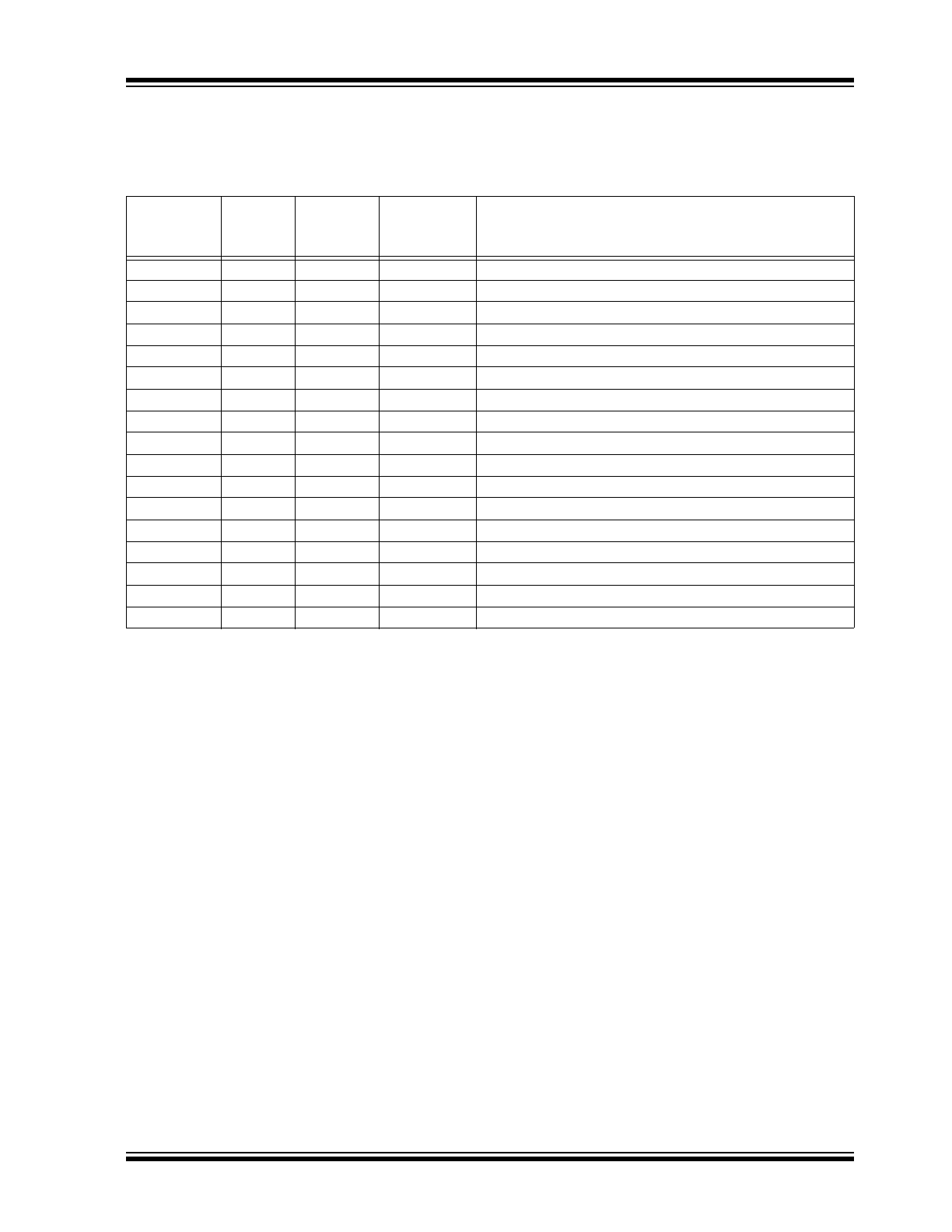
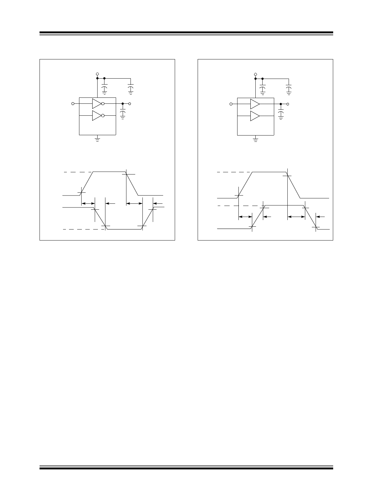
4.0
APPLICATIONS INFORMATION
FIGURE 4-1:
Inverting Driver Switching
Time.
FIGURE 4-2:
Non-inverting Driver
Switching Time.
0.1 µF
+5V
10%
90%
10%
90%
10%
90%
18V
1 µF
WIMA
MKS-2
0V
0V
TC4423A
(1/2 TC4425A)
1
2
C
L
= 1800 pF
Input
Input
Output
t
D1
t
F
t
D2
Input: 100 kHz,
square wave,
Output
t
R
V
DD
= 18V
t
RISE
= t
FALL
≤ 10 ns
Ceramic
90%
Input
t
D1
t
F
t
D2
Output
t
R
10%
10%
10%
+5V
18V
0V
0V
90%
90%
Input: 100 kHz,
square wave,
t
RISE
= t
FALL
≤ 10 ns
0.1 µF
1 µF
WIMA
MKS-2
TC4424A
(1/2 TC4425A)
1
2
C
L
= 1800 pF
Input
Output
V
DD
= 18V
Ceramic