
2001-2013 Microchip Technology Inc.
DS35007C-page 1
PIC16F84A
High Performance RISC CPU Features:
• Only 35 single word instructions to learn
• All instructions single-cycle except for program
branches which are two-cycle
• Operating speed: DC - 20 MHz clock input
DC - 200 ns instruction cycle
• 1024 words of program memory
• 68 bytes of Data RAM
• 64 bytes of Data EEPROM
• 14-bit wide instruction words
• 8-bit wide data bytes
• 15 Special Function Hardware registers
• Eight-level deep hardware stack
• Direct, indirect and relative addressing modes
• Four interrupt sources:
- External RB0/INT pin
- TMR0 timer overflow
- PORTB<7:4> interrupt-on-change
- Data EEPROM write complete
Peripheral Features:
• 13 I/O pins with individual direction control
• High current sink/source for direct LED drive
- 25 mA sink max. per pin
- 25 mA source max. per pin
• TMR0: 8-bit timer/counter with 8-bit
programmable prescaler
Special Microcontroller Features:
• 10,000 erase/write cycles Enhanced FLASH
Program memory typical
• 10,000,000 typical erase/write cycles EEPROM
Data memory typical
• EEPROM Data Retention > 40 years
• In-Circuit Serial Programming™ (ICSP™) - via
two pins
• Power-on Reset (POR), Power-up Timer (PWRT),
Oscillator Start-up Timer (OST)
• Watchdog Timer (WDT) with its own On-Chip RC
Oscillator for reliable operation
• Code protection
• Power saving SLEEP mode
• Selectable oscillator options
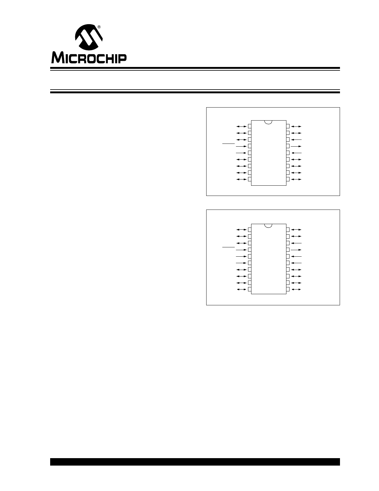
Pin Diagrams
CMOS Enhanced FLASH/EEPROM
Technology:
• Low power, high speed technology
• Fully static design
• Wide operating voltage range:
- Commercial: 2.0V to 5.5V
- Industrial:
2.0V to 5.5V
• Low power consumption:
- < 2 mA typical @ 5V, 4 MHz
- 15
A typical @ 2V, 32 kHz
- < 0.5
A typical standby current @ 2V
RA1
RA0
OSC1/CLKIN
OSC2/CLKOUT
V
DD
RB7
RB6
RB5
RB4
RA2
RA3
RA4/T0CKI
MCLR
V
SS
RB0/INT
RB1
RB2
RB3
1
2
3
4
5
6
7
8
9
18
17
16
15
14
13
12
11
10
PDIP, SOIC
PIC
16F
84A
RA1
RA0
OSC1/CLKIN
OSC2/CLKOUT
V
DD
RB7
RB6
RB5
RB4
RA2
RA3
RA4/T0CKI
MCLR
V
SS
RB0/INT
RB1
RB2
RB3
1
2
3
4
5
6
7
8
9
20
19
18
17
16
15
14
13
12
SSOP
PIC16
F
84
A
10
11
V
SS
V
DD
18-pin Enhanced FLASH/EEPROM 8-Bit Microcontroller

PIC16F84A
DS35007C-page 2
2001-2013 Microchip Technology Inc.
Table of Contents
1.0
Device Overview .......................................................................................................................................................................... 3
2.0
Memory Organization ................................................................................................................................................................... 5
3.0
Data EEPROM Memory ............................................................................................................................................................. 13
4.0
I/O Ports ..................................................................................................................................................................................... 15
5.0
Timer0 Module ........................................................................................................................................................................... 19
6.0
Special Features of the CPU ...................................................................................................................................................... 21
7.0
Instruction Set Summary ............................................................................................................................................................ 35
8.0
Development Support................................................................................................................................................................. 43
9.0
Electrical Characteristics ............................................................................................................................................................ 47
10.0 DC/AC Characteristic Graphs .................................................................................................................................................... 59
11.0 Packaging Information................................................................................................................................................................ 69
Appendix A: Revision History .............................................................................................................................................................. 77
Appendix B: Conversion Considerations.............................................................................................................................................. 78
Appendix C: Migration from Baseline to
Mid-range Devices80
INDEX .................................................................................................................................................................................................. 81
The Microchip Web Site ....................................................................................................................................................................... 85
Customer Change Notification Service ................................................................................................................................................ 85
Customer Support ................................................................................................................................................................................ 85
Reader Response ................................................................................................................................................................................ 86
PIC16F84A Product Identification System ........................................................................................................................................... 87
TO OUR VALUED CUSTOMERS
It is our intention to provide our valued customers with the best documentation possible to ensure successful use of your Microchip
products. To this end, we will continue to improve our publications to better suit your needs. Our publications will be refined and
enhanced as new volumes and updates are introduced.
If you have any questions or comments regarding this publication, please contact the Marketing Communications Department via
E-mail at
docerrors@microchip.com
or fax the Reader Response Form in the back of this data sheet to (480) 792-4150. We
welcome your feedback.
Most Current Data Sheet
To obtain the most up-to-date version of this data sheet, please register at our Worldwide Web site at:
http://www.microchip.com
You can determine the version of a data sheet by examining its literature number found on the bottom outside corner of any page.
The last character of the literature number is the version number, (e.g., DS30000A is version A of document DS30000).
Errata
An errata sheet, describing minor operational differences from the data sheet and recommended workarounds, may exist for current
devices. As device/documentation issues become known to us, we will publish an errata sheet. The errata will specify the revision
of silicon and revision of document to which it applies.
To determine if an errata sheet exists for a particular device, please check with one of the following:
• Microchip’s Worldwide Web site;
http://www.microchip.com
• Your local Microchip sales office (see last page)
When contacting a sales office, please specify which device, revision of silicon and data sheet (include literature number) you are
using.
Customer Notification System
Register on our web site at
www.microchip.com
to receive the most current information on all of our products.
2001-2013 Microchip Technology Inc.
DS35007C-page 3
PIC16F84A
1.0
DEVICE OVERVIEW
This document contains device specific information for
the operation of the PIC16F84A device. Additional
information may be found in the PIC
®
Mid-Range Ref-
erence Manual, (DS33023), which may be downloaded
from the Microchip website. The Reference Manual
should be considered a complementary document to
this data sheet, and is highly recommended reading for
a better understanding of the device architecture and
operation of the peripheral modules.
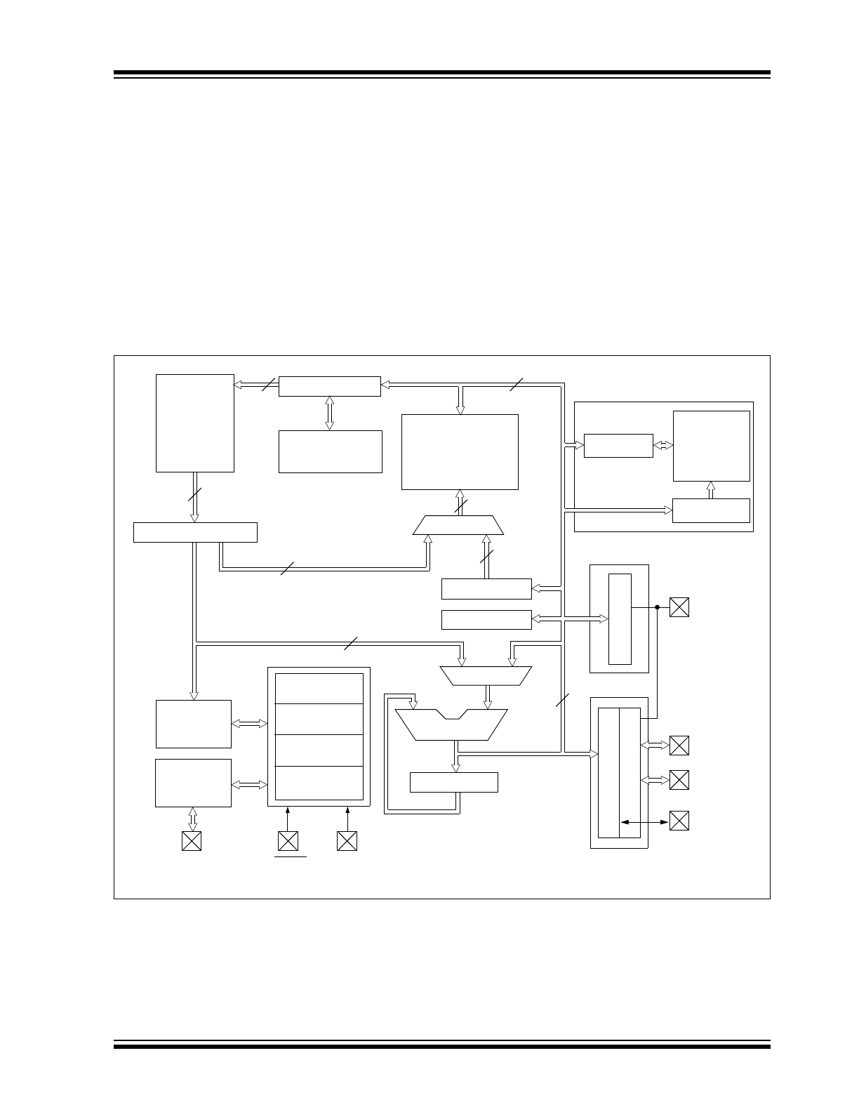
The PIC16F84A belongs to the mid-range family of the
PIC
®
microcontroller devices. A block diagram of the
device is shown in Figure 1-1.
The program memory contains 1K words, which trans-
lates to 1024 instructions, since each 14-bit program
memory word is the same width as each device instruc-
tion. The data memory (RAM) contains 68 bytes. Data
EEPROM is 64 bytes.
There are also 13 I/O pins that are user-configured on
a pin-to-pin basis. Some pins are multiplexed with other
device functions. These functions include:
• External interrupt
• Change on PORTB interrupt
• Timer0 clock input
Table 1-1 details the pinout of the device with descrip-
tions and details for each pin.
FIGURE 1-1:
PIC16F84A BLOCK DIAGRAM
FLASH
Program
Memory
Program Counter
13
Program
Bus
Instruction Register
8 Level Stack
(13-bit)
Direct Addr
8
Instruction
Decode &
Control
Timing
Generation
OSC2/CLKOUT
OSC1/CLKIN
Power-up
Timer
Oscillator
Start-up Timer
Power-on
Reset
Watchdog
Timer
MCLR
V
DD
, V
SS
W reg
ALU
MUX
I/O Ports
TMR0
STATUS reg
FSR reg
Indirect
Addr
RA3:RA0
RB7:RB1
RA4/T0CKI
EEADR
EEPROM
Data Memory
64 x 8
EEDATA
Addr Mux
RAM Addr
RAM
File Registers
EEPROM Data Memory
Data Bus
5
7
7
RB0/INT
14
8
8
1K x 14
68 x 8

PIC16F84A
DS35007C-page 4
2001-2013 Microchip Technology Inc.
TABLE 1-1:
PIC16F84A PINOUT DESCRIPTION
Pin Name
PDIP
No.
SOIC
No.
SSOP
No.
I/O/P
Type
Buffer
Type
Description
OSC1/CLKIN
16
16
18
I
ST/CMOS
(3)
Oscillator crystal input/external clock source input.
OSC2/CLKOUT
15
15
19
O
—
Oscillator crystal output. Connects to crystal or
resonator in Crystal Oscillator mode. In RC mode,
OSC2 pin outputs CLKOUT, which has 1/4 the
frequency of OSC1 and denotes the instruction
cycle rate.
MCLR
4
4
4
I/P
ST
Master Clear (Reset) input/programming voltage
input. This pin is an active low RESET to the device.
PORTA is a bi-directional I/O port.
RA0
17
17
19
I/O
TTL
RA1
18
18
20
I/O
TTL
RA2
1
1
1
I/O
TTL
RA3
2
2
2
I/O
TTL
RA4/T0CKI
3
3
3
I/O
ST
Can also be selected to be the clock input to the
TMR0 timer/counter. Output is open drain type.
PORTB is a bi-directional I/O port. PORTB can be
software programmed for internal weak pull-up on
all inputs.
RB0/INT
6
6
7
I/O
TTL/ST
(1)
RB0/INT can also be selected as an external
interrupt pin.
RB1
7
7
8
I/O
TTL
RB2
8
8
9
I/O
TTL
RB3
9
9
10
I/O
TTL
RB4
10
10
11
I/O
TTL
Interrupt-on-change pin.
RB5
11
11
12
I/O
TTL
Interrupt-on-change pin.
RB6
12
12
13
I/O
TTL/ST
(2)
Interrupt-on-change pin.
Serial programming clock.
RB7
13
13
14
I/O
TTL/ST
(2)
Interrupt-on-change pin.
Serial programming data.
V
SS
5
5
5,6
P
—
Ground reference for logic and I/O pins.
V
DD
14
14
15,16
P
—
Positive supply for logic and I/O pins.
Legend: I= input
O = Output
I/O = Input/Output
P = Power
— = Not used
TTL = TTL input
ST = Schmitt Trigger input
Note 1: This buffer is a Schmitt Trigger input when configured as the external interrupt.
2: This buffer is a Schmitt Trigger input when used in Serial Programming mode.
3: This buffer is a Schmitt Trigger input when configured in RC oscillator mode and a CMOS input otherwise.
2001-2013 Microchip Technology Inc.
DS35007C-page 5
PIC16F84A
2.0
MEMORY ORGANIZATION
There are two memory blocks in the PIC16F84A.
These are the program memory and the data memory.
Each block has its own bus, so that access to each
block can occur during the same oscillator cycle.
The data memory can further be broken down into the
general purpose RAM and the Special Function
Registers (SFRs). The operation of the SFRs that
control the “core” are described here. The SFRs used
to control the peripheral modules are described in the
section discussing each individual peripheral module.
The data memory area also contains the data
EEPROM memory. This memory is not directly mapped
into the data memory, but is indirectly mapped. That is,
an indirect address pointer specifies the address of the
data EEPROM memory to read/write. The 64 bytes of
data EEPROM memory have the address range
0h-3Fh. More details on the EEPROM memory can be
found in Section 3.0.
Additional information on device memory may be found
in the PIC
®
Mid-Range Reference Manual, (DS33023).
2.1
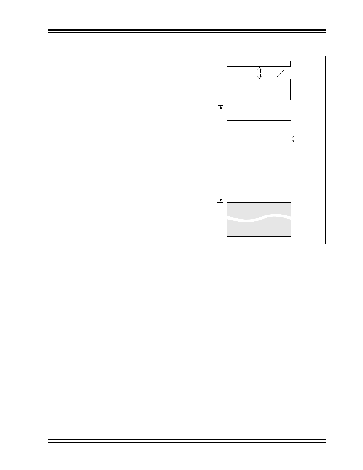
Program Memory Organization
The PIC16FXX has a 13-bit program counter capable
of addressing an 8K x 14 program memory space. For
the PIC16F84A, the first 1K x 14 (0000h-03FFh) are
physically implemented (Figure 2-1). Accessing a loca-
tion above the physically implemented address will
cause a wraparound. For example, for locations 20h,
420h, 820h, C20h, 1020h, 1420h, 1820h, and 1C20h,
the instruction will be the same.
The RESET vector is at 0000h and the interrupt vector
is at 0004h.
FIGURE 2-1:
PROGRAM MEMORY MAP
AND STACK - PIC16F84A
PC<12:0>
Stack Level 1
Stack Level 8
RESET Vector
Peripheral Interrupt Vector
U
s
e
r Me
m
o
ry
Sp
a
c
e
CALL, RETURN
RETFIE, RETLW
13
0000h
0004h
1FFFh
3FFh
PIC16F84A
DS35007C-page 6
2001-2013 Microchip Technology Inc.
2.2
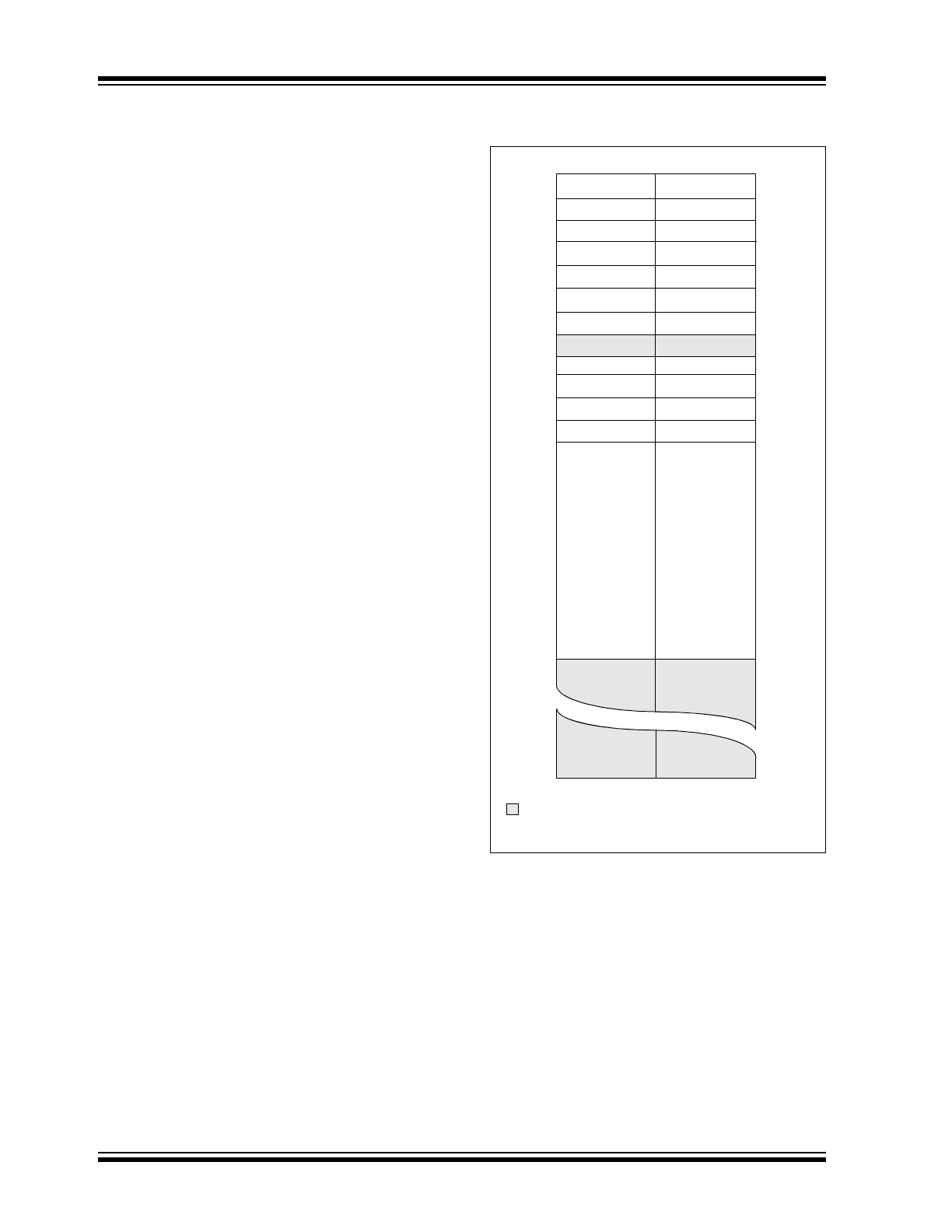
Data Memory Organization
The data memory is partitioned into two areas. The first
is the Special Function Registers (SFR) area, while the
second is the General Purpose Registers (GPR) area.
The SFRs control the operation of the device.
Portions of data memory are banked. This is for both
the SFR area and the GPR area. The GPR area is
banked to allow greater than 116 bytes of general
purpose RAM. The banked areas of the SFR are for the
registers that control the peripheral functions. Banking
requires the use of control bits for bank selection.
These control bits are located in the STATUS Register.
Figure 2-2 shows the data memory map organization.
Instructions MOVWF and MOVF can move values from
the W register to any location in the register file (“F”),
and vice-versa.
The entire data memory can be accessed either
directly using the absolute address of each register file
or indirectly through the File Select Register (FSR)
(Section 2.5). Indirect addressing uses the present
value of the RP0 bit for access into the banked areas of
data memory.
Data memory is partitioned into two banks which
contain the general purpose registers and the special
function registers. Bank 0 is selected by clearing the
RP0 bit (STATUS<5>). Setting the RP0 bit selects Bank
1. Each Bank extends up to 7Fh (128 bytes). The first
twelve locations of each Bank are reserved for the
Special Function Registers. The remainder are Gen-
eral Purpose Registers, implemented as static RAM.
2.2.1
GENERAL PURPOSE REGISTER
FILE
Each General Purpose Register (GPR) is 8-bits wide
and is accessed either directly or indirectly through the
FSR (Section 2.5).
The GPR addresses in Bank 1 are mapped to
addresses in Bank 0. As an example, addressing loca-
tion 0Ch or 8Ch will access the same GPR.
FIGURE 2-2:
REGISTER FILE MAP -
PIC16F84A
File Address
00h
01h
02h
03h
04h
05h
06h
07h
08h
09h
0Ah
0Bh
0Ch
7Fh
80h
81h
82h
83h
84h
85h
86h
87h
88h
89h
8Ah
8Bh
8Ch
FFh
Bank 0
Bank 1
Indirect addr.
(1)
Indirect addr.
(1)
TMR0
OPTION_REG
PCL
STATUS
FSR
PORTA
PORTB
EEDATA
EEADR
PCLATH
INTCON
68
General
Purpose
Registers
(SRAM)
PCL
STATUS
FSR
TRISA
TRISB
EECON1
EECON2
(1)
PCLATH
INTCON
Mapped
in Bank 0
Unimplemented data memory location, read as '0'.
File Address
Note
1: Not a physical register.
CFh
D0h
4Fh
50h
(accesses)
—
—
2001-2013 Microchip Technology Inc.
DS35007C-page 7
PIC16F84A
2.3
Special Function Registers
The Special Function Registers (Figure 2-2 and
Table 2-1) are used by the CPU and Peripheral
functions to control the device operation. These
registers are static RAM.
The special function registers can be classified into two
sets, core and peripheral. Those associated with the
core functions are described in this section. Those
related to the operation of the peripheral features are
described in the section for that specific feature.
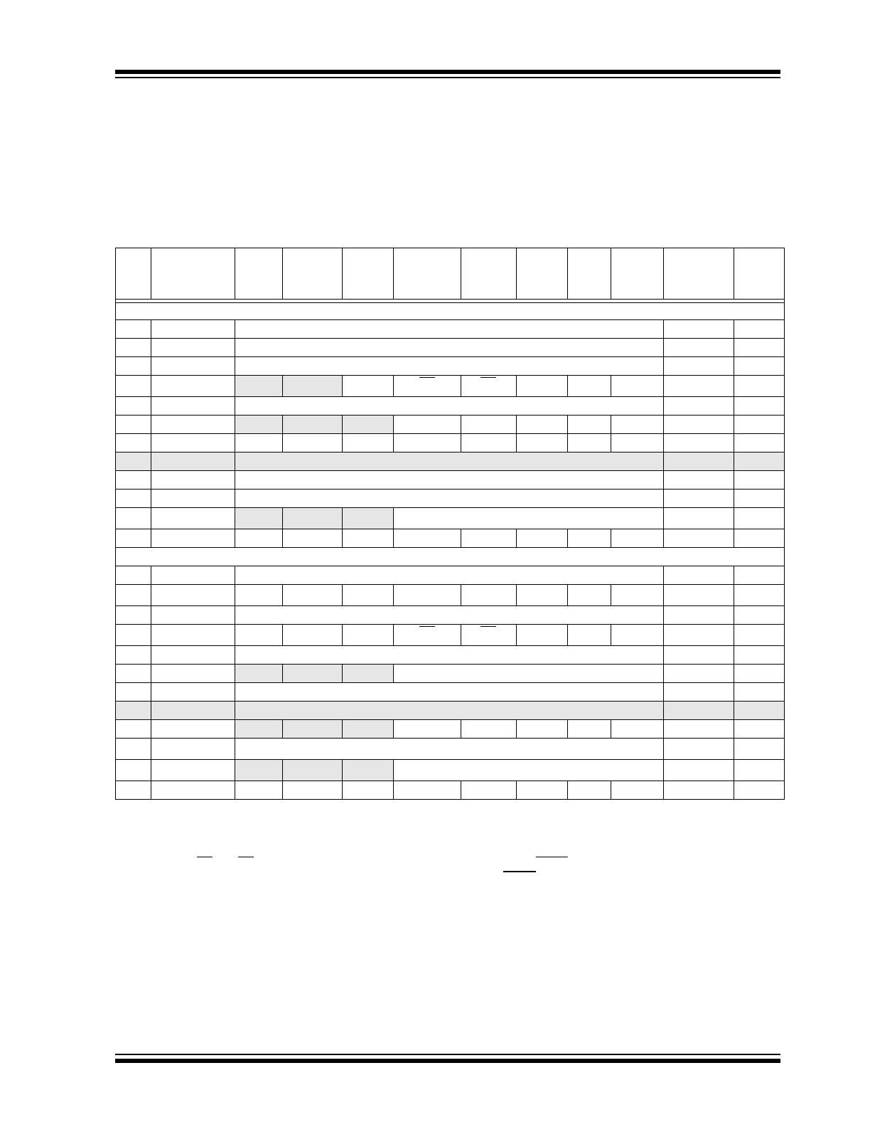
TABLE 2-1:
SPECIAL FUNCTION REGISTER FILE SUMMARY
Addr
Name
Bit 7
Bit 6
Bit 5
Bit 4
Bit 3
Bit 2
Bit 1
Bit 0
Value on
Power-on
RESET
Details
on page
Bank 0
00h
INDF
Uses contents of FSR to address Data Memory (not a physical register)
---- ----
11
01h
TMR0
8-bit Real-Time Clock/Counter
xxxx xxxx
20
02h
PCL
Low Order 8 bits of the Program Counter (PC)
0000 0000
11
03h
STATUS
(2)
IRP
RP1
RP0
TO
PD
Z
DC
C
0001 1xxx
8
04h
FSR
Indirect Data Memory Address Pointer 0
xxxx xxxx
11
05h
PORTA
(4)
—
—
—
RA4/T0CKI
RA3
RA2
RA1
RA0
---x xxxx
16
06h
PORTB
(5)
RB7
RB6
RB5
RB4
RB3
RB2
RB1
RB0/INT xxxx xxxx
18
07h
—
Unimplemented location, read as '0'
—
—
08h
EEDATA
EEPROM Data Register
xxxx xxxx
13,14
09h
EEADR
EEPROM Address Register
xxxx xxxx
13,14
0Ah
PCLATH
—
—
—
Write Buffer for upper 5 bits of the PC
(1)
---0 0000
11
0Bh
INTCON
GIE
EEIE
T0IE
INTE
RBIE
T0IF
INTF
RBIF
0000 000x
10
Bank 1
80h
INDF
Uses Contents of FSR to address Data Memory (not a physical register)
---- ----
11
81h
OPTION_REG
RBPU
INTEDG
T0CS
T0SE
PSA
PS2
PS1
PS0
1111 1111
9
82h
PCL
Low order 8 bits of Program Counter (PC)
0000 0000
11
83h
STATUS
(2)
IRP
RP1
RP0
TO
PD
Z
DC
C
0001 1xxx
8
84h
FSR
Indirect data memory address pointer 0
xxxx xxxx
11
85h
TRISA
—
—
—
PORTA Data Direction Register
---1 1111
16
86h
TRISB
PORTB Data Direction Register
1111 1111
18
87h
—
Unimplemented location, read as '0'
—
—
88h
EECON1
—
—
—
EEIF
WRERR
WREN
WR
RD
---0 x000
13
89h
EECON2
EEPROM Control Register 2 (not a physical register)
---- ----
14
0Ah
PCLATH
—
—
—
Write buffer for upper 5 bits of the PC
(1)
---0 0000
11
0Bh
INTCON
GIE
EEIE
T0IE
INTE
RBIE
T0IF
INTF
RBIF
0000 000x
10
Legend: x = unknown, u = unchanged. - = unimplemented, read as '0', q = value depends on condition
Note
1: The upper byte of the program counter is not directly accessible. PCLATH is a slave register for PC<12:8>. The contents
of PCLATH can be transferred to the upper byte of the program counter, but the contents of PC<12:8> are never trans-
ferred to PCLATH.
2: The TO and PD status bits in the STATUS register are not affected by a MCLR Reset.
3: Other (non power-up) RESETS include: external RESET through MCLR and the Watchdog Timer Reset.
4: On any device RESET, these pins are configured as inputs.
5: This is the value that will be in the port output latch.

PIC16F84A
DS35007C-page 8
2001-2013 Microchip Technology Inc.
2.3.1
STATUS REGISTER
The STATUS register contains the arithmetic status of
the ALU, the RESET status and the bank select bit for
data memory.
As with any register, the STATUS register can be the
destination for any instruction. If the STATUS register is
the destination for an instruction that affects the Z, DC
or C bits, then the write to these three bits is disabled.
These bits are set or cleared according to device logic.
Furthermore, the TO and PD bits are not writable.
Therefore, the result of an instruction with the STATUS
register as destination may be different than intended.
For example, CLRF STATUS will clear the upper three
bits and set the Z bit. This leaves the STATUS register
as 000u u1uu (where u = unchanged).
Only the BCF, BSF, SWAPF and MOVWF instructions
should be used to alter the STATUS register (Table 7-2),
because these instructions do not affect any status bit.
REGISTER 2-1:
STATUS REGISTER (ADDRESS 03h, 83h)
Note 1: The IRP and RP1 bits (STATUS<7:6>)
are not used by the PIC16F84A and
should be programmed as cleared. Use of
these bits as general purpose R/W bits is
NOT recommended, since this may affect
upward compatibility with future products.
2: The C and DC bits operate as a borrow
and digit borrow out bit, respectively, in
subtraction. See the SUBLW and SUBWF
instructions for examples.
3: When the STATUS register is the
destination for an instruction that affects
the Z, DC or C bits, then the write to these
three bits is disabled. The specified bit(s)
will be updated according to device logic
R/W-0
R/W-0
R/W-0
R-1
R-1
R/W-x
R/W-x
R/W-x
IRP
RP1
RP0
TO
PD
Z
DC
C
bit 7
bit 0
bit 7-6
Unimplemented: Maintain as ‘0’
bit 5
RP0: Register Bank Select bits (used for direct addressing)
01
= Bank 1 (80h - FFh)
00
= Bank 0 (00h - 7Fh)
bit 4
TO: Time-out bit
1
= After power-up, CLRWDT instruction, or SLEEP instruction
0
= A WDT time-out occurred
bit 3
PD: Power-down bit
1
= After power-up or by the CLRWDT instruction
0
= By execution of the SLEEP instruction
bit 2
Z: Zero bit
1
= The result of an arithmetic or logic operation is zero
0
= The result of an arithmetic or logic operation is not zero
bit 1
DC: Digit carry/borrow bit (ADDWF, ADDLW,SUBLW,SUBWF instructions) (for borrow, the polarity
is reversed)
1
= A carry-out from the 4th low order bit of the result occurred
0
= No carry-out from the 4th low order bit of the result
bit 0
C: Carry/borrow bit (ADDWF, ADDLW,SUBLW,SUBWF instructions) (for borrow, the polarity is
reversed)
1
= A carry-out from the Most Significant bit of the result occurred
0
= No carry-out from the Most Significant bit of the result occurred
Note:
A subtraction is executed by adding the two’s complement of the second operand.
For rotate (RRF, RLF) instructions, this bit is loaded with either the high or low order
bit of the source register.
Legend:
R = Readable bit
W = Writable bit
U = Unimplemented bit, read as ‘0’
- n = Value at POR
’1’ = Bit is set
’0’ = Bit is cleared
x = Bit is unknown
2001-2013 Microchip Technology Inc.
DS35007C-page 9
PIC16F84A
2.3.2
OPTION REGISTER
The OPTION register is a readable and writable
register which contains various control bits to configure
the TMR0/WDT prescaler, the external INT interrupt,
TMR0, and the weak pull-ups on PORTB.
REGISTER 2-2:
OPTION REGISTER (ADDRESS 81h)
Note:
When the prescaler is assigned to
the WDT (PSA = '1'), TMR0 has a 1:1
prescaler assignment.
R/W-1
R/W-1
R/W-1
R/W-1
R/W-1
R/W-1
R/W-1
R/W-1
RBPU
INTEDG
T0CS
T0SE
PSA
PS2
PS1
PS0
bit 7
bit 0
bit 7
RBPU: PORTB Pull-up Enable bit
1
= PORTB pull-ups are disabled
0
= PORTB pull-ups are enabled by individual port latch values
bit 6
INTEDG: Interrupt Edge Select bit
1
= Interrupt on rising edge of RB0/INT pin
0
= Interrupt on falling edge of RB0/INT pin
bit 5
T0CS: TMR0 Clock Source Select bit
1
= Transition on RA4/T0CKI pin
0
= Internal instruction cycle clock (CLKOUT)
bit 4
T0SE: TMR0 Source Edge Select bit
1
= Increment on high-to-low transition on RA4/T0CKI pin
0
= Increment on low-to-high transition on RA4/T0CKI pin
bit 3
PSA: Prescaler Assignment bit
1
= Prescaler is assigned to the WDT
0
= Prescaler is assigned to the Timer0 module
bit 2-0
PS2:PS0: Prescaler Rate Select bits
Legend:
R = Readable bit
W = Writable bit
U = Unimplemented bit, read as ‘0’
- n = Value at POR
’1’ = Bit is set
’0’ = Bit is cleared
x = Bit is unknown
000
001
010
011
100
101
110
111
1 : 2
1 : 4
1 : 8
1 : 16
1 : 32
1 : 64
1 : 128
1 : 256
1 : 1
1 : 2
1 : 4
1 : 8
1 : 16
1 : 32
1 : 64
1 : 128
Bit Value
TMR0 Rate WDT Rate

PIC16F84A
DS35007C-page 10
2001-2013 Microchip Technology Inc.
2.3.3
INTCON REGISTER
The INTCON register is a readable and writable
register that contains the various enable bits for all
interrupt sources.
REGISTER 2-3:
INTCON REGISTER (ADDRESS 0Bh, 8Bh)
Note:
Interrupt flag bits are set when an interrupt
condition occurs, regardless of the state of
its corresponding enable bit or the global
enable bit, GIE (INTCON<7>).
R/W-0
R/W-0
R/W-0
R/W-0
R/W-0
R/W-0
R/W-0
R/W-x
GIE
EEIE
T0IE
INTE
RBIE
T0IF
INTF
RBIF
bit 7
bit 0
bit 7
GIE: Global Interrupt Enable bit
1
= Enables all unmasked interrupts
0
= Disables all interrupts
bit 6
EEIE: EE Write Complete Interrupt Enable bit
1
= Enables the EE Write Complete interrupts
0
= Disables the EE Write Complete interrupt
bit 5
T0IE: TMR0 Overflow Interrupt Enable bit
1
= Enables the TMR0 interrupt
0
= Disables the TMR0 interrupt
bit 4
INTE: RB0/INT External Interrupt Enable bit
1
= Enables the RB0/INT external interrupt
0
= Disables the RB0/INT external interrupt
bit 3
RBIE: RB Port Change Interrupt Enable bit
1
= Enables the RB port change interrupt
0
= Disables the RB port change interrupt
bit 2
T0IF: TMR0 Overflow Interrupt Flag bit
1
= TMR0 register has overflowed (must be cleared in software)
0
= TMR0 register did not overflow
bit 1
INTF: RB0/INT External Interrupt Flag bit
1
= The RB0/INT external interrupt occurred (must be cleared in software)
0
= The RB0/INT external interrupt did not occur
bit 0
RBIF: RB Port Change Interrupt Flag bit
1
= At least one of the RB7:RB4 pins changed state (must be cleared in software)
0
= None of the RB7:RB4 pins have changed state
Legend:
R = Readable bit
W = Writable bit
U = Unimplemented bit, read as ‘0’
- n = Value at POR
’1’ = Bit is set
’0’ = Bit is cleared
x = Bit is unknown