
2014 Microchip Technology Inc.
DS20005271B-page 1
34AA04
Device Selection Table
Features
• 4 Kbit EEPROM:
- Internally organized as two 256 x 8-bit banks
- Byte or page writes (up to 16 bytes)
- Byte or sequential reads within a single bank
- Self-timed write cycle (5 ms max.)
• JEDEC
®
JC42.4 (EE1004-v) Serial Presence
Detect (SPD) Compliant for DRAM (DDR4)
modules
• High-Speed I
2
C™ Interface:
- Industry standard 1 MHz, 400 kHz, and
100 kHz
- Schmitt Trigger inputs for noise suppression
- SMBus-compatible bus time out
- Cascadable up to eight devices
• Write Protection:
- Reversible software write protection for four
individual 128-byte blocks
• Low-Power CMOS Technology:
- Voltage range: 1.7V to 3.6V
- Write current: 1.5 mA at 3.6V
- Read current: 200 µA at 3.6V, 400 kHz
- Standby current: 1 µA at 3.6V
• High Reliability:
- More than one million erase/write cycles
- Data retention: > 200 years
- ESD protection: > 4000V
• 8-lead PDIP, SOIC, TSSOP, TDFN, and UDFN
Packages
• Available Temperature Ranges:
- Industrial (I): -40°C to +85°C
- Automotive (E): -40°C to +125°C
Description
The Microchip Technology Inc. 34AA04 is a 4 Kbit
Electrically Erasable PROM which utilizes the I
2
C serial
interface and is capable of operation across a broad
voltage range (1.7V to 3.6V). This device is JEDEC
JC42.4 (EE1004-v) Serial Presence Detect (SPD)
compliant and includes reversible software write
protection for each of four independent 128 x 8-bit
blocks. The device features a page write capability of
up to 16 bytes of data. Address pins allow up to eight
devices on the same bus.
The 34AA04 is available in the 8-lead PDIP, SOIC,
TSSOP, TDFN, and UDFN packages.
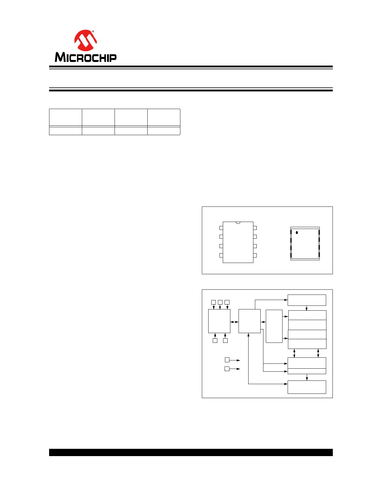
Package Types
Block Diagram
Part
Number
V
CC
Range
Max. Clock
Frequency
Temp
Ranges
34AA04
1.7-3.6
1 MHz
(1)
I, E
Note 1:
400 kHz for 1.8V ≤ V
CC
< 2.2V
100 kHz for V
CC
< 1.8V
A0
A1
A2
V
SS
1
2
3
4
8
7
6
5
V
CC
NC
SCL
SDA
A0
A1
A2
V
SS
NC
SCL
SDA
V
CC
8
7
6
5
1
2
3
4
TDFN/UDFN
PDIP/SOIC/TSSOP
I/O
Control
Logic
Memory
Control
Logic
XDEC
HV Generator
Write-Protect
Circuitry
YDEC
V
CC
V
SS
Sense Amp.
R/W Control
SDA SCL
A0 A1 A2
Block 0
(000h-07Fh)
Block 1
(080h-0FFh)
Block 2
(100h-17Fh)
Block 3
(180h-1FFh)
4K I
2
C
™
Serial EEPROM with Software Write-Protect
34AA04
DS20005271B-page 2
2014 Microchip Technology Inc.
1.0
ELECTRICAL CHARACTERISTICS
Absolute Maximum Ratings
(†)
V
CC
.............................................................................................................................................................................6.5V
All Inputs and Outputs (except A0) w.r.t. V
SS
............................................................................................... -0.3V to 6.5V
A0 Input w.r.t. V
SS
........................................................................................................................................... -0.3 to 12V
Storage Temperature...............................................................................................................................-65°C to +150°C
Ambient Temperature with Power Applied ..............................................................................................-40°C to +125°C
ESD Protection on All Pins
4 kV
† NOTICE:
Stresses above those listed under “Absolute Maximum Ratings” may cause permanent damage to the
device. These are stress ratings only and functional operation of the device at these or any other conditions above
those indicated in the operation sections of the specifications is not implied. Exposure to Absolute Maximum Rating
conditions for extended periods may affect device reliability.
TABLE 1-1:
DC SPECIFICATIONS
DC CHARACTERISTICS
V
CC
= +1.7V to +3.6V
Industrial (I): T
A
= -40°C to +85°C
Automotive (E): T
A
= -40°C to +125°C
Param.
No.
Symbol
Characteristic
Min.
Max.
Units
Conditions
—
A0, A1, A2, SCL, and SDA
—
—
—
D1
V
IH
High-Level Input Voltage
0.7 V
CC
V
CC
+ 0.5
V
D2
V
IL
Low-Level Input Voltage
—
0.3 V
CC
0.2 V
CC
V
V
V
CC
≥ 2.5V
V
CC
< 2.5V
D3
V
HYS
Hysteresis of Schmitt
Trigger Inputs
0.0 V
CC
—
V
(
Note
)
D4
V
OL
Low-Level Output Voltage
—
0.40
0.40
V
V
I
OL
= 20.0 mA, V
CC
= 2.2V
I
OL
= 6.0 mA, V
CC
= 1.7V
D5
V
HV
High-Voltage Detect
(A0 pin only)
7
10
V
V
CC
< 2.2V
V
CC
+ 4.8
10
V
V
CC
2.2V
D6
I
LI
Input Leakage Current
—
±1
A
V
IN
= V
SS
or V
CC
D7
I
LO
Output Leakage Current
—
±1
A
V
OUT
= V
SS
or V
CC
D8
C
IN
, C
OUT
Pin Capacitance
(all inputs/outputs)
—
10
pF
V
CC
= 5.5V (
Note
)
T
A
= 25°C, F
CLK
= 1 MHz
D9
I
CC
write
Operating Current
—
1.5
mA
V
CC
= 3.6V
D10
I
CC
read
—
200
A
V
CC
= 3.6V, SCL = 400 kHz
D11
I
CCS
Standby Current
—
—
1
5
A
A
Industrial
Automotive
SDA, SCL, V
CC
= 3.6V
A0, A1, A2 = V
SS
Note:
This parameter is periodically sampled and not 100% tested.

2014 Microchip Technology Inc.
DS20005271B-page 3
34AA04
TABLE 1-2:
AC SPECIFICATIONS
AC CHARACTERISTICS
V
CC
= +1.7V to +3.6V
Industrial (I): T
A
= -40°C to +85°C
Automotive (E): T
A
= -40°C to +125°C
Param.
No.
Symbol
Characteristic
Min.
Max.
Units
Conditions
1
F
CLK
Clock Frequency (
Note 2
)
10
10
10
100
400
1000
kHz
1.7V
V
CC
< 1.8V
1.8V
V
CC
2.2V
2.2V
V
CC
3.6V
2
T
HIGH
Clock High Time
4000
600
260
—
—
—
ns
1.7V
V
CC
< 1.8V
1.8V
V
CC
2.2V
2.2V
V
CC
3.6V
3
T
LOW
Clock Low Time
4700
1300
500
—
—
—
ns
1.7V
V
CC
< 1.8V
1.8V
V
CC
2.2V
2.2V
V
CC
3.6V
4
T
R
SDA and SCL Rise Time (
Note 1
)
—
—
—
1000
300
120
ns
1.7V
V
CC
< 1.8V
1.8V
V
CC
2.2V
2.2V
V
CC
3.6V
5
T
F
SDA and SCL Fall Time (
Note 1
)
—
—
—
300
300
120
ns
1.7V
V
CC
< 1.8V
1.8V
V
CC
2.2V
2.2V
V
CC
3.6V
6
T
HD
:
STA
Start Condition Hold Time
4000
600
260
—
—
—
ns
1.7V
V
CC
< 1.8V
1.8V
V
CC
2.2V
2.2V
V
CC
3.6V
7
T
SU
:
STA
Start Condition Setup Time
4700
600
260
—
—
—
ns
1.7V
V
CC
< 1.8V
1.8V
V
CC
2.2V
2.2V
V
CC
3.6V
8
T
HD
:
DAT
Data Input Hold Time
0
—
ns
(
Note 3
)
9
T
SU
:
DAT
Data Input Setup Time
250
100
50
—
—
—
ns
1.7V
V
CC
< 1.8V
1.8V
V
CC
2.2V
2.2V
V
CC
3.6V
10
T
SU
:
STO
Stop Condition Setup Time
4000
600
260
—
—
—
ns
1.7V
V
CC
< 1.8V
1.8V
V
CC
2.2V
2.2V
V
CC
3.6V
11
T
AA
Output Valid from Clock (
Note 3
)
200
200
—
3450
900
350
ns
1.7V
V
CC
< 1.8V
1.8V
V
CC
2.2V
2.2V
V
CC
3.6V
12
T
BUF
Bus Free Time: Time the bus must
be free before a new transmission
can start
4700
1300
500
—
—
—
ns
1.7V
V
CC
< 1.8V
1.8V
V
CC
2.2V
2.2V
V
CC
3.6V
13
T
SP
Input Filter Spike Suppression
(SDA and SCL pins)
—
50
ns
(
Note 1
)
14
T
WC
Write Cycle Time (byte or page)
—
5
ms
—
15
T
TIMEOUT
Bus Timeout Time
25
35
ms
—
16
—
Endurance
1M
—
cycles
Page mode, 25°C, V
CC
= 3.6V
(
Note 4
)
Note
1:
Not 100% tested.
2:
The minimum clock frequency of 10 kHz is to prevent the bus timeout from occurring.
3:
As a transmitter, the device must provide an internal minimum delay time to bridge the undefined region (minimum
200 ns) of the falling edge of SCL to avoid unintended generation of Start or Stop conditions.
4:
This parameter is not tested but ensured by characterization. For endurance estimates in a specific application, please
consult the Total Endurance™ Model which can be obtained from Microchip’s web site at www.microchip.com.
34AA04
DS20005271B-page 4
2014 Microchip Technology Inc.
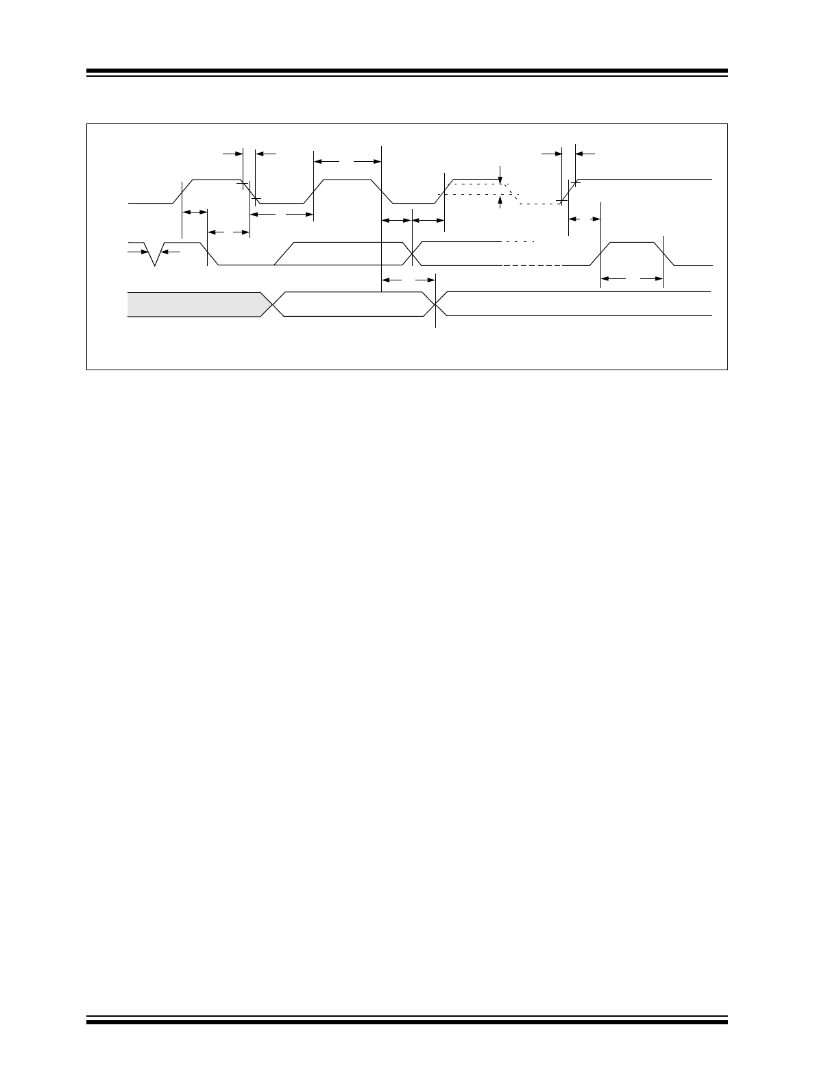
FIGURE 1-1:
BUS TIMING DATA
SCL
SDA
In
SDA
Out
5
7
6
13
3
2
8
9
11
D3
4
10
12
2014 Microchip Technology Inc.
DS20005271B-page 5
34AA04
2.0
PIN DESCRIPTIONS
The descriptions of the pins are listed in
Table 2-1
.
TABLE 2-1:
PIN FUNCTION TABLE
2.1
A0, A1, A2 Chip Address Inputs
The levels on these inputs are compared with the
corresponding bits in the slave address. The chip is
selected if the compare is true.
Up to eight 34AA04 devices may be connected to the
same bus by using different Chip Select bit combina-
tions. These inputs must be connected to either V
SS
or
V
CC
.
The A0 pin also serves as the high-voltage input for
enabling the SWPn and CWP instructions.
2.2
Serial Address/Data Input/Output
(SDA)
This is a bidirectional pin used to transfer addresses
and data into and data out of the device. It is an open
drain terminal. Therefore, the SDA bus requires a pull-
up resistor to V
CC
(typical 10 k
for 100 kHz, 2 k for
400 kHz and 1 MHz).
For normal data transfer, SDA is allowed to change
only during SCL low. Changes during SCL high are
reserved for indicating the Start and Stop conditions.
2.3
Serial Clock (SCL)
This input is used to synchronize the data transfer to
and from the device.
Symbol
PDIP
SOIC
TSSOP
UDFN
TDFN
Description
A0/V
HV
1
1
1
1
1
Chip Address Input, High-Voltage Input
A1
2
2
2
2
2
Chip Address Input
A2
3
3
3
3
3
Chip Address Input
V
SS
4
4
4
4
4
Ground
SDA
5
5
5
5
5
Serial Address/Data I/O
SCL
6
6
6
6
6
Serial Clock
NC
7
7
7
7
7
Not Connected
V
CC
8
8
8
8
8
+1.7V to 3.6V Power Supply
Note:
Exposed pad on TDFN/UDFN can be connected to V
SS
or left floating.
Note:
The comparison between the A0, A1, and
A2 pins and the corresponding Chip
Select bits is disabled for software Write-
Protect and Bank Select commands.

34AA04
DS20005271B-page 6
2014 Microchip Technology Inc.
3.0
FUNCTIONAL DESCRIPTION
The 34AA04 supports a bidirectional 2-wire bus and
data transmission protocol. A device that sends data
onto the bus is defined as a transmitter, and a device
receiving data, as a receiver. The bus has to be
controlled by a master device, which generates the
Serial Clock (SCL), controls the bus access and gener-
ates the Start and Stop conditions, while the 34AA04
works as slave. Both master and slave can operate as
transmitter or receiver, but the master device
determines which mode is activated.
The 4 Kbit array of the 34AA04 is divided into two
separate banks of 2 Kbits each. The 34AA04 also
offers reversible software write protection for each of
four 1 Kbit blocks.
4.0
BUS CHARACTERISTICS
The following bus protocol has been defined:
• Data transfer may be initiated only when the bus
is not busy.
• During data transfer, the data line must remain
stable whenever the clock line is high. Changes in
the data line while the clock line is high will be
interpreted as a Start or Stop condition.
Accordingly, the following bus conditions have been
defined (
Figure 4-1
).
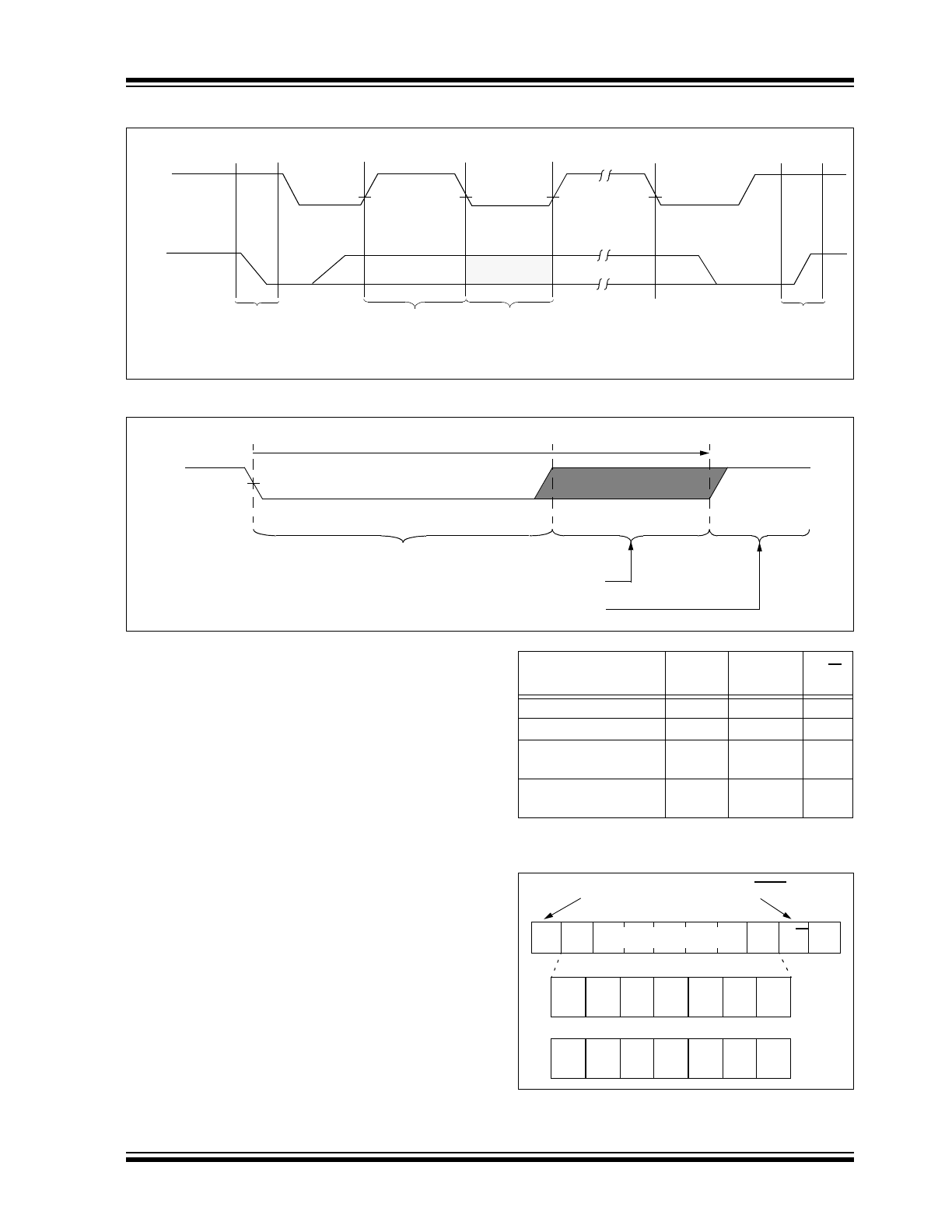
4.1
Bus Not Busy (A)
Both data and clock lines remain high.
4.2
Start Data Transfer (B)
A high-to-low transition of the SDA line while the clock
(SCL) is high determines a Start condition. All
commands must be preceded by a Start condition.
4.3
Stop Data Transfer (C)
A low-to-high transition of the SDA line while the clock
(SCL) is high determines a Stop condition. All
operations must be ended with a Stop condition.
4.4
Data Valid (D)
The state of the data line represents valid data when,
after a Start condition, the data line is stable for the
duration of the high period of the clock signal.
The data on the line must be changed during the low
period of the clock signal. There is one clock pulse per
bit of data.
Each data transfer is initiated with a Start condition and
terminated with a Stop condition. The number of data
bytes transferred between the Start and Stop
conditions is determined by the master device and is,
theoretically, unlimited; although only the last sixteen
will be stored when doing a write operation. When an
overwrite does occur, it will replace data in a first-in,
first-out (FIFO) fashion.
4.5
Acknowledge
Each receiving device, when addressed, is obliged to
generate an Acknowledge after the reception of each
byte. Exceptions to this rule relating to software write
protection are described in
Section 9.0 “Software
Write Protection”
. The master device must generate
an extra clock pulse, which is associated with this
Acknowledge bit.
The device that acknowledges has to pull down the
SDA line during the Acknowledge clock pulse in such a
way that the SDA line is stable low during the high
period of the acknowledge related clock pulse. Of
course, setup and hold times must be taken into
account. During reads, a master must signal an end-of-
data to the slave by not generating an Acknowledge bit
on the last byte that has been clocked out of the slave.
In this case, the slave (34AA04) will leave the data line
high to enable the master to generate the Stop
condition.
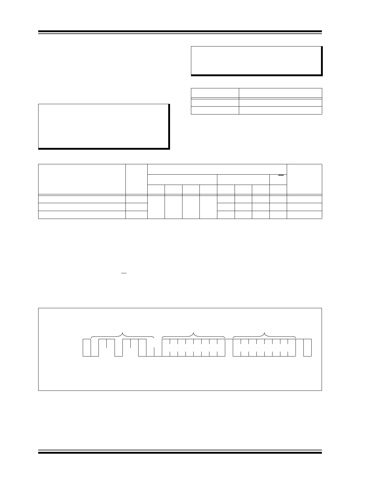
4.6
Bus Timeout
If SCL remains low for the time specified by T
TIMEOUT
,
the 34AA04 will reset the serial interface and ignore all
further communication until another Start condition is
detected (
Figure 4-2
). This dictates the minimum clock
speed as defined by F
CLK
.
Note:
The 34AA04 does not generate any
Acknowledge bits if an internal
programming cycle is in progress.
2014 Microchip Technology Inc.
DS20005271B-page 7
34AA04
FIGURE 4-1:
DATA TRANSFER SEQUENCE ON THE SERIAL BUS
FIGURE 4-2:
BUS TIMEOUT
4.7
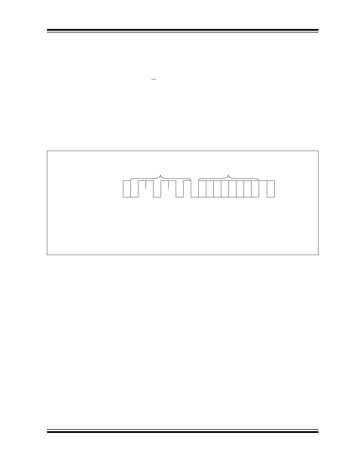
Device Addressing
A control byte is the first byte received following the
Start condition from the master device. The first part of
the control byte consists of a 4-bit control code which is
set to ‘1010’ for normal read and write operations and
‘0110’ for accessing the software write-protect features
and bank selection. The control byte is followed by
three Chip Select bits (A2, A1, A0). The Chip Select bits
allow the use of up to eight 34AA04 devices on the
same bus and are used to determine which device is
accessed. The Chip Select bits in the control byte must
correspond to the logic levels on the corresponding A2,
A1 and A0 pins for the device to respond.
The eighth bit of slave address determines if the master
device wants to read or write to the 34AA04
(
Figure 4-3
). When set to a one, a read operation is
selected. When set to a zero, a write operation is
selected.
FIGURE 4-3:
CONTROL BYTE
ALLOCATION
SCL
SDA
(A)
(B)
(D)
(D)
(A)
(C)
Start
Condition
Address or
Acknowledge
Valid
Data
Allowed
to Change
Stop
Condition
SCL
T
TIMEOUT
(
MIN
)
T
TIMEOUT
(
MAX
)
T
LOW
< T
TIMEOUT
(
MIN
): Bus interface does not reset.
T
TIMEOUT
(
MIN
) < T
LOW
< T
TIMEOUT
(
MAX
): Bus interface may or may not reset.
T
TIMEOUT
(
MAX
) < T
LOW
: Bus interface will reset.
Operation
Control
Code
Chip
Select
R/W
Read
1010
A2 A1 A0
1
Write
1010
A2 A1 A0
0
Read Write-Protect/
Bank Address
0110
A2 A1 A0
1
Set Write-Protect/
Bank Address
0110
A2 A1 A0
0
OR
Start
Read/Write
Slave Address
R/W A
1
0
1
0
A2
A1
A0
0
1
1
0
A2
A1
A0
34AA04
DS20005271B-page 8
2014 Microchip Technology Inc.
5.0
BANK ADDRESSING
To support backwards-compatibility with DDR2/3
(JEDEC EE1002) SPD EEPROMs, the memory array
of the 34AA04 is divided into two separate 256-byte
banks. The Set Bank Address (SBA) commands are
used to set the bank address to either 0 or 1. The
Read Bank Address (RBA) command is used to
determine which bank is currently selected.
TABLE 5-1:
BANK ADDRESS RANGE
TABLE 5-2:
BANK ADDRESSING INSTRUCTION SET
5.1
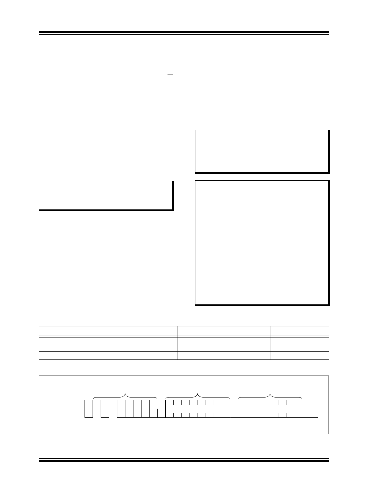
Set Bank Address (SBA)
The Set Bank Address (SBA) commands are used to
select the array bank for future read and write
operations.
The master generates a Start condition followed by the
corresponding control byte for the chosen SBA
command (
Table 5-2
), with the R/W bit set to a logic
‘0’. Note that Chip Select bit A0 of the control byte
effectively determines which bank is selected. The
34AA04 will respond with an Acknowledge, and then
the master transmits two dummy bytes. The 34AA04
will not acknowledge either dummy byte. Finally, the
master generates a Stop condition to end the
operation (
Figure 5-1
).
Array Read and Write commands will operate in the
newly-selected bank until another SBA command is
executed, or the 34AA04 experiences a POR or BOR
event.
FIGURE 5-1:
SET BANK ADDRESS
Note 1:
The bank address is volatile and is reset
to Bank 0 upon power-up.
2:
The comparison between the A0, A1, and
A2 pins and the corresponding Chip
Select bits is disabled for Bank Select
commands.
Note:
Sequential read operations cannot
cross a bank boundary and will roll over
back to the beginning of the selected
bank.
Bank
Logical Array Address
Bank 0
000h-0FFh
Bank 1
100h-1FFh
Function
Abbr
Control Byte
A0 Pin
Control Code
Chip Select Bits
R/W
Bit 7
Bit 6
Bit 5
Bit 4
Bit 3
Bit 2
Bit 1
Bit 0
Set Bank Address to 0
SBA0
0
1
1
0
1
1
0
0
0
, 1, or V
HV
Set Bank Address to 1
SBA1
1
1
1
0
0
, 1, or V
HV
Read Bank Address
RBA
1
1
0
1
0
, 1, or V
HV
S
P
Bus Activity
Master
SDA Line
Bus Activity
S
T
A
R
T
S
T
O
P
Control
Byte
Dummy
Byte
A
C
K
0
1
1 0
0
Dummy
Byte
1
1
A
1
0
N
o
A
C
K
N
o
A
C
K
Note 1:
Chip Select bit A0 specifies which bank to select.
2014 Microchip Technology Inc.
DS20005271B-page 9
34AA04
5.2
Read Bank Address (RBA)
The Read Bank Address (RBA) command allows the
34AA04 to indicate which array bank is currently
selected.
The master generates a Start condition and transmits
the RBA control byte (
Table 5-2
), with the R/W bit set
to logic ‘1’. If Bank 0 is currently selected, the 34AA04
will respond with an Acknowledge signal. If Bank 1 is
currently selected, an Acknowledge will not be
generated. Regardless of the result, the master must
read at least one dummy byte from the 34AA04,
transmitting a Not Acknowledge signal after each byte,
and generate a Stop condition to end the command
(
Figure 5-2
).
FIGURE 5-2:
READ BANK ADDRESS
S
P
Bus Activity
Master
SDA Line
Bus Activity
S
T
O
P
Control
Byte
N
o
A
C
K
S
T
A
R
T
0
1
1
0
1
Dummy
Byte
A
1
C
K
Note 1:
The 34AA04 will only acknowledge if Bank 0 is currently selected.
1
1
0
2:
In accordance with the JEDEC spec, the master is allowed to read multiple dummy bytes,
transmitting a Not Acknowledge after each byte.
34AA04
DS20005271B-page 10
2014 Microchip Technology Inc.
6.0
WRITE OPERATIONS
6.1
Byte Write
Following the Start signal from the master, the control
code (4 bits), the Chip Select bits (3 bits) and the R/W
bit, which is a logic low, are placed onto the bus by the
master transmitter. This indicates to the addressed
slave receiver that the array address byte will follow,
once it has generated an Acknowledge bit during the
ninth clock cycle. Therefore, the next byte transmitted
by the master is the array address and will be written
into the Address Pointer of the 34AA04.
After receiving another Acknowledge signal from the
34AA04, the master device will transmit the data byte to
be written into the addressed memory location. The
34AA04 acknowledges again and the master generates
a Stop condition. This initiates the internal write cycle,
which means that during this time, the 34AA04 will not
generate Acknowledge signals (
Figure 6-1
).
If an attempt is made to write to a software write-pro-
tected portion of the array, the 34AA04 will not acknowl-
edge the data byte, no data will be written, and the
device will immediately accept a new command.
6.2
Page Write
The write control byte, array address and the first data
byte are transmitted to the 34AA04 in the same way as
in a byte write. Instead of generating a Stop condition,
the master transmits up to 15 additional data bytes to
the 34AA04, which are temporarily stored in the on-
chip page buffer and will be written into the memory
after the master has transmitted a Stop condition. Upon
receipt of each word, the four lower order Address
Pointer bits are internally incremented by one. The
higher order four bits of the array address, as well as
the bank selection, remain constant. If the master
should transmit more than 16 bytes prior to generating
the Stop condition, the address counter will roll over
and the previously received data will be overwritten. As
with the byte write operation, once the Stop condition is
received, an internal write cycle will begin (
Figure 6-2
).
If an attempt is made to write to a software write-pro-
tected portion of the array, the 34AA04 will not
acknowledge the data byte, no data will be written, and
the device will immediately accept a new command.
TABLE 6-1:
DEVICE RESPONSE WHEN WRITING DATA
FIGURE 6-1:
BYTE WRITE
Note:
It is recommended to perform a Set Bank
Address command before initiating a
Write command to ensure the desired
bank is selected.
Note:
When doing a write of less than 16 bytes,
the data in the rest of the page is
refreshed along with the data bytes being
written. This will force the entire page to
endure a write cycle. For this reason,
endurance is specified per page.
Note:
Page write operations are limited to
writing bytes within a single physical page,
regardless of the number of bytes actually
being written. Physical page boundaries
start at addresses that are integer multi-
ples of the page buffer size (or ‘page size’)
and end at addresses that are integer mul-
tiples of [page size – 1]. If a Page Write
command attempts to write across a phys-
ical page boundary, the result is that the
data wraps around to the beginning of the
current page (overwriting data previously
stored there), instead of being written to
the next page, as might be expected. It is,
therefore, necessary for the application
software to prevent page write operations
that would attempt to cross a page
boundary.
Status
Command
ACK
Address
ACK
Data Byte
ACK
Write Cycle
Protected with SWPn
Page or Byte Write in
Protected Block
ACK
Address
ACK
Data
NoACK
No
Not Protected
Page or Byte Write
ACK
Address
ACK
Data
ACK
Yes
S
P
Bus Activity
Master
SDA Line
Bus Activity
S
T
A
R
T
S
T
O
P
Control
Byte
Array
Address
Data
A
C
K
A
C
K
A
C
K