
1998-2013 Microchip Technology Inc.
DS30605D-page 1
PIC16C63A/65B/73B/74B
Devices included in this data sheet:
PIC16CXX Microcontroller Core Features:
• High performance RISC CPU
• Only 35 single word instructions to learn
• All single cycle instructions except for program
branches which are two cycle
• Operating speed: DC - 20 MHz clock input
DC - 200 ns instruction cycle
• 4 K x 14 words of Program Memory,
192 x 8 bytes of Data Memory (RAM)
• Interrupt capability
• Eight-level deep hardware stack
• Direct, indirect and relative addressing modes
• Power-on Reset (POR)
• Power-up Timer (PWRT) and Oscillator Start-up
Timer (OST)
• Watchdog Timer (WDT) with its own on-chip RC
oscillator for reliable operation
• Programmable code protection
• Power-saving SLEEP mode
• Selectable oscillator options
• Low power, high speed CMOS EPROM
technology
• Wide operating voltage range: 2.5V to 5.5V
• High Sink/Source Current 25/25 mA
• Commercial, Industrial and Automotive
temperature ranges
• Low power consumption:
- < 5 mA @ 5V, 4 MHz
- 23
A typical @ 3V, 32 kHz
- < 1.2
A typical standby current
PIC16C7X Peripheral Features:
• Timer0: 8-bit timer/counter with 8-bit prescaler
• Timer1: 16-bit timer/counter with prescaler
can be incremented during SLEEP via external
crystal/clock
• Timer2: 8-bit timer/counter with 8-bit period
register, prescaler and postscaler
• Capture, Compare, PWM modules
- Capture is 16-bit, max. resolution is 200 ns
- Compare is 16-bit, max. resolution is 200 ns
- PWM max. resolution is 10-bit
• 8-bit multichannel Analog-to-Digital converter
• Synchronous Serial Port (SSP) with SPI
TM
and I
2
C
TM
• Universal Synchronous Asynchronous Receiver
Transmitter (USART/SCI)
• Parallel Slave Port (PSP), 8-bits wide with
external RD, WR and CS controls
• Brown-out detection circuitry for Brown-out Reset
(BOR)
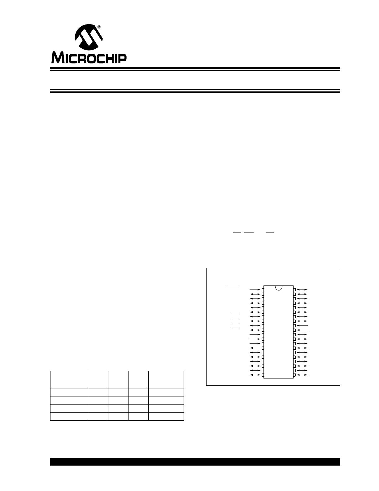
Pin Diagram:
• PIC16C63A
• PIC16C73B
• PIC16C65B
• PIC16C74B
Devices
I/O
Pins
A/D
Chan.
PSP
Interrupts
PIC16C63A
22
-
No
10
PIC16C65B
33
-
Yes
11
PIC16C73B
22
5
No
11
PIC16C74B
33
8
Yes
12
PDIP, Windowed CERDIP
RB7
RB6
RB5
RB4
RB3
RB2
RB1
RB0/INT
V
DD
V
SS
RD7/PSP7
RD6/PSP6
RD5/PSP5
RD4/PSP4
RC7/RX/DT
RC6/TX/CK
RC5/SDO
RC4/SDI/SDA
RD3/PSP3
RD2/PSP2
MCLR/V
PP
RA0/AN0
RA1/AN1
RA2/AN2
RA3/AN3/V
REF
RA4/T0CKI
RA5/SS/AN4
RE0/RD/AN5
RE1/WR/AN6
RE2/CS/AN7
V
DD
V
SS
OSC1/CLKIN
OSC2/CLKOUT
RC0/T1OSO/T1CKI
RC1/T1OSI/CCP2
RC2/CCP1
RC3/SCK/SCL
RD0/PSP0
RD1/PSP1
1
2
3
4
5
6
7
8
9
10
11
12
13
14
15
16
17
18
19
20
40
39
38
37
36
35
34
33
32
31
30
29
28
27
26
25
24
23
22
21
PIC
16C
6
5
B
PIC
1
6C
74
B
8-Bit CMOS Microcontrollers with A/D Converter
PIC16C63A/65B/73B/74B
DS30605D-page 2
1998-2013 Microchip Technology Inc.
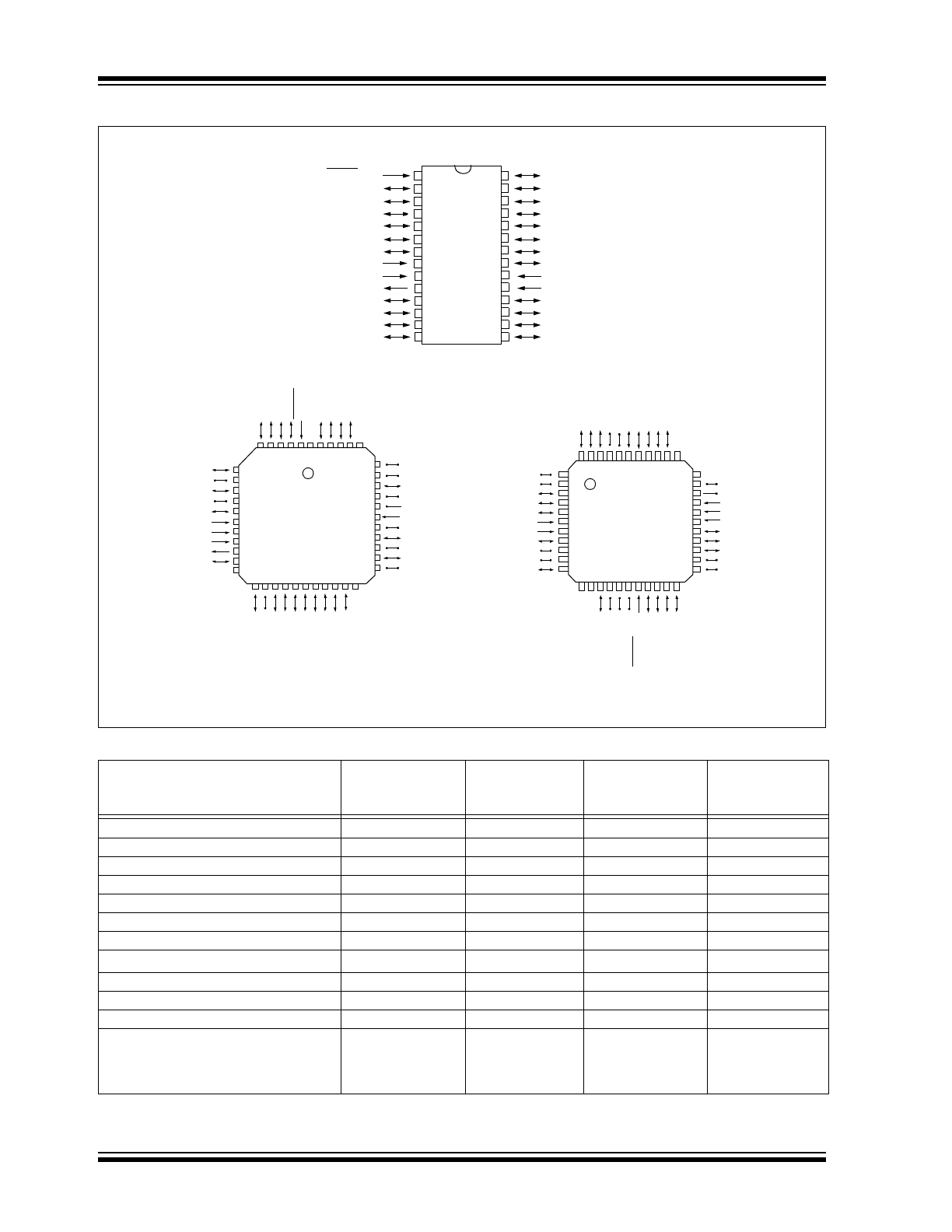
MCLR/V
PP
RA0/AN0
RA1/AN1
RA2/AN2
RA3/AN3/V
REF
RA4/T0CKI
RA5/SS/AN4
V
SS
OSC1/CLKIN
OSC2/CLKOUT
RC0/T1OSO/T1CKI
RC1/T1OSI/CCP2
RC2/CCP1
RC3/SCK/SCL
RB7
RB6
RB5
RB4
RB3
RB2
RB1
RB0/INT
V
DD
V
SS
RC7/RX/DT
RC6/TX/CK
RC5/SDO
RC4/SDI/SDA
• 1
2
3
4
5
6
7
8
9
10
11
12
13
14
28
27
26
25
24
23
22
21
20
19
18
17
16
15
SDIP, SOIC, Windowed CERDIP
RB3
RB2
RB1
RB0/INT
V
DD
V
SS
RD7/PSP7
RD6/PSP6
RD5/PSP5
RD4/PSP4
RC7/RX/DT
RA4/T0CKI
RA5/SS/AN4
RE0/RD/AN5
RE1/WR/AN6
RE2/CS/AN7
V
DD
V
SS
OSC1/CLKIN
OSC2/CLKOUT
RC0/T1OSO/T1CKI
NC
RA3
/AN3
/V
RE
F
RA2
/AN2
RA1
/AN1
RA0
/AN0
MC
L
R
/V
PP
NC RB7 RB6 RB5 RB4 NC
7
8
9
10
11
12
13
14
15
16
17
39
38
37
36
35
34
33
32
31
30
29
NC
RC6
/T
X/CK
RC
5
/SDO
RC4
/SDI/
S
DA
RD3
/PSP3
RD2
/PSP2
RD1
/PSP1
RD0
/PSP0
RC
3
/SCK/
SCL
RC2
/CCP1
6
5
4
3
2
1
44
43
42
41
40
28
27
26
25
24
23
22
21
20
19
18
PIC16C65B
NC
RC0/T1OSO/T1CKI
OSC2/CLKOUT
OSC1/CLKIN
V
SS
V
DD
RE2/CS/AN7
RE1/WR/AN6
RE0/RD/AN5
RA5/SS/AN4
RA4/T0CKI
RC7/RX/DT
RD4/PSP4
RD5/PSP5
RD6/PSP6
RD7/PSP7
V
SS
V
DD
RB0/INT
RB1
RB2
RB3
RC6
/T
X/CK
RC5
/SDO
RC4
/SDI/SDA
RD3
/PSP3
RD2
/PSP2
RD1
/PSP1
RD0
/PSP0
RC3
/SCK/SCL
RC2
/CCP1
RC1
/T
1
O
SI
/CCP2
NC
1
2
3
4
5
6
7
8
9
10
11
33
32
31
30
29
28
27
26
25
24
23
RA3
/AN3
/V
RE
F
RA
2
/AN2
RA
1
/AN1
RA
0
/AN0
MC
L
R
/V
PP
RB7
RB6
RB5
RB4
NC
NC
44
43
42
41
40
39
38
37
36
35
34
22
21
20
19
18
17
16
15
14
13
12
MQFP
PLCC
PIC16C74B
TQFP
RC1
/T
1
O
SI/CCP2
PIC16C65B
PIC16C74B
PIC1
6C63
A
PIC16C7
3
B
Key Features
PIC
®
Mid-Range MCU Family Reference
Manual (DS33023)
PIC16C63A
PIC16C65B
PIC16C73B
PIC16C74B
Program Memory (EPROM) x 14
4 K
4 K
4 K
4 K
Data Memory (Bytes) x 8
192
192
192
192
Pins
28
40
28
40
Parallel Slave Port
—
Yes
—
Yes
Capture/Compare/PWM Modules
2
2
2
2
Timer Modules
3
3
3
3
A/D Channels
—
—
5
8
Serial Communication
SPI/I
2
C, USART
SPI/I
2
C, USART
SPI/I
2
C, USART
SPI/I
2
C, USART
In-Circuit Serial Programming
Yes
Yes
Yes
Yes
Brown-out Reset
Yes
Yes
Yes
Yes
Interrupt Sources
10
11
11
12
Packages
28-pin SDIP, SOIC,
SSOP,
Windowed CERDIP
40-pin PDIP;
44-pin PLCC,
MQFP, TQFP,
Windowed CERDIP
28-pin SDIP, SOIC,
SSOP,
Windowed CERDIP
40-pin PDIP;
44-pin PLCC,
MQFP, TQFP,
Windowed CERDIP

1998-2013 Microchip Technology Inc.
DS30605D-page 3
PIC16C63A/65B/73B/74B
Table of Contents
1.0
General Description...................................................................................................................................................................... 5
2.0
PIC16C63A/65B/73B/74B Device Varieties ................................................................................................................................. 7
3.0
Architectural Overview ................................................................................................................................................................. 9
4.0
Memory Organization ................................................................................................................................................................. 15
5.0
I/O Ports ..................................................................................................................................................................................... 29
6.0
Timer0 Module ........................................................................................................................................................................... 39
7.0
Timer1 Module ........................................................................................................................................................................... 43
8.0
Timer2 Module ........................................................................................................................................................................... 47
9.0
Capture/Compare/PWM Modules .............................................................................................................................................. 49
10.0 Synchronous Serial Port (SSP) Module ..................................................................................................................................... 55
11.0 Addressable Universal Synchronous Asynchronous Receiver Transmitter (USART)................................................................ 65
12.0 Analog-to-Digital Converter (A/D) Module ................................................................................................................................. 79
13.0 Special Features of the CPU...................................................................................................................................................... 85
14.0 Instruction Set Summary ............................................................................................................................................................ 99
15.0 Development Support............................................................................................................................................................... 107
16.0 Electrical Characteristics .......................................................................................................................................................... 113
17.0 DC and AC Characteristics Graphs and Tables....................................................................................................................... 139
18.0 Packaging Information.............................................................................................................................................................. 153
Appendix A:
Revision History ........................................................................................................................................................ 165
Appendix B:
Device Differences..................................................................................................................................................... 165
Appendix C:
Device Migrations - PIC16C63/65A/73A/74A
PIC16C63A/65B/73B/74B ............................................................. 166
Appendix D:
Migration from Baseline to Mid-Range Devices......................................................................................................... 168
On-Line Support................................................................................................................................................................................. 175
Reader Response .............................................................................................................................................................................. 176
Product Identification System ............................................................................................................................................................ 177
TO OUR VALUED CUSTOMERS
It is our intention to provide our valued customers with the best documentation possible to ensure successful use of your Microchip
products. To this end, we will continue to improve our publications to better suit your needs. Our publications will be refined and
enhanced as new volumes and updates are introduced.
If you have any questions or comments regarding this publication, please contact the Marketing Communications Department via
E-mail at docerrors@mail.microchip.com or fax the Reader Response Form in the back of this data sheet to (480) 792-4150.
We welcome your feedback.
Most Current Data Sheet
To obtain the most up-to-date version of this data sheet, please register at our Worldwide Web site at:
http://www.microchip.com
You can determine the version of a data sheet by examining its literature number found on the bottom outside corner of any page.
The last character of the literature number is the version number, (e.g., DS30000A is version A of document DS30000).
Errata
An errata sheet, describing minor operational differences from the data sheet and recommended workarounds, may exist for current
devices. As device/documentation issues become known to us, we will publish an errata sheet. The errata will specify the revision
of silicon and revision of document to which it applies.
To determine if an errata sheet exists for a particular device, please check with one of the following:
• Microchip’s Worldwide Web site; http://www.microchip.com
• Your local Microchip sales office (see last page)
• The Microchip Corporate Literature Center; U.S. FAX: (480) 792-7277
When contacting a sales office or the literature center, please specify which device, revision of silicon and data sheet (include liter-
ature number) you are using.
Customer Notification System
Register on our web site at www.microchip.com/cn to receive the most current information on all of our products.

PIC16C63A/65B/73B/74B
DS30605D-page 4
1998-2013 Microchip Technology Inc.
NOTES:

1998-2013 Microchip Technology Inc.
DS30605D-page 5
PIC16C63A/65B/73B/74B
1.0
GENERAL DESCRIPTION
The PIC16C63A/65B/73B/74B devices are
low cost,
high performance, CMOS, fully-static, 8-bit micro-
controllers in the PIC16CXX mid-range family.
All PIC
®
microcontrollers employ an advanced RISC
architecture. The PIC16CXX microcontroller family has
enhanced core features, eight-level deep stack and
multiple internal and external interrupt sources. The
separate instruction and data buses of the Harvard
architecture allow a 14-bit wide instruction word with
the separate 8-bit wide data. The two stage instruction
pipeline allows all instructions to execute in a single
cycle, except for program branches, which require two
cycles. A total of 35 instructions (reduced instruction
set) are available. Additionally, a large register set
gives some of the architectural innovations used to
achieve a very high performance.
The PIC16C63A/73B devices have 22 I/O pins. The
PIC16C65B/74B devices have 33 I/O pins. Each
device has 192 bytes of RAM. In addition, several
peripheral features are available, including: three timer/
counters, two Capture/Compare/PWM modules, and
two serial ports. The Synchronous Serial Port (SSP)
can be configured as either a 3-wire Serial Peripheral
Interface (SPI) or the two-wire Inter-Integrated Circuit
(I
2
C) bus. The Universal Synchronous Asynchronous
Receiver Transmitter (USART) is also known as the
Serial Communications Interface or SCI. Also, a 5-
channel high speed 8-bit A/D is provided on the
PIC16C73B, while the PIC16C74B offers 8 channels.
The 8-bit resolution is ideally suited for applications
requiring low cost analog interface, e.g., thermostat
control, pressure sensing, etc.
The PIC16C63A/65B/73B/74B devices have special
features to reduce external components, thus reducing
cost, enhancing system reliability and reducing power
consumption. There are four oscillator options, of which
the single pin RC oscillator provides a low cost solution,
the LP oscillator minimizes power consumption, XT is
a standard crystal, and the HS is for high speed crys-
tals. The SLEEP (power-down) feature provides a
power-saving mode. The user can wake-up the chip
from SLEEP through several external and internal
interrupts and RESETS.
A highly reliable Watchdog Timer (WDT), with its own
on-chip RC oscillator, provides protection against soft-
ware lockup, and also provides one way of waking the
device from SLEEP.
A UV erasable CERDIP packaged version is ideal for
code development, while the cost effective One-Time-
Programmable (OTP) version is suitable for production
in any volume.
The PIC16C63A/65B/73B/74B devices fit nicely in
many applications ranging from security and remote
sensors to appliance control and automotive. The
EPROM technology makes customization of applica-
tion programs (transmitter codes, motor speeds,
receiver frequencies, etc.) extremely fast and con-
venient. The small footprint packages make this micro-
controller series perfect for all applications with space
limitations. Low cost, low power, high performance,
ease of use and I/O flexibility make the PIC16C63A/
65B/73B/74B devices very versatile, even in areas
where no microcontroller use has been considered
before (e.g., timer functions, serial communication,
capture and compare, PWM functions and coprocessor
applications).
1.1
Family and Upward Compatibility
Users familiar with the PIC16C5X microcontroller fam-
ily will realize that this is an enhanced version of the
PIC16C5X architecture. Please refer to Appendix A for
a detailed list of enhancements. Code written for the
PIC16C5X can be easily ported to the PIC16CXX fam-
ily of devices (Appendix B).
1.2
Development Support
PIC
®
devices are supported by the complete line of
Microchip Development tools.
Please refer to Section 15.0 for more details about
Microchip’s development tools.

PIC16C63A/65B/73B/74B
DS30605D-page 6
1998-2013 Microchip Technology Inc.
NOTES:

1998-2013 Microchip Technology Inc.
DS30605D-page 7
PIC16C63A/65B/73B/74B
2.0
PIC16C63A/65B/73B/74B
DEVICE
VARIETIES
A variety of frequency ranges and packaging options
are available. Depending on application and production
requirements, the proper device option can be selected
using the information in the PIC16C63A/65B/73B/74B
Product Identification System section at the end of this
data sheet. When placing orders, please use that page
of the data sheet to specify the correct part number.
For the PIC16C7X family, there are two device “types”
as indicated in the device number:
1.
C, as in PIC16C74. These devices have
EPROM type memory and operate over the
standard voltage range.
2.
LC, as in PIC16LC74. These devices have
EPROM type memory and operate over an
extended voltage range.
2.1
UV Erasable Devices
The UV erasable version, offered in windowed CERDIP
packages, is optimal for prototype development and
pilot programs. This version can be erased and
reprogrammed to any of the oscillator modes.
Microchip's PICSTART
Plus and PRO MATE
II
programmers both support programming of the
PIC16C63A/65B/73B/74B.
2.2
One-Time-Programmable (OTP)
Devices
The availability of OTP devices is especially useful for
customers who need the flexibility for frequent code
updates and small volume applications.
The OTP devices, packaged in plastic packages, per-
mit the user to program them once. In addition to the
program memory, the configuration bits must also be
programmed.
2.3
Quick-Turnaround-Production
(QTP) Devices
Microchip offers a QTP Programming Service for fac-
tory production orders. This service is made available
for users who choose not to program a medium to high
quantity of units and whose code patterns have stabi-
lized. The devices are identical to the OTP devices but
with all EPROM locations and configuration options
already programmed by the factory. Certain code and
prototype verification procedures apply before produc-
tion shipments are available. Please contact your local
Microchip Technology sales office for more details.
2.4
Serialized Quick-Turnaround
Production (SQTP
SM
) Devices
Microchip offers a unique programming service where
a few user-defined locations in each device are pro-
grammed with different serial numbers. The serial num-
bers may be random, pseudo-random or sequential.
Serial programming allows each device to have a
unique number, which can serve as an entry code,
password or ID number.

PIC16C63A/65B/73B/74B
DS30605D-page 8
1998-2013 Microchip Technology Inc.
NOTES:

1998-2013 Microchip Technology Inc.
DS30605D-page 9
PIC16C63A/65B/73B/74B
3.0
ARCHITECTURAL OVERVIEW
The high performance of the PIC16CXX family can be
attributed to a number of architectural features com-
monly found in RISC microprocessors. To begin with,
the PIC16CXX uses a Harvard architecture, in which
program and data are accessed from separate memo-
ries using separate buses. This improves bandwidth
over traditional von Neumann architecture, in which
program and data are fetched from the same memory
using the same bus. Separating program and data
buses further allows instructions to be sized differently
than the 8-bit wide data word. Instruction opcodes are
14-bits wide, making it possible to have all single word
instructions. A 14-bit wide program memory access
bus fetches a 14-bit instruction in a single cycle. A
two-stage pipeline overlaps fetch and execution of
instructions (Example 3-1). Consequently, most
instructions execute in a single cycle (200 ns @
20 MHz) except for program branches.
All devices covered by this data sheet contain
4K x 14-bit program memory and 192 x 8-bit data
memory.
The PIC16CXX can directly, or indirectly, address its
register files or data memory. All Special Function Reg-
isters, including the program counter, are mapped in
the data memory. The PIC16CXX has an orthogonal
(symmetrical) instruction set that makes it possible to
carry out any operation on any register using any
addressing mode. This symmetrical nature and lack of
‘special optimal situations’ make programming with the
PIC16CXX simple yet efficient. In addition, the learning
curve is reduced significantly.
PIC16CXX devices contain an 8-bit ALU and working
register. The ALU is a general purpose arithmetic unit.
It performs arithmetic and Boolean functions between
the data in the working register and any register file.
The ALU is 8-bits wide and capable of addition, sub-
traction, shift and logical operations. Unless otherwise
mentioned, arithmetic operations are two's comple-
ment in nature. In two-operand instructions, typically
one operand is the working register (W register). The
other operand is a file register or an immediate con-
stant. In single operand instructions, the operand is
either the W register or a file register.
The W register is an 8-bit working register used for ALU
operations. It is not an addressable register.
Depending on the instruction executed, the ALU may
affect the values of the Carry (C), Digit Carry (DC), and
Zero (Z) bits in the STATUS register. The C and DC bits
operate as a borrow bit and a digit borrow out bit,
respectively, in subtraction. See the SUBLW and SUBWF
instructions for examples.
PIC16C63A/65B/73B/74B
DS30605D-page 10
1998-2013 Microchip Technology Inc.
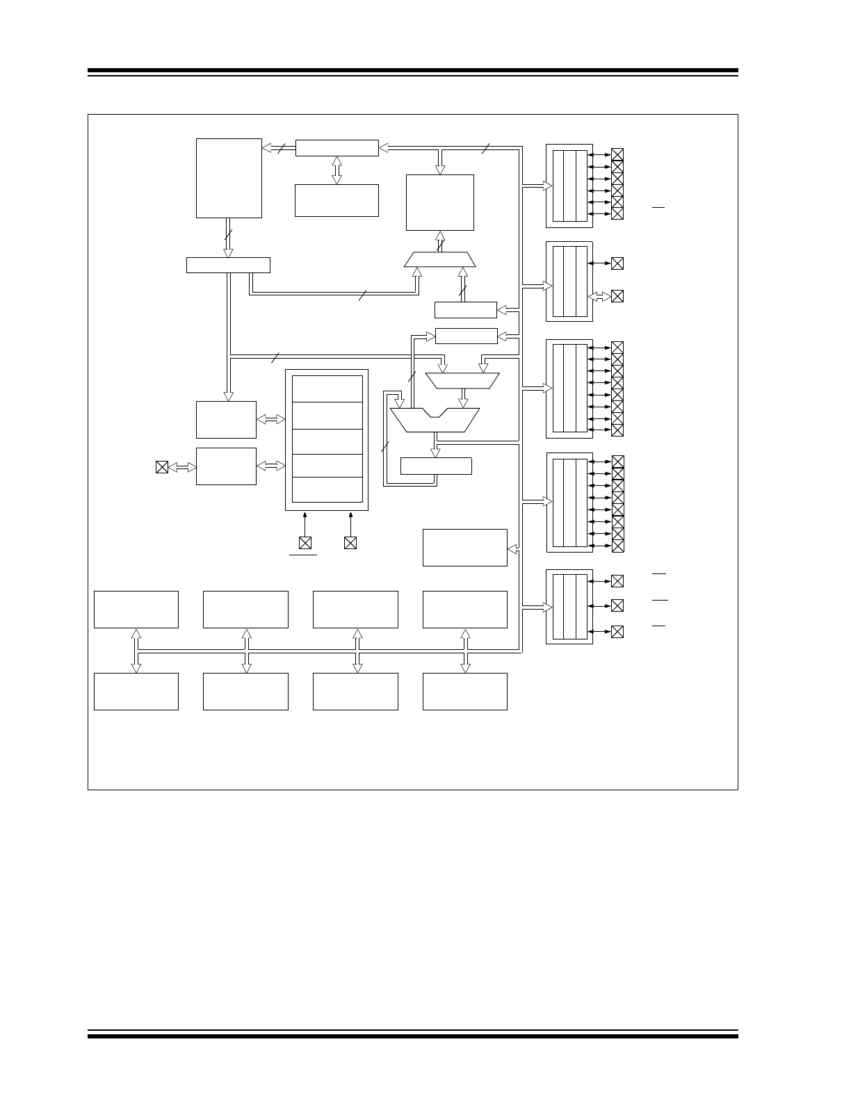
FIGURE 3-1:
PIC16C63A/65B/73B/74B BLOCK DIAGRAM
EPROM
Program
Memory
13
Data Bus
8
14
Program
Bus
Instruction reg
Program Counter
8 Level Stack
(13-bit)
RAM
File
Registers
Direct Addr
7
RAM Addr
(1)
9
Addr MUX
Indirect
Addr
FSR reg
STATUS reg
MUX
ALU
W reg
Power-up
Timer
Oscillator
Start-up Timer
Power-on
Reset
Watchdog
Timer
Instruction
Decode &
Control
Timing
Generation
OSC1/CLKIN
OSC2/CLKOUT
MCLR
V
DD
, V
SS
PORTA
PORTB
PORTC
PORTD
(3)
PORTE
(3)
RA4/T0CKI
RA5/SS/AN4
(2)
RB0/INT
RB7:RB1
RC0/T1OSO/T1CKI
RC1/T1OSI/CCP2
RC2/CCP1
RC3/SCK/SCL
RC4/SDI/SDA
RC5/SDO
RC6/TX/CK
RC7/RX/DT
RD6/PSP6
RE0/RD/AN5
(2,3)
RE1/WR/AN6
(2,3)
RE2/CS/AN7
(2,3)
8
8
Brown-out
Reset
Note
1: Higher order bits are from the STATUS register.
2: A/D is not available on the PIC16C63A/65B.
3: PSP and Ports D and E are not available on PIC16C63A/73B.
USART
CCP1
CCP2
Synchronous
A/D
(2)
Timer0
Timer1
Timer2
Serial Port
RA3/AN3/V
REF
(2)
RA2/AN2
(2)
RA1/AN1
(2)
RA0/AN0
(2)
Parallel Slave Port
8
3
(3)
RD1/PSP1
RD2/PSP2
RD3/PSP3
RD4/PSP4
RD5/PSP5
RD0/PSP0
RD7/PSP7