
© 2008 Microchip Technology Inc.
DS22058C-page 1
MCP6V01/2/3
Features
• High DC Precision:
- V
OS
Drift: ±50 nV/°C (maximum)
- V
OS
: ±2 µV (maximum)
- A
OL
: 130 dB (minimum)
- PSRR: 130 dB (minimum)
- CMRR: 130 dB (minimum)
- E
ni
: 2.5 µV
P-P
(typical), f = 0.1 Hz to 10 Hz
- E
ni
: 0.79 µVp-p (typical), f = 0.01 Hz to 1 Hz
• Low Power and Supply Voltages:
- I
Q
: 300 µA/amplifier (typical)
- Wide Supply Voltage Range: 1.8V to 5.5V
• Easy to Use:
- Rail-to-Rail Input/Output
- Gain Bandwidth Product: 1.3 MHz (typical)
- Unity Gain Stable
- Available in Single and Dual
- Single with Chip Select (CS): MCP6V03
• Extended Temperature Range: -40°C to +125°C
Typical Applications
• Portable Instrumentation
• Sensor Conditioning
• Temperature Measurement
• DC Offset Correction
• Medical Instrumentation
Design Aids
• SPICE Macro Models
• FilterLab
®
Software
• Mindi™ Circuit Designer & Simulator
• Microchip Advanced Part Selector (MAPS)
• Analog Demonstration and Evaluation Boards
• Application Notes
Related Parts
• MCP6V06/7/8: Non-spread clock, lower noise
Description
The Microchip Technology Inc. MCP6V01/2/3 family of
operational amplifiers has input offset voltage
correction for very low offset and offset drift. These
devices have a wide gain bandwidth product (1.3 MHz,
typical) and strongly reject switching noise. They are
unity gain stable, have no 1/f noise, and have good
PSRR and CMRR. These products operate with a
single supply voltage as low as 1.8V, while drawing
300 µA/amplifier (typical) of quiescent current.
The Microchip Technology Inc. MCP6V01/2/3 op amps
are offered in single (MCP6V01), single with Chip
Select (CS) (MCP6V03), and dual (MCP6V02). They
are designed in an advanced CMOS process.
Package Types (top view)
V
IN
+
V
IN
–
V
SS
V
DD
V
OUT
1
2
3
4
8
7
6
5 NC
NC
NC
V
INA
+
V
INA
–
V
SS
1
2
3
4
8
7
6
5
V
OUTA
V
DD
V
OUTB
V
INB
–
V
INB
+
MCP6V01
SOIC
MCP6V02
SOIC
V
IN
+
V
IN
–
V
SS
V
DD
V
OUT
1
2
3
4
8
7
6
5 NC
CS
NC
MCP6V03
SOIC
MCP6V01
2x3 TDFN *
V
IN
+
V
IN
–
V
SS
V
DD
V
OUT
1
2
3
4
8
7
6
5 NC
NC
NC
* Includes Exposed Thermal Pad (EP); see
Table 3-1
.
EP
9
MCP6V02
4x4 DFN *
V
INA
+
V
INA
–
V
SS
V
OUTB
V
INB
–
1
2
3
4
8
7
6
5 V
INB
+
V
DD
V
OUTA
EP
9
MCP6V03
2x3 TDFN *
V
IN
+
V
IN
–
V
SS
V
DD
V
OUT
1
2
3
4
8
7
6
5 NC
CS
NC
EP
9
300 µA, Auto-Zeroed Op Amps
MCP6V01/2/3
DS22058C-page 2
© 2008 Microchip Technology Inc.
Typical Application Circuit
Offset Voltage Correction for Power Driver
MCP6V01
C
2
R
2
R
1
R
3
MCP6XXX
V
DD
/2
3 k
Ω
V
IN
V
OUT
R
2
© 2008 Microchip Technology Inc.
DS22058C-page 3
MCP6V01/2/3
1.0
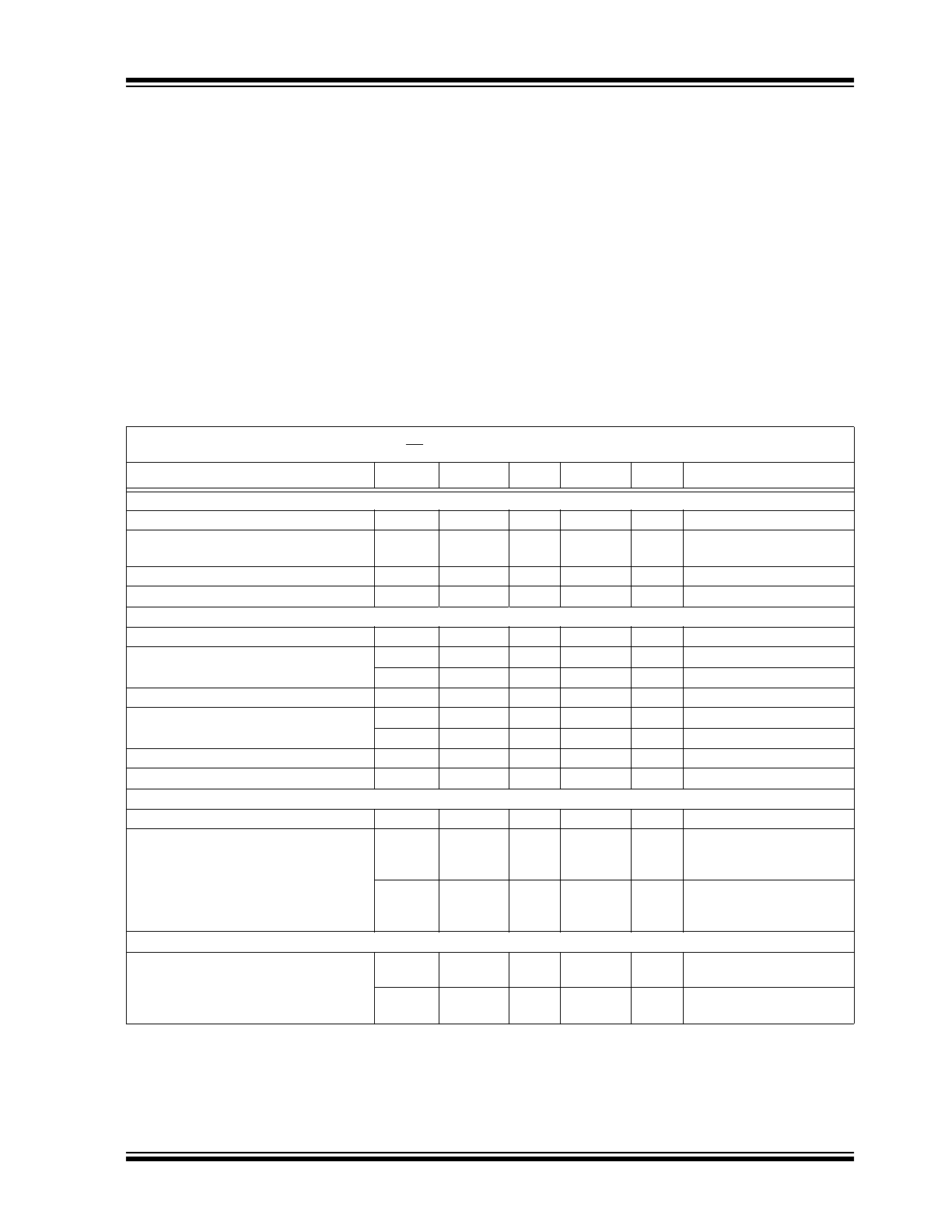
ELECTRICAL CHARACTERISTICS
1.1
Absolute Maximum Ratings †
V
DD
– V
SS
.......................................................................6.5V
Current at Input Pins ....................................................±2 mA
Analog Inputs (V
IN
+ and V
IN
–) †† ... V
SS
– 1.0V to V
DD
+1.0V
All other Inputs and Outputs ............ V
SS
– 0.3V to V
DD
+0.3V
Difference Input voltage ...................................... |V
DD
– V
SS
|
Output Short Circuit Current ................................ Continuous
Current at Output and Supply Pins ............................±30 mA
Storage Temperature ...................................-65°C to +150°C
Max. Junction Temperature ........................................ +150°C
ESD protection on all pins (HBM, MM)
................≥ 4 kV, 300V
†
Notice: Stresses above those listed under “Absolute
Maximum Ratings” may cause permanent damage to the
device. This is a stress rating only and functional operation of
the device at those or any other conditions above those
indicated in the operational listings of this specification is not
implied. Exposure to maximum rating conditions for extended
periods may affect device reliability.
††
See Section 4.2.1 “Rail-to-Rail Inputs”.
1.2
Specifications
TABLE 1-1:
DC ELECTRICAL SPECIFICATIONS
Electrical Characteristics: Unless otherwise indicated, T
A
= +25°C, V
DD
= +1.8V to +5.5V, V
SS
= GND, V
CM
= V
DD
/3,
V
OUT
= V
DD
/2, V
L
= V
DD
/2, R
L
= 20 k
Ω to V
L
, and CS = GND (refer to
Figure 1-5
and
Figure 1-6
).
Parameters
Sym
Min
Typ
Max
Units
Conditions
Input Offset
Input Offset Voltage
V
OS
-2.0
—
+2.0
µV
T
A
= +25°C (Note 1)
Input Offset Voltage Drift with Temperature
(linear Temp. Co.)
TC
1
-50
—
+50
nV/°C
T
A
= -40 to +125°C
(Note 1)
Input Offset Voltage Quadratic Temp. Co.
TC
2
—
±0.1
—
nV/°C
2
T
A
= -40 to +125°C
Power Supply Rejection
PSRR
130
143
—
dB
(Note 1)
Input Bias Current and Impedance
Input Bias Current
I
B
—
±1
—
pA
Input Bias Current across Temperature
I
B
—
60
—
pA
T
A
= +85°C
I
B
—
600
5000
pA
T
A
= +125°C
Input Offset Current
I
OS
—
-30
—
pA
Input Offset Current across Temperature
I
OS
—
-50
—
pA
T
A
= +85°C
I
OS
-1000
-75
1000
pA
T
A
= +125°C
Common Mode Input Impedance
Z
CM
—
10
13
||6
—
Ω||pF
Differential Input Impedance
Z
DIFF
—
10
13
||6
—
Ω||pF
Common Mode
Common-Mode Input Voltage Range
V
CMR
V
SS
− 0.20
—
V
DD
+ 0.20
V
(Note 2)
Common-Mode Rejection
CMRR
130
142
—
dB
V
DD
= 1.8V,
V
CM
= -0.2V to 2.0V
(Note 1, Note 2)
CMRR
140
152
—
dB
V
DD
= 5.5V,
V
CM
= -0.2V to 5.7V
(Note 1, Note 2)
Open-Loop Gain
DC Open-Loop Gain (large signal)
A
OL
130
145
—
dB
V
DD
= 1.8V,
V
OUT
= 0.2V to 1.6V (Note 1)
A
OL
140
156
—
dB
V
DD
= 5.5V,
V
OUT
= 0.2V to 5.3V (Note 1)
Note 1:
Set by design and characterization. Due to thermal junction and other effects in the production environment, these parts
can only be screened in production (except TC
1
; see Appendix B: “Offset Related Test Screens”).
2:
Figure 2-18
shows how V
CMR
changed across temperature for the first three production lots.
MCP6V01/2/3
DS22058C-page 4
© 2008 Microchip Technology Inc.
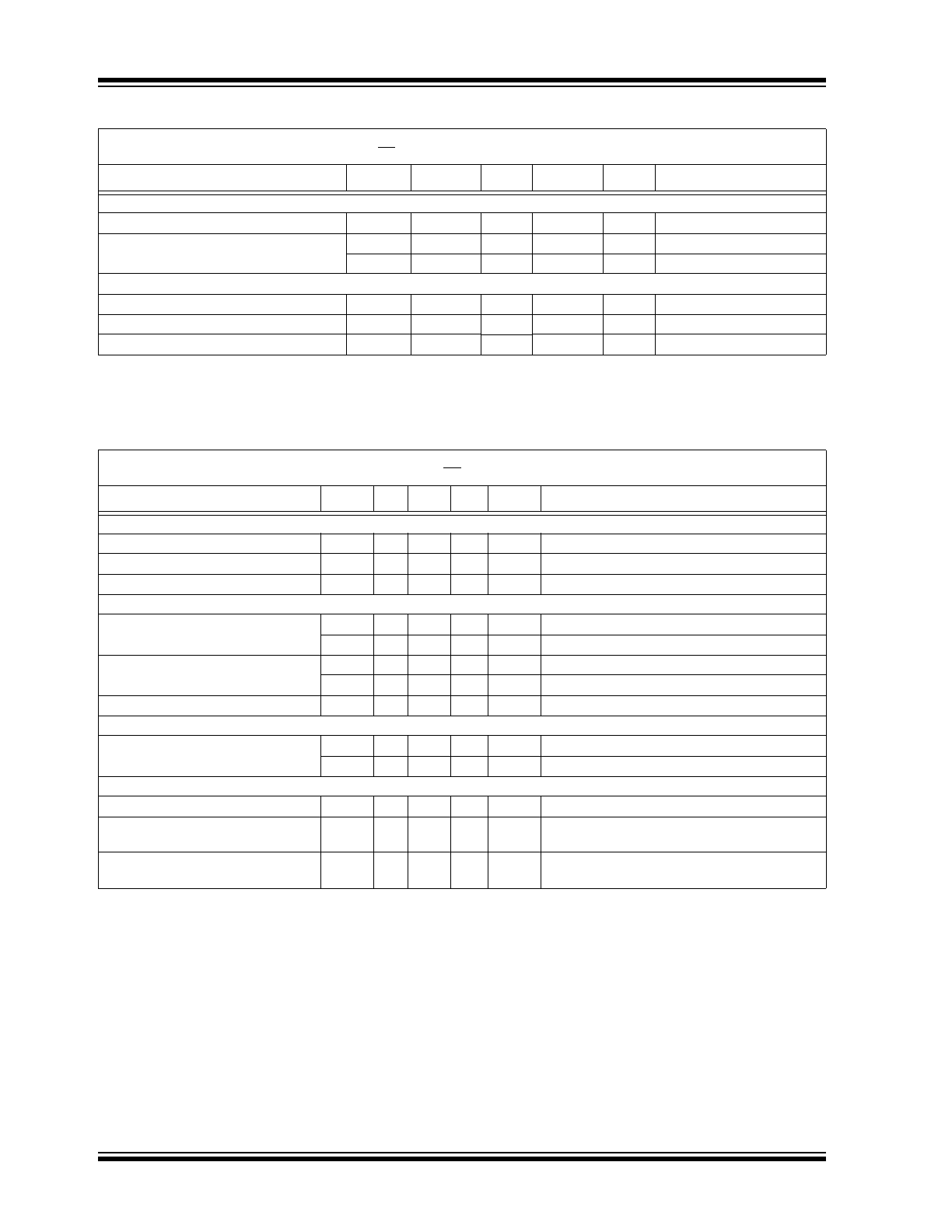
Output
Maximum Output Voltage Swing
V
OL
, V
OH
V
SS
+ 15
—
V
DD
− 15
mV
G = +2, 0.5V input overdrive
Output Short Circuit Current
I
SC
—
±7
—
mA
V
DD
= 1.8V
I
SC
—
±22
—
mA
V
DD
= 5.5V
Power Supply
Supply Voltage
V
DD
1.8
—
5.5
V
Quiescent Current per amplifier
I
Q
200
300
400
µA
I
O
= 0
POR Trip Voltage
V
POR
1.15
—
1.65
V
TABLE 1-1:
DC ELECTRICAL SPECIFICATIONS (CONTINUED)
Electrical Characteristics: Unless otherwise indicated, T
A
= +25°C, V
DD
= +1.8V to +5.5V, V
SS
= GND, V
CM
= V
DD
/3,
V
OUT
= V
DD
/2, V
L
= V
DD
/2, R
L
= 20 k
Ω to V
L
, and CS = GND (refer to
Figure 1-5
and
Figure 1-6
).
Parameters
Sym
Min
Typ
Max
Units
Conditions
Note 1:
Set by design and characterization. Due to thermal junction and other effects in the production environment, these parts
can only be screened in production (except TC
1
; see Appendix B: “Offset Related Test Screens”).
2:
Figure 2-18
shows how V
CMR
changed across temperature for the first three production lots.
TABLE 1-2:
AC ELECTRICAL SPECIFICATIONS
Electrical Characteristics: Unless otherwise indicated, T
A
= +25°C, V
DD
= +1.8V to +5.5V, V
SS
= GND, V
CM
= V
DD
/3,
V
OUT
= V
DD
/2, V
L
= V
DD
/2, R
L
= 20 k
Ω to V
L
, C
L
= 60 pF, and CS = GND (refer to
Figure 1-5
and
Figure 1-6
).
Parameters
Sym
Min Typ Max Units
Conditions
Amplifier AC Response
Gain Bandwidth Product
GBWP
—
1.3
—
MHz
Slew Rate
SR
—
0.5
—
V/µs
Phase Margin
PM
—
65
—
°
G = +1
Amplifier Noise Response
Input Noise Voltage
E
ni
—
0.79
—
µV
P-P
f = 0.01 Hz to 1 Hz
E
ni
—
2.5
—
µV
P-P
f = 0.1 Hz to 10 Hz
Input Noise Voltage Density
e
ni
—
120
—
nV/
√Hz f < 2.5 kHz
e
ni
—
45
—
nV/
√Hz f = 100 kHz
Input Noise Current Density
i
ni
—
0.6
—
fA/
√Hz
Amplifier Distortion (Note 1)
Intermodulation Distortion (AC)
IMD
—
<1
—
µV
PK
V
CM
tone = 50 mV
PK
at 1 kHz, G
N
= 1, V
DD
= 1.8V
IMD
—
<1
—
µV
PK
V
CM
tone = 50 mV
PK
at 1 kHz, G
N
= 1, V
DD
= 5.5V
Amplifier Step Response
Start Up Time
t
STR
—
500
—
µs
V
OS
within 50 µV of its final value
Offset Correction Settling Time
t
STL
—
300
—
µs
G = +1, V
IN
step of 2V,
V
OS
within 50 µV of its final value
Output Overdrive Recovery Time
t
ODR
—
100
—
µs
G = -100, ±0.5V input overdrive to V
DD
/2,
V
IN
50% point to V
OUT
90% point (Note 2)
Note 1:
These parameters were characterized using the circuit in
Figure 1-7
.
Figure 2-37
and
Figure 2-38
show both an IMD
tone at DC and a residual tone at1 kHz; all other IMD and clock tones are spread by the randomization circuitry.
2:
t
ODR
includes some uncertainty due to clock edge timing.
© 2008 Microchip Technology Inc.
DS22058C-page 5
MCP6V01/2/3
TABLE 1-3:
DIGITAL ELECTRICAL SPECIFICATIONS
TABLE 1-4:
TEMPERATURE SPECIFICATIONS
Electrical Characteristics: Unless otherwise indicated, T
A
= +25°C, V
DD
= +1.8V to +5.5V, V
SS
= GND, V
CM
= V
DD
/3,
V
OUT
= V
DD
/2, V
L
= V
DD
/2, R
L
= 20 k
Ω to V
L
, C
L
= 60 pF, and CS = GND (refer to
Figure 1-5
and
Figure 1-6
).
Parameters
Sym
Min
Typ
Max Units
Conditions
CS Pull-Down Resistor (MCP6V03)
CS Pull-Down Resistor
R
PD
3
5
—
M
Ω
CS Low Specifications (MCP6V03)
CS Logic Threshold, Low
V
IL
V
SS
—
0.3V
DD
V
CS Input Current, Low
I
CSL
—
5
—
pA
CS = V
SS
CS High Specifications (MCP6V03)
CS Logic Threshold, High
V
IH
0.7V
DD
—
V
DD
V
CS Input Current, High
I
CSH
—
V
DD
/R
PD
—
pA
CS = V
DD
CS Input High, GND Current per
amplifier
I
SS
—
-0.7
—
µA
CS = V
DD
, V
DD
= 1.8V
I
SS
—
-2.3
—
µA
CS = V
DD
, V
DD
= 5.5V
Amplifier Output Leakage, CS High I
O_LEAK
—
20
—
pA
CS = V
DD
CS Dynamic Specifications (MCP6V03)
CS Low to Amplifier Output On
Turn-on Time
t
ON
—
11
100
µs
CS Low = V
SS
+0.3 V, G = +1 V/V,
V
OUT
= 0.9 V
DD
/2
CS High to Amplifier Output High-Z
t
OFF
—
10
—
µs
CS High = V
DD
– 0.3 V, G = +1 V/V,
V
OUT
= 0.1 V
DD
/2
Internal Hysteresis
V
HYST
—
0.25
—
V
Electrical Characteristics: Unless otherwise indicated, all limits are specified for: V
DD
= +1.8V to +5.5V, V
SS
= GND.
Parameters
Sym
Min
Typ
Max
Units
Conditions
Temperature Ranges
Specified Temperature Range
T
A
-40
—
+125
°C
Operating Temperature Range
T
A
-40
—
+125
°C
(Note 1)
Storage Temperature Range
T
A
-65
—
+150
°C
Thermal Package Resistances
Thermal Resistance, 8L-2x3 TDFN
θ
JA
—
41
—
°C/W
Thermal Resistance, 8L-4x4 DFN
θ
JA
—
44
—
°C/W
(Note 2)
Thermal Resistance, 8L-SOIC
θ
JA
—
150
—
°C/W
Note 1:
Operation must not cause T
J
to exceed Maximum Junction Temperature specification (150°C).
2:
Measured on a standard JC51-7, four layer printed circuit board with ground plane and vias.
MCP6V01/2/3
DS22058C-page 6
© 2008 Microchip Technology Inc.
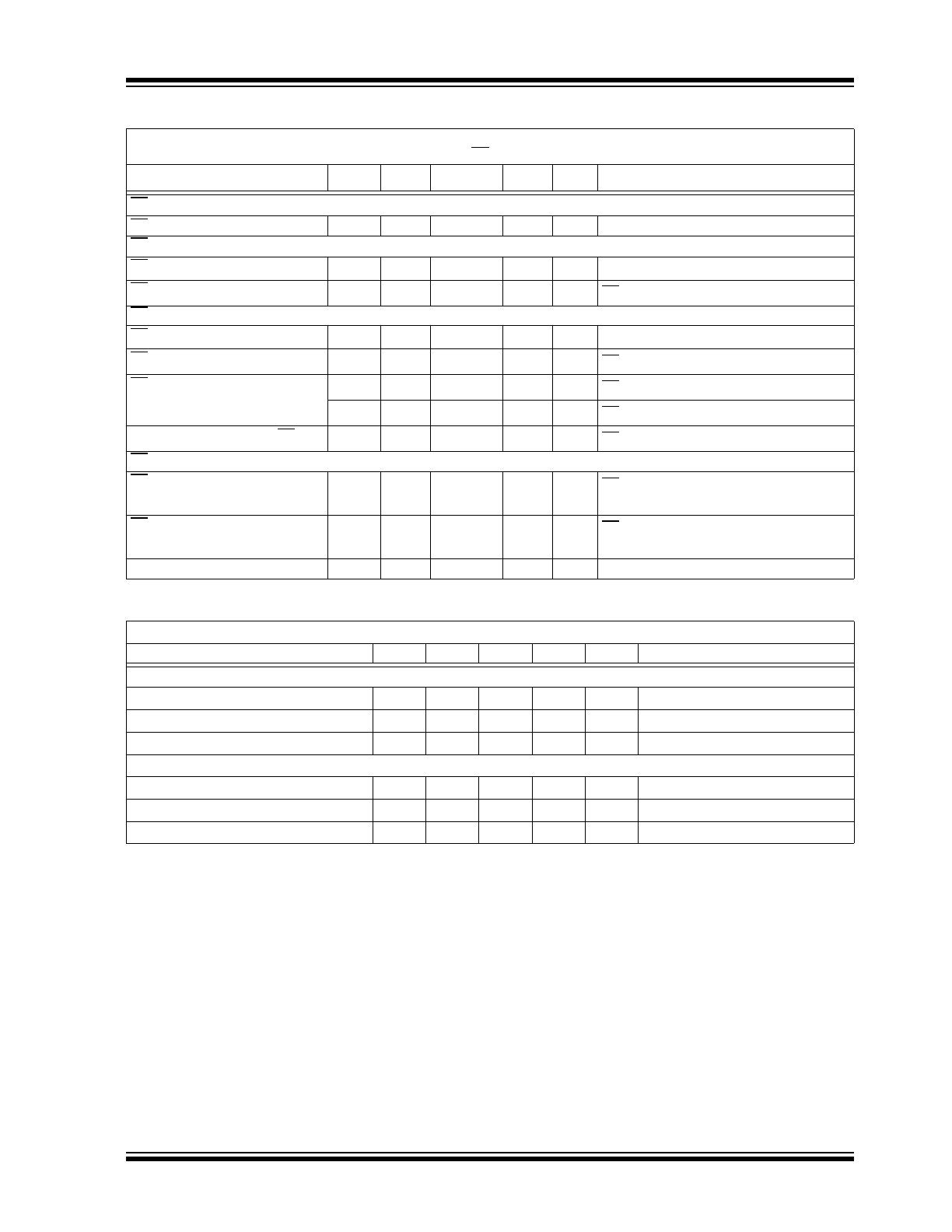
1.3
Timing Diagrams
FIGURE 1-1:
Amplifier Start Up.
FIGURE 1-2:
Offset Correction Settling
Time.
FIGURE 1-3:
Output Overdrive Recovery.
FIGURE 1-4:
Chip Select (MCP6V03).
1.4
Test Circuits
The circuits used for the DC and AC tests are shown in
Figure 1-5
and
Figure 1-6
. Lay the bypass capacitors
out as discussed in Section 4.3.8 “Supply Bypassing
and Filtering”. R
N
is equal to the parallel combination
of R
F
and R
G
to minimize bias current effects.
FIGURE 1-5:
AC and DC Test Circuit for
Most Non-Inverting Gain Conditions.
FIGURE 1-6:
AC and DC Test Circuit for
Most Inverting Gain Conditions.
The circuit in
Figure 1-7
tests the op amp input’s
dynamic behavior (i.e., IMD, t
STR
, t
STL
and t
ODR
). The
potentiometer balances the resistor network (V
OUT
should equal V
REF
at DC). The op amp’s common
mode input voltage is V
CM
= V
IN
/2. The error at the
input (V
ERR
) appears at V
OUT
with a noise gain of
10 V/V.
FIGURE 1-7:
Test Circuit for Dynamic
Input Behavior.
V
DD
V
OS
V
OS
+ 50 µV
V
OS
– 50 µV
t
STR
0V
1.8V to 5.5V
1.8V
V
IN
V
OS
V
OS
+ 50 µV
V
OS
+ 50 µV
t
STL
V
IN
V
OUT
V
DD
V
SS
t
ODR
t
ODR
V
DD
/2
V
IL
High-Z
t
ON
V
IH
CS
t
OFF
V
OUT
-2 µA
High-Z
I
SS
-2 µA
300 µA
1 µA
I
DD
1 µA
300 µA
V
DD
/5 M
Ω
I
CS
V
DD
/5 M
Ω
5 pA
(typical)
(typical)
(typical)
(typical)
(typical)
(typical)
(typical)
(typical)
(typical)
V
DD
MCP6V0X
R
G
R
F
R
N
V
OUT
V
IN
V
DD
/3
1 µF
C
L
R
L
V
L
100 nF
R
ISO
V
DD
MCP6V0X
R
G
R
F
R
N
V
OUT
V
DD
/3
V
IN
1 µF
C
L
R
L
V
L
100 nF
R
ISO
V
DD
MCP6V0X
V
OUT
1 µF
C
L
R
L
V
L
100 nF
R
ISO
20.0 k
Ω
24.9
Ω
20.0 k
Ω
50
Ω
V
IN
V
REF
0.1%
0.1%
25 turn
20.0 k
Ω
20.0 k
Ω
0.1%
0.1%
2.4
9
kΩ
2.
49
kΩ
© 2008 Microchip Technology Inc.
DS22058C-page 7
MCP6V01/2/3
2.0
TYPICAL PERFORMANCE CURVES
Note: Unless otherwise indicated, T
A
= +25°C, V
DD
= +1.8V to 5.5V, V
SS
= GND, V
CM
= V
DD
/3, V
OUT
= V
DD
/2,
V
L
= V
DD
/2, R
L
= 20 k
Ω to V
L
, C
L
= 60 pF, and CS = GND.
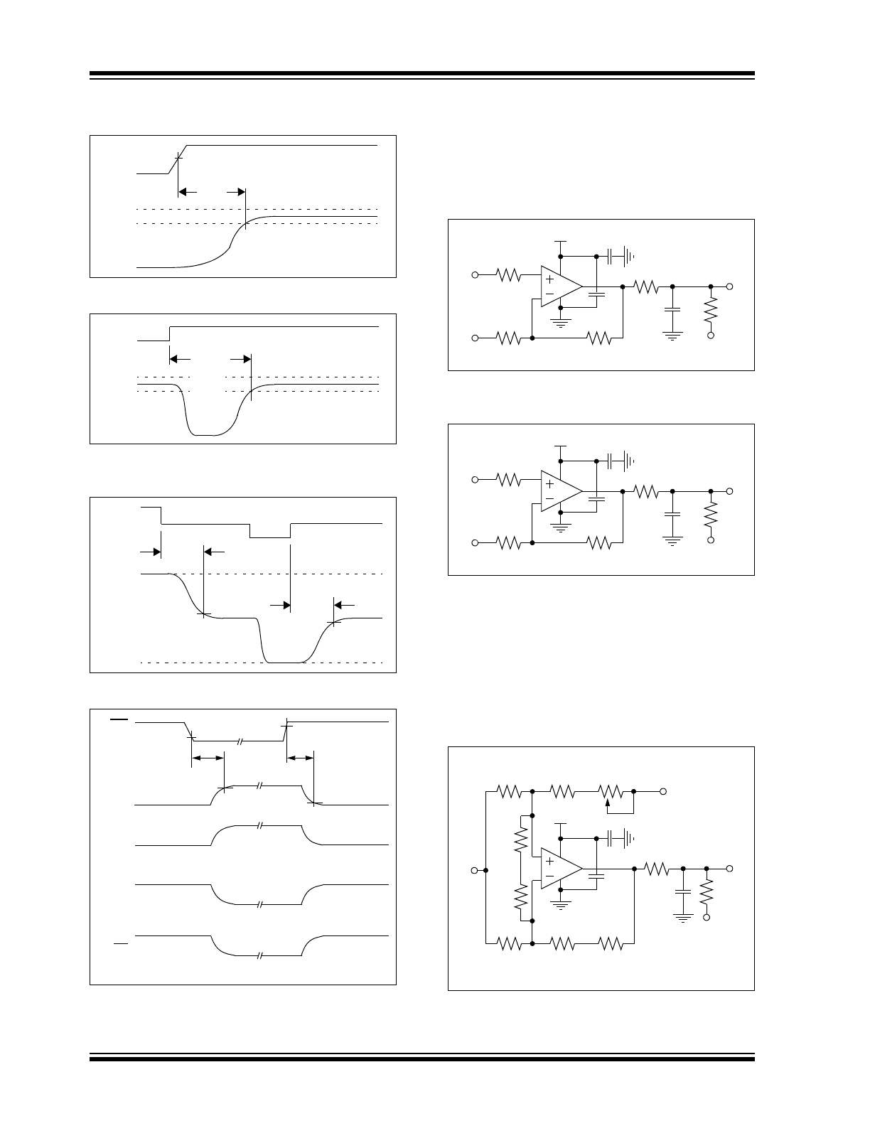
2.1
DC Input Precision
FIGURE 2-1:
Input Offset Voltage.
FIGURE 2-2:
Input Offset Voltage Drift.
FIGURE 2-3:
Input Offset Voltage
Quadratic Temp Co.
FIGURE 2-4:
Input Offset Voltage vs.
Power Supply Voltage with V
CM
= V
CMR_L
.
FIGURE 2-5:
Input Offset Voltage vs.
Power Supply Voltage with V
CM
= V
CMR_H
.
FIGURE 2-6:
Input Offset Voltage vs.
Output Voltage.
Note:
The graphs and tables provided following this note are a statistical summary based on a limited number of
samples and are provided for informational purposes only. The performance characteristics listed herein
are not tested or guaranteed. In some graphs or tables, the data presented may be outside the specified
operating range (e.g., outside specified power supply range) and therefore outside the warranted range.
0%
2%
4%
6%
8%
10%
12%
14%
16%
18%
20%
-1
.5
-1
.0
-0
.5
0.
0
0.
5
1.
0
1.
5
Input Offset Voltage (µV)
Perc
en
ta
g
e o
f O
ccu
rre
nc
es
78 Samples
T
A
= +25°C
V
DD
= 1.8V and 5.5V
Soldered on PCB
0%
2%
4%
6%
8%
10%
12%
14%
16%
18%
20%
22%
-5
0
-4
0
-3
0
-2
0
-1
0
0
10
20
30
40
50
Input Offset Voltage Drift; TC
1
(nV/°C)
P
e
rc
e
n
ta
ge
of
O
c
c
u
rr
e
nc
e
s
78 Samples
V
DD
= 1.8V and 5.5V
Soldered on PCB
0%
2%
4%
6%
8%
10%
12%
14%
16%
18%
20%
22%
-0
.4
-0
.3
-0
.2
-0
.1
0.0
0.
1
0.
2
0.
3
0.4
Input Offset Voltage's Quadratic Temp Co;
TC
2
(nV/°C
2
)
P
e
rc
e
n
ta
g
e
o
f
O
c
cu
rr
en
ce
s
78 Samples
V
DD
= 1.8V and 5.5V
Soldered on PCB
-4
-3
-2
-1
0
1
2
3
4
0.0 0.5 1.0 1.5 2.0 2.5 3.0 3.5 4.0 4.5 5.0 5.5 6.0 6.5
Power Supply Voltage (V)
Input
O
ff
s
e
t V
o
lt
a
g
e
(
µ
V
)
+125°C
+85°C
+25°C
-40°C
V
CM
= V
CMR_L
Representative Part
-4
-3
-2
-1
0
1
2
3
4
0.0 0.5 1.0 1.5 2.0 2.5 3.0 3.5 4.0 4.5 5.0 5.5 6.0 6.5
Power Supply Voltage (V)
Input
O
ffs
e
t V
o
lt
a
g
e
(µ
V
)
+125°C
+85°C
+25°C
-40°C
V
CM
= V
CMR_H
Representative Part
-4
-3
-2
-1
0
1
2
3
4
0.0 0.5 1.0 1.5 2.0 2.5 3.0 3.5 4.0 4.5 5.0 5.5
Output Voltage (V)
Input
O
ffs
e
t V
o
lt
a
g
e
(µ
V
)
V
DD
= 1.8V
V
DD
= 5.5V
Representative Part
MCP6V01/2/3
DS22058C-page 8
© 2008 Microchip Technology Inc.
Note: Unless otherwise indicated, T
A
= +25°C, V
DD
= +1.8V to 5.5V, V
SS
= GND, V
CM
= V
DD
/3, V
OUT
= V
DD
/2,
V
L
= V
DD
/2, R
L
= 20 k
Ω to V
L
, C
L
= 60 pF, and CS = GND.
FIGURE 2-7:
Input Offset Voltage vs.
Common Mode Voltage with V
DD
= 1.8V.
FIGURE 2-8:
Input Offset Voltage vs.
Common Mode Voltage with V
DD
= 5.5V.
FIGURE 2-9:
CMRR.
FIGURE 2-10:
PSRR.
FIGURE 2-11:
DC Open-Loop Gain.
FIGURE 2-12:
CMRR and PSRR vs.
Ambient Temperature.
-4
-3
-2
-1
0
1
2
3
4
-0
.6
-0
.4
-0
.2
0.
0
0.
2
0.
4
0.
6
0.
8
1.
0
1.
2
1.
4
1.
6
1.
8
2.
0
2.
2
2.
4
Input Common Mode Voltage (V)
Input
O
ffs
e
t V
o
lt
a
g
e
(µ
V
)
V
DD
= 1.8V
Representative Part
+125°C
+85°C
+25°C
-40°C
-4
-3
-2
-1
0
1
2
3
4
-0.
5
0.
0
0.
5
1.
0
1.
5
2.
0
2.
5
3.
0
3.
5
4.
0
4.
5
5.
0
5.
5
6.
0
Input Common Mode Voltage (V)
Input
O
ffs
e
t V
o
lt
a
g
e
(µ
V
)
V
DD
= 5.5V
Representative Part
+125°C
+85°C
+25°C
-40°C
0%
5%
10%
15%
20%
25%
30%
35%
-0
.3
-0
.2
-0
.1
0.0
0.1
0.2
0.3
1/CMRR (µV/V)
Pe
rcen
ta
g
e of
Occ
u
rr
en
ce
s
39 Samples
T
A
= +25°C
Soldered on PCB
V
DD
= 1.8V
V
DD
= 5.5V
0%
2%
4%
6%
8%
10%
12%
14%
-0
.3
-0
.2
-0
.1
0.
0
0.
1
0.
2
0.
3
1/PSRR (µV/V)
Pe
rcen
ta
g
e of
Occ
u
rr
en
ce
s
40 Samples
T
A
= +25°C
Soldered on PCB
0%
5%
10%
15%
20%
25%
30%
35%
40%
45%
50%
55%
-0
.3
-0
.2
-0
.1
0.
0
0.
1
0.
2
0.
3
1/A
OL
(µV/V)
Per
cen
ta
g
e of
Occ
u
rr
en
ces
40 Samples
T
A
= +25°C
V
DD
= 1.8V
V
DD
= 5.5V
120
125
130
135
140
145
150
155
160
-50
-25
0
25
50
75
100
125
Ambient Temperature (°C)
CM
RR
, P
S
RR
(
d
B
)
PSRR
CMRR
V
DD
= 5.5V
V
DD
= 1.8V
© 2008 Microchip Technology Inc.
DS22058C-page 9
MCP6V01/2/3
Note: Unless otherwise indicated, T
A
= +25°C, V
DD
= +1.8V to 5.5V, V
SS
= GND, V
CM
= V
DD
/3, V
OUT
= V
DD
/2,
V
L
= V
DD
/2, R
L
= 20 k
Ω to V
L
, C
L
= 60 pF, and CS = GND.
FIGURE 2-13:
DC Open-Loop Gain vs.
Ambient Temperature.
FIGURE 2-14:
Input Bias and Offset
Currents vs. Common Mode Input Voltage with
T
A
= +85°C.
FIGURE 2-15:
Input Bias and Offset
Currents vs. Common Mode Input Voltage with
T
A
= +125°C.
FIGURE 2-16:
Input Bias and Offset
Currents vs. Ambient Temperature with
V
DD
= +5.5V.
FIGURE 2-17:
Input Bias Current vs. Input
Voltage (below V
SS
).
120
125
130
135
140
145
150
155
160
-50
-25
0
25
50
75
100
125
Ambient Temperature (°C)
D
C
O
p
e
n
-L
oop
G
a
in
(d
B)
V
DD
= 5.5V
V
DD
= 1.8V
-60
-40
-20
0
20
40
60
80
100
120
140
160
-0
.5
0.
0
0.5
1.0
1.5
2.0
2.5
3.0
3.
5
4.
0
4.
5
5.0
5.5
6.0
Common Mode Input Voltage (V)
Input
B
ia
s
, O
ff
s
e
t
Cu
rr
e
n
ts
(p
A
)
I
B
T
A
= +85°C
V
DD
= 5.5V
I
OS
-400
-200
0
200
400
600
800
1000
1200
1400
1600
-0
.5
0.
0
0.
5
1.
0
1.
5
2.
0
2.
5
3.
0
3.
5
4.
0
4.
5
5.
0
5.
5
6.
0
Common Mode Input Voltage (V)
Input
B
ia
s
, O
ff
s
e
t Cu
rr
e
n
ts
(p
A
)
I
B
T
A
= +125°C
V
DD
= 5.5V
I
OS
1
10
100
1,000
25 35 45 55 65 75 85 95 105 115 125
Ambient Temperature (°C)
In
pu
t
B
ias
, Of
fset
Cu
rre
nt
s
(p
A)
V
DD
= 5.5V
-I
OS
I
B
1.E-12
1.E-11
1.E-10
1.E-09
1.E-08
1.E-07
1.E-06
1.E-05
1.E-04
1.E-03
1.E-02
-1.0 -0.9 -0.8 -0.7 -0.6 -0.5 -0.4 -0.3 -0.2 -0.1 0.0
Input Voltage (V)
Inpu
t
C
u
rre
nt Ma
gnitude
(A)
+125°C
+85°C
+25°C
-40°C
10m
1m
100µ
10µ
1µ
100n
10n
1n
100p
10p
1p
MCP6V01/2/3
DS22058C-page 10
© 2008 Microchip Technology Inc.
Note: Unless otherwise indicated, T
A
= +25°C, V
DD
= +1.8V to 5.5V, V
SS
= GND, V
CM
= V
DD
/3, V
OUT
= V
DD
/2,
V
L
= V
DD
/2, R
L
= 20 k
Ω to V
L
, C
L
= 60 pF, and CS = GND.
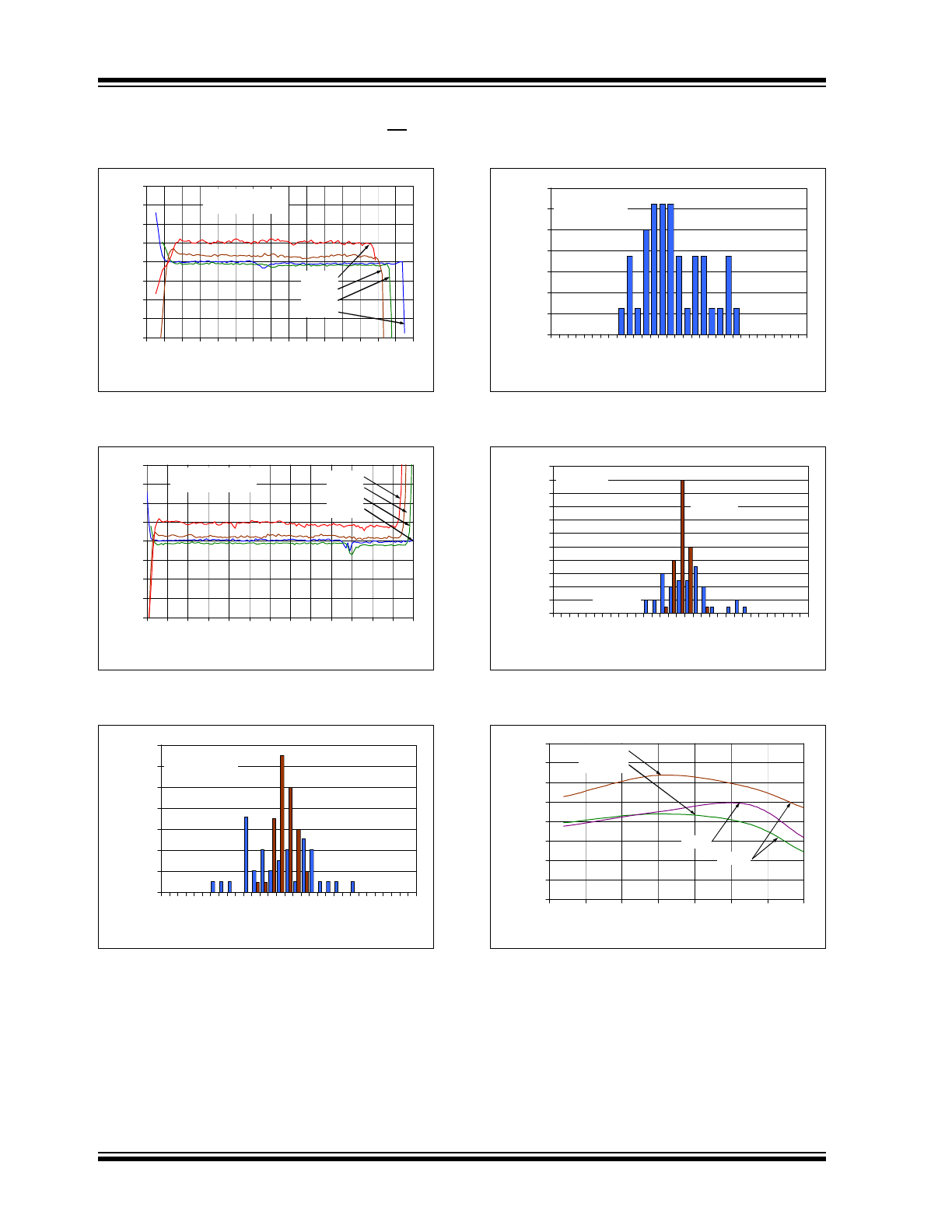
2.2
Other DC Voltages and Currents
FIGURE 2-18:
Input Common Mode
Voltage Headroom (Range) vs. Ambient
Temperature.
FIGURE 2-19:
Output Voltage Headroom
vs. Output Current.
FIGURE 2-20:
Output Voltage Headroom
vs. Ambient Temperature.
FIGURE 2-21:
Output Short Circuit Current
vs. Power Supply Voltage.
FIGURE 2-22:
Supply Current vs. Power
Supply Voltage.
FIGURE 2-23:
Power On Reset Trip
Voltage.
-0.35
-0.30
-0.25
-0.20
-0.15
-0.10
-0.05
0.00
0.05
-50
-25
0
25
50
75
100
125
Ambient Temperature (°C)
Input
C
o
mmon Mod
e
Volta
g
e
H
ead
ro
om
(
V
)
Lower (V
CMR
– V
SS
)
Upper ( V
DD
– V
CMR
)
3 Lots
10
100
1000
0.1
1
10
Output Current Magnitude (mA)
O
u
tput V
o
lt
a
g
e
He
a
d
room
(m
V
)
V
DD
– V
OH
V
DD
= 5.5V
V
OL
– V
SS
V
DD
= 1.8V
0
1
2
3
4
5
6
7
8
9
10
11
12
-50
-25
0
25
50
75
100
125
Ambient Temperature (°C)
Outpu
t H
ead
ro
om (mV
)
V
DD
– V
OH
V
DD
= 5.5V
V
OL
– V
SS
V
DD
= 1.8V
R
L
= 20 kΩ
-40
-30
-20
-10
0
10
20
30
40
0.
0
0.
5
1.
0
1.
5
2.
0
2.
5
3.
0
3.
5
4.
0
4.
5
5.
0
5.
5
6.
0
6.
5
Power Supply Voltage (V)
Outpu
t S
h
ort C
irc
ui
t
Cu
rre
n
t
(mA)
-40°C
+25°C
+85°C
+125°C
+125°C
+85°C
+25°C
-40°C
0
50
100
150
200
250
300
350
400
450
0.
0
0.
5
1.
0
1.
5
2.
0
2.
5
3.
0
3.
5
4.
0
4.
5
5.
0
5.
5
6.
0
6.
5
Power Supply Voltage (V)
Su
pply C
u
rr
en
t
(µ
A)
+125°C
+85°C
+25°C
-40°C
0%
5%
10%
15%
20%
25%
30%
1.1
1.2
1.3
1.
4
1.
5
1.6
1.7
POR Trip Voltage (V)
Pe
rc
en
ta
g
e
o
f
O
c
cu
rr
en
c
e
s
93 Samples
3 Lots
T
A
= +25°C