
© 2007 Microchip Technology Inc.
DS21384D-page 1
TC1278/TC1279
Features
• Precision V
CC
Monitor for 5.0V System Supplies
• 250 ms Minimum RESET Output Duration
• Output Valid to V
CC
= 1.2V
• V
CC
Transient Immunity
• Small 3-Pin SOT-23 Package
• No External Components
• Internal Pull-up Resistor
• Available in 3 different voltage detection levels:
- 4.625V (typ.), -5 suffix
- 4.375V (typ.), -10 suffix
- 4.125V (typ.), -15 suffix
Applications
• Computers
• Embedded Systems
• Battery Powered Equipment
• Critical µP Power Supply Monitoring
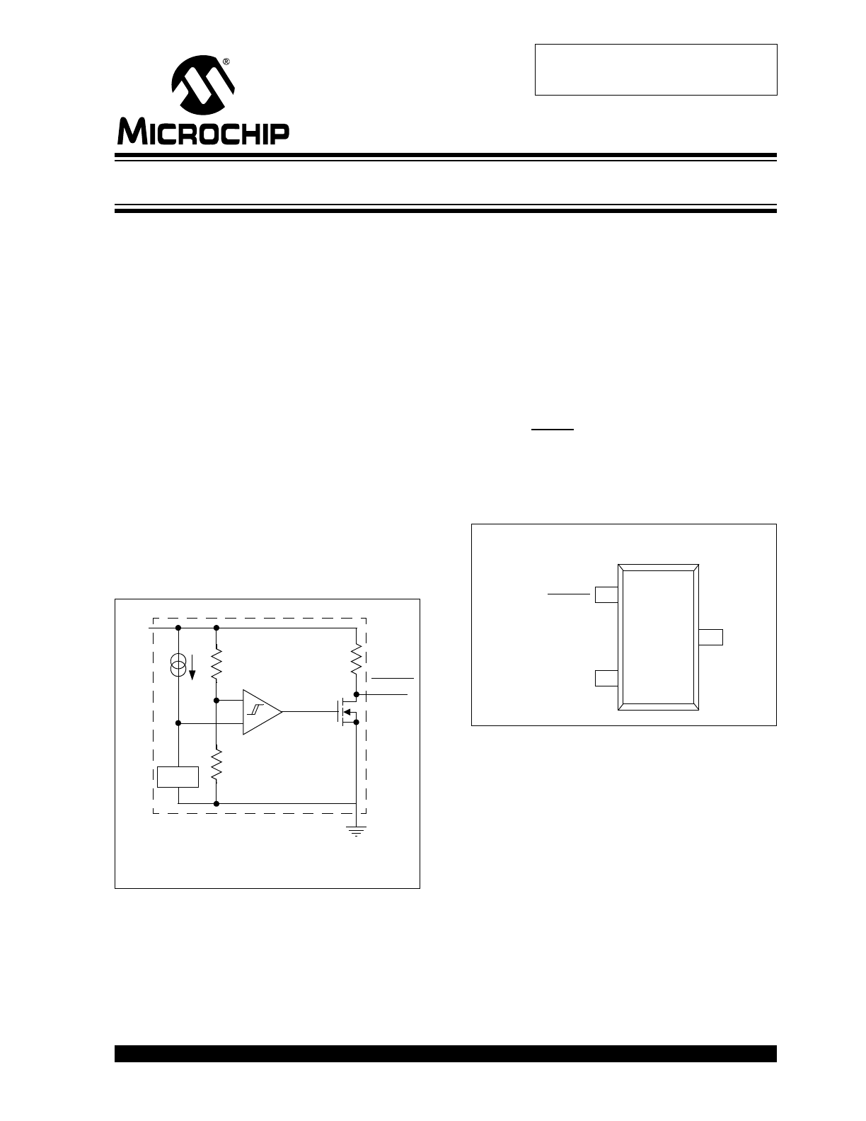
Typical Operating Circuit
General Description
The TC1278/TC1279 are cost-effective system super-
visor circuits designed to monitor V
CC
in digital systems
and provide a reset signal to the host processor when
necessary. No external components are required. The
open-drain output uses an internal pull-up resistor of
approximately 6 k
Ω.
The reset output is driven active within 5 µs of V
CC
falling through the reset voltage threshold. RESET is
maintained active for a minimum of 250 ms after V
CC
rises above the reset threshold. The TC1278 has an
active-high RESET output, while the TC1279 has an
active-low RESET output, with both devices having an
open-drain output stage. The output is valid down to
V
CC
= 1.2V. Both devices are available in a 3-Pin
SOT- 23 package.
Package Type
RESET
GND
+
–
V
CC
V
REF
Internal
Pull-up
6 k
Ω
Resistor
TC1279
TC1278 has an active-high RESET output.
V
CC
(TC1278) RESET
GND
TC1278
TC1279
1
2
3
3-Pin SOT-23
(TC1279) RESET
3-Pin Reset Monitors for 5V Systems
Obsolete Device
TC1278/TC1279
DS21384D-page 2
© 2007 Microchip Technology Inc.
1.0
ELECTRICAL
CHARACTERISTICS
Absolute Maximum Ratings †
Supply Voltage (V
CC
to GND)..............................+6.0V
RESET, RESET...........................-0.3V to (V
CC
+ 0.3V)
Input Current, V
CC
..............................................20 mA
Output Current, RESET......................................20 mA
Power Dissipation (T
A
≤ 70°C)
3-Pin SOT-23 (derate 4mW/°C above +70°C)
................................................................230 mW
Operating Temperature Range.............-40°C to +85°C
Storage Temperature Range ..............-65°C to +150°C
† Stresses above those listed under "Absolute Maximum
Ratings" may cause permanent damage to the device. These
are stress ratings only and functional operation of the device
at these or any other conditions above those indicated in the
operation sections of the specifications is not implied.
Exposure to Absolute Maximum Rating conditions for
extended periods may affect device reliability.
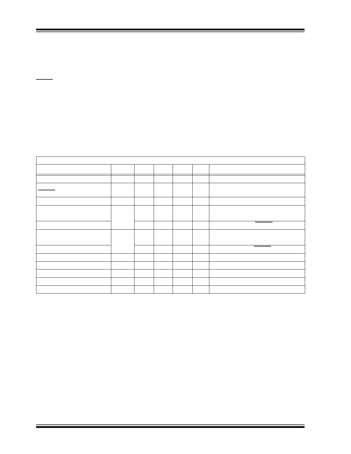
DC CHARACTERISTICS
Electrical Specifications: Unless otherwise indicated, T
A
= -40°C to +85°C. Typical values are at T
A
= +25°C.
Parameters
Sym
Min
Typ
Max
Units
Conditions
Supply Voltage
V
CC
1.2
—
5.5
V
Note 1
Low Level @ RESET (TC1278)
RESET (TC1279)
V
OL
—
—
0.4
V
Note 1
Output Current @ 0.4 Volts
I
OL
+8
—
—
mA
Note 2
Operating Current:
TC1278
I
CC1
—
0.9
2.0
mA
V
CC
> V
CCTP(MAX)
, RESET = 1, (Note 3)
TC1279
—
—
40
µA
V
CC
> V
CCTP(MAX)
, RESET = 1, Note 4
Operating Current:
TC1278
I
CC2
—
—
40
µA
V
CC
< V
CCTP(MIN)
, RESET = 0, (Note 4)
TC1279
—
0.9
2.0
mA
V
CC
< V
CCTP(MIN)
, RESET = 0,
(Note 3)
V
CC
Trip Point (TC1278/9-5)
V
CCTP-5
4.50
4.625
4.74
V
Note 1
V
CC
Trip Point (TC1278/9-10)
V
CCTP-10
4.25
4.375
4.49
V
Note 1
V
CC
Trip Point (TC1278/9-15)
V
CCTP-15
4.00
4.125
4.24
V
Note 1
Output Capacitance
C
OUT
—
9
—
pF
Internal Pull-Up Resistor
R
P
3
6
9
k
Ω
Note 1: All voltages referenced to ground.
2: A 1 k
Ω external resistor may be required in some applications for proper operation of the microprocessor
reset control circuit when using the TC1279. V
CC
= 1.8V.
3: Operating current is specified with the open-drain output in the active (“ON”) condition.
4: Operating current is specified with the open-drain output in the non-active (“OFF”) condition.
© 2007 Microchip Technology Inc.
DS21384D-page 3
TC1278/TC1279
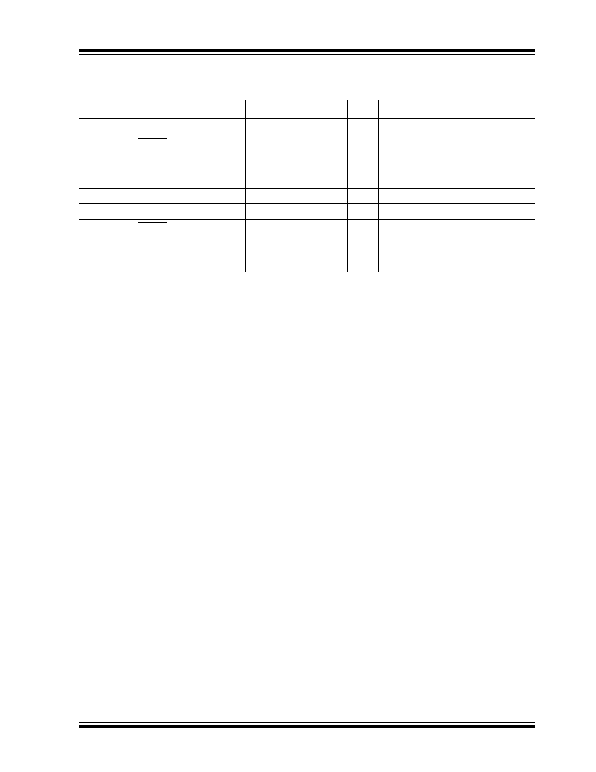
AC CHARACTERISTICS
Electrical Specifications: Unless otherwise indicated, T
A
= -40°C to +85°C. Typical values are at T
A
= +25°C.
Parameters
Sym
Min
Typ
Max
Units
Conditions
RESET Active Time
t
RST
250
350
450
ms
V
CC
Detect to RESET
(TC1279)
t
RPD1
—
2
5
µs
Figure 3-2
V
CC
Detect to RESET
(TC1278)
t
RPD2
—
2
5
µs
Figure 3-4
V
CC
Slew Rate (4.75V-4.00V)
t
F
300
—
—
µs
Figure 3-2
,
Figure 3-4
V
CC
Slew Rate (4.00V-4.75V)
t
R
0
—
—
ns
Figure 3-1
,
Figure 3-3
V
CC
Detect to RESET
(TC1279)
t
RPU1
250
350
450
ms
Figure 3-1
V
CC
Detect to RESET
(TC1278)
t
RPU2
250
350
450
ms
Figure 3-3
TC1278/TC1279
DS21384D-page 4
© 2007 Microchip Technology Inc.
2.0
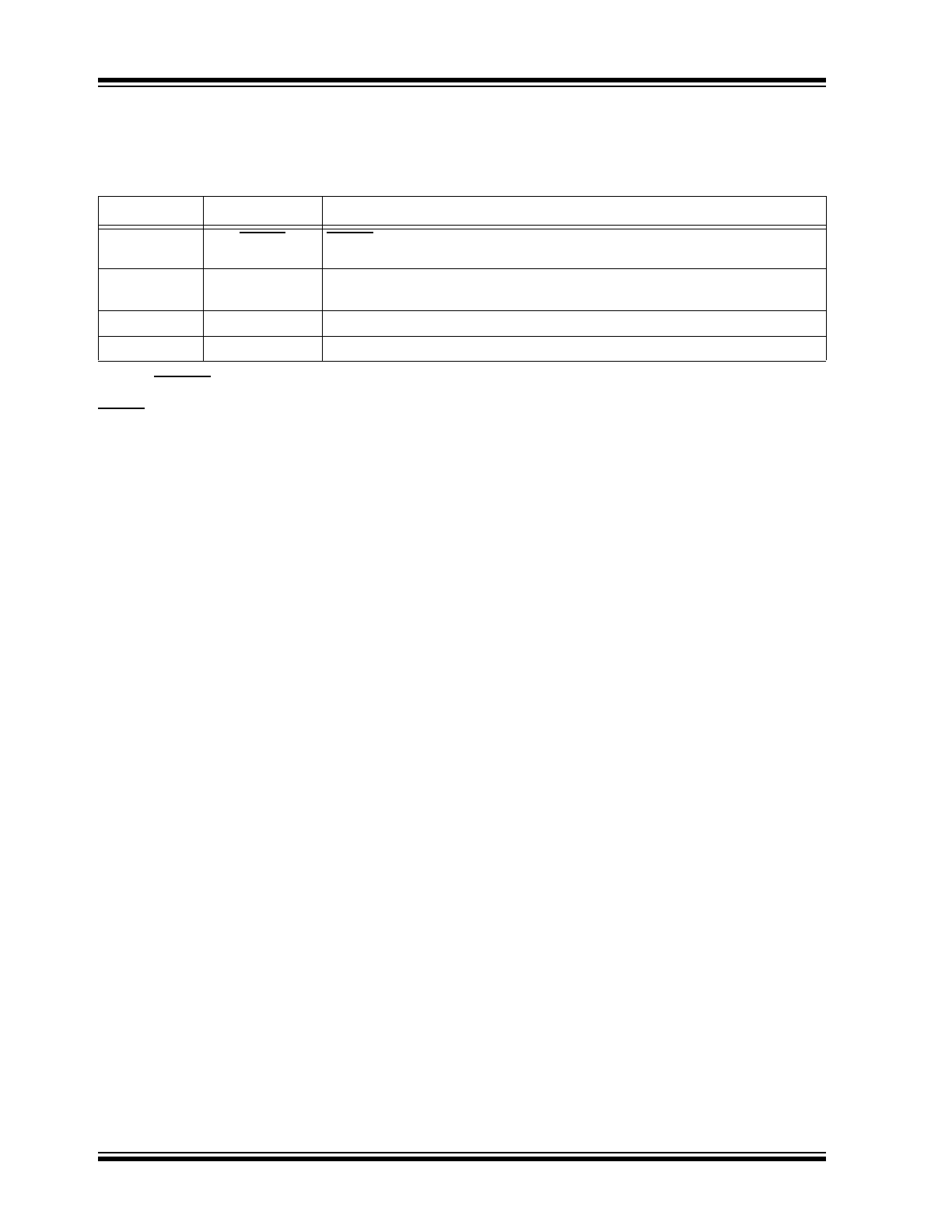
PIN DESCRIPTIONS
The descriptions of the pins are listed in
Table 2-1
.
TABLE 2-1:
PIN FUNCTION TABLE
2.1
RESET (TC1279)
RESET output remains low while V
CC
is below the
reset voltage threshold, and for 350 ms (250 ms min.)
after V
CC
rises above reset threshold. The output stage
of the TC1279 is open-drain.
2.2
RESET (TC1278)
RESET output remains high while V
CC
is below the
reset voltage threshold, and for 350 ms (250 ms min.)
after V
CC
rises above reset threshold. The output stage
of the TC1278 is open-drain.
2.3
V
CC
Supply voltage (1.2V to 5.5V).
2.4
Ground
Device ground.
Pin No.
Symbol
Function
1
RESET
(TC1279)
RESET output
1
RESET
(TC1278)
RESET output
2
V
CC
Supply voltage (1.2V to 5.5V).
3
GND
Ground.
© 2007 Microchip Technology Inc.
DS21384D-page 5
TC1278/TC1279
3.0
APPLICATIONS INFORMATION
3.1
Operation – Power Monitor
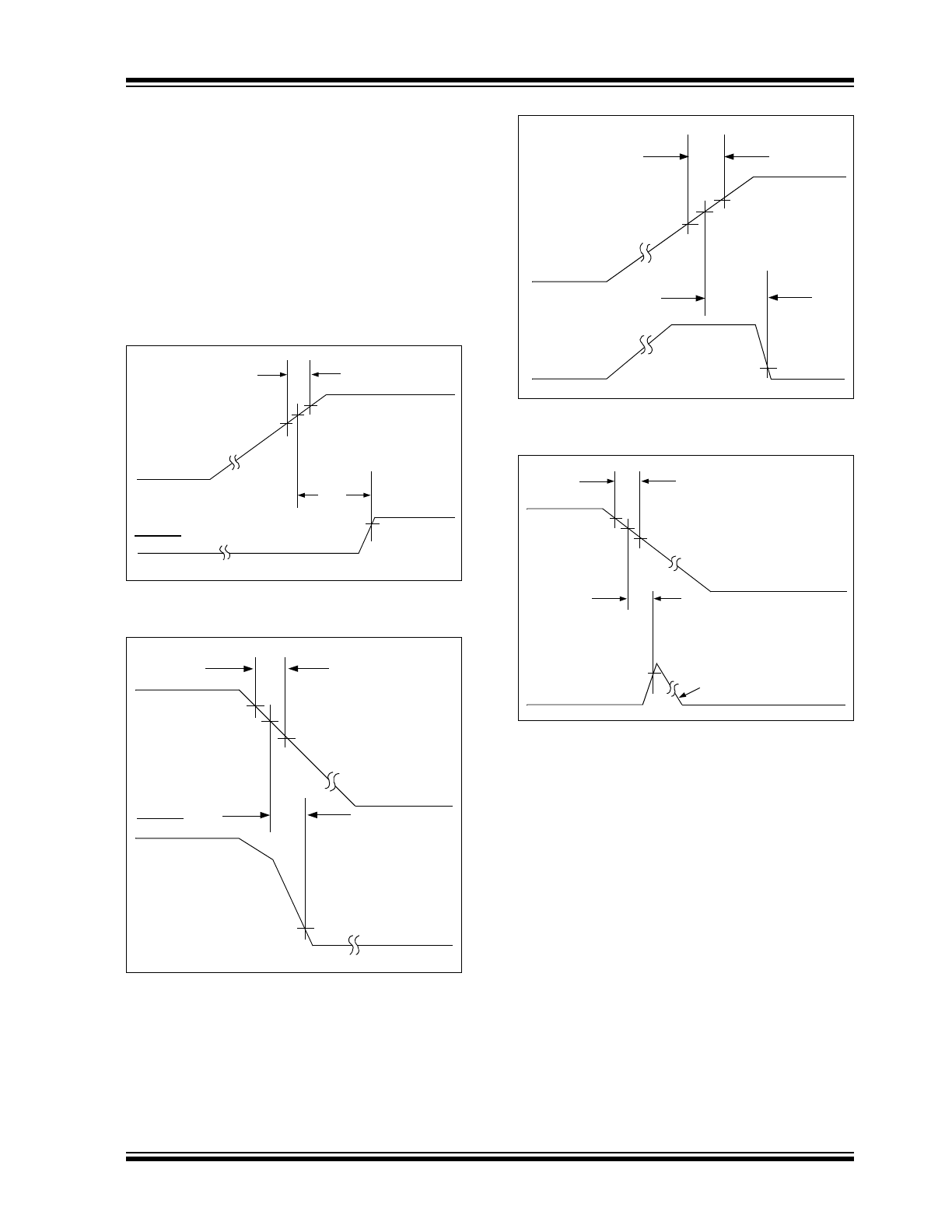
The TC1278/TC1279 provide the function of detecting
out-of-tolerance power supply conditions and warning
a processor-based system of impending power failure.
When V
CC
is detected as out-of-tolerance, the RESET
signal is asserted. On power-up, RESET is kept active
for approximately 350 ms after the power supply has
reached the selected tolerance. This allows the power
supply and microprocessor to stabilize before RESET
is released.
FIGURE 3-1:
TC1279 Power Up Timing
Diagram.
FIGURE 3-2:
TC1279 Power-Down
Timing Diagram.
FIGURE 3-3:
TC1278 Power-Up Timing
Diagram.
FIGURE 3-4:
TC1278 Power-Down
Timing Diagram.
4.75V
4.00V
t
R
V
CCTP
V
CC
RESET
t
RPU1
V
OH
V
CC
RESET
4.75V
V
CCTP
4.00V
V
OL
t
RPD1
t
F
t
R
t
RPU2
V
OL
V
CCTP
V
CC
RESET
V
CCTP(MAX)
V
CCTP(MIN)
t
F
t
RPD2
V
CC
4.74V
V
OH
RESET
V
CCTP
4.00V
RESET SLEWS WITH V
CC
TC1278/TC1279
DS21384D-page 6
© 2007 Microchip Technology Inc.
3.2
V
CC
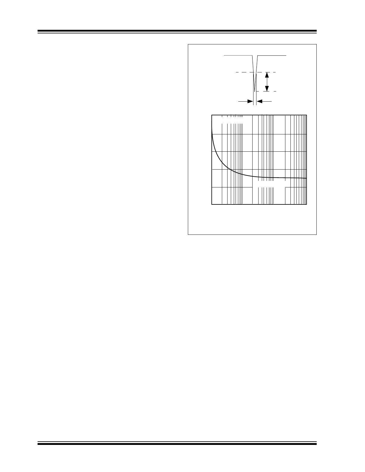
Transient Rejection
The TC1278/TC1279 provides accurate V
CC
monitor-
ing and reset timing during power-up, power-down,
and brownout/sag conditions. Furthermore, it rejects
negative-going transients (glitches) on the power
supply line.
Figure 3-5
shows the maximum transient
duration vs. maximum negative excursion (overdrive)
for glitch rejection. Any combination of duration and
overdrive that lays under the curve will not generate a
reset signal. Combinations above the curve are
detected as a brownout or power-down. Transient
immunity can be improved by adding a capacitor in
close proximity to the V
CC
pin of the TC1278/TC1279.
FIGURE 3-5:
Maximum Transient
Duration vs. Overdrive For Glitch Rejection At
+25°C.
RESET COMPARATOR OVERDRIVE,
[ V
CCTP
- V
CC
] (mV)
5
3
2
4
1
0
1
5
100
1000
MAXIMUM TRANSIENT DURA
TION (µse
c)
T
A
= +25°C
V
CCTP
Duration
Overdrive
V
CC
TC1278/9
© 2007 Microchip Technology Inc.
DS21384D-page 7
TC1278/TC1279
4.0
PACKAGING INFORMATION
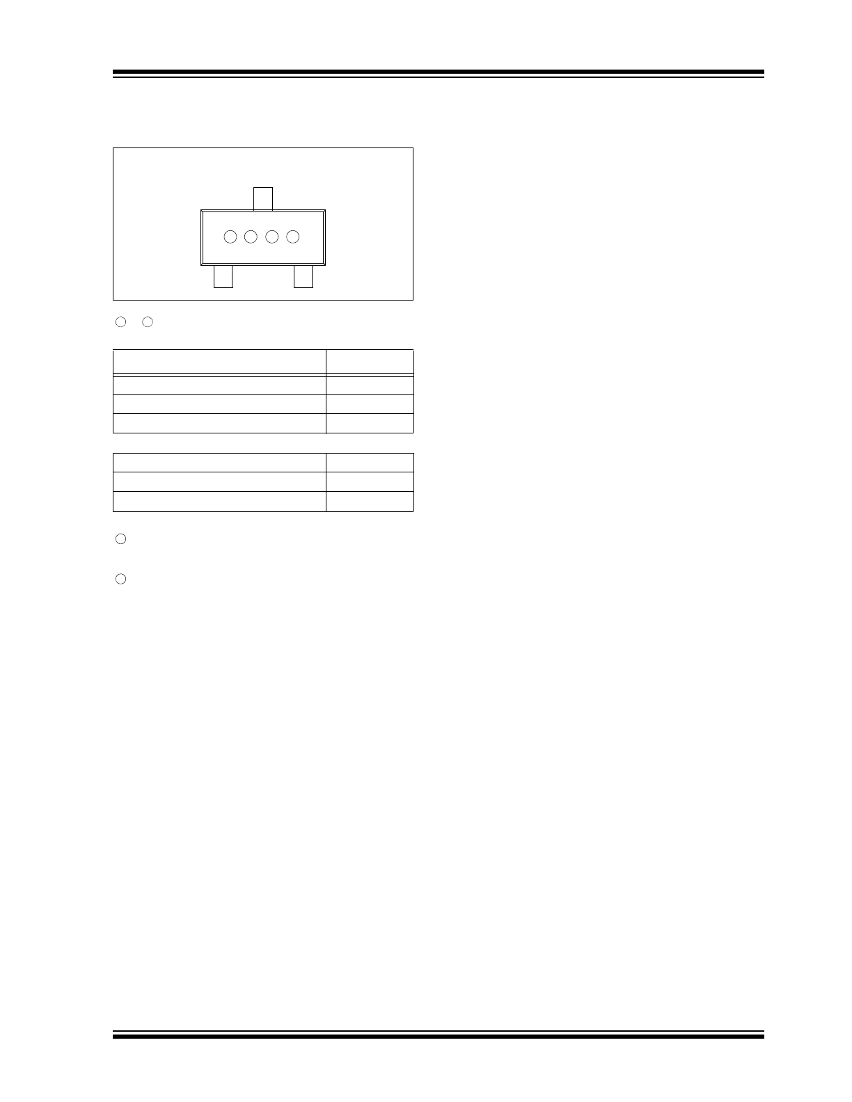
4.1
Package Marking Information
Part Number
Code
TC1278-5ENB
PA
TC1278-10ENB
PB
TC1278-15ENB
PC
TC1279-5ENB
RA
TC1279-10ENB
RB
TC1279-15ENB
RC
3-Pin SOT-23
1 2
4
3
1
&
= part number code + temperature range
2
and voltage
3
represents year and 2-month code
4
represents production lot ID code
TC1278/TC1279
DS21384D-page 8
© 2007 Microchip Technology Inc.
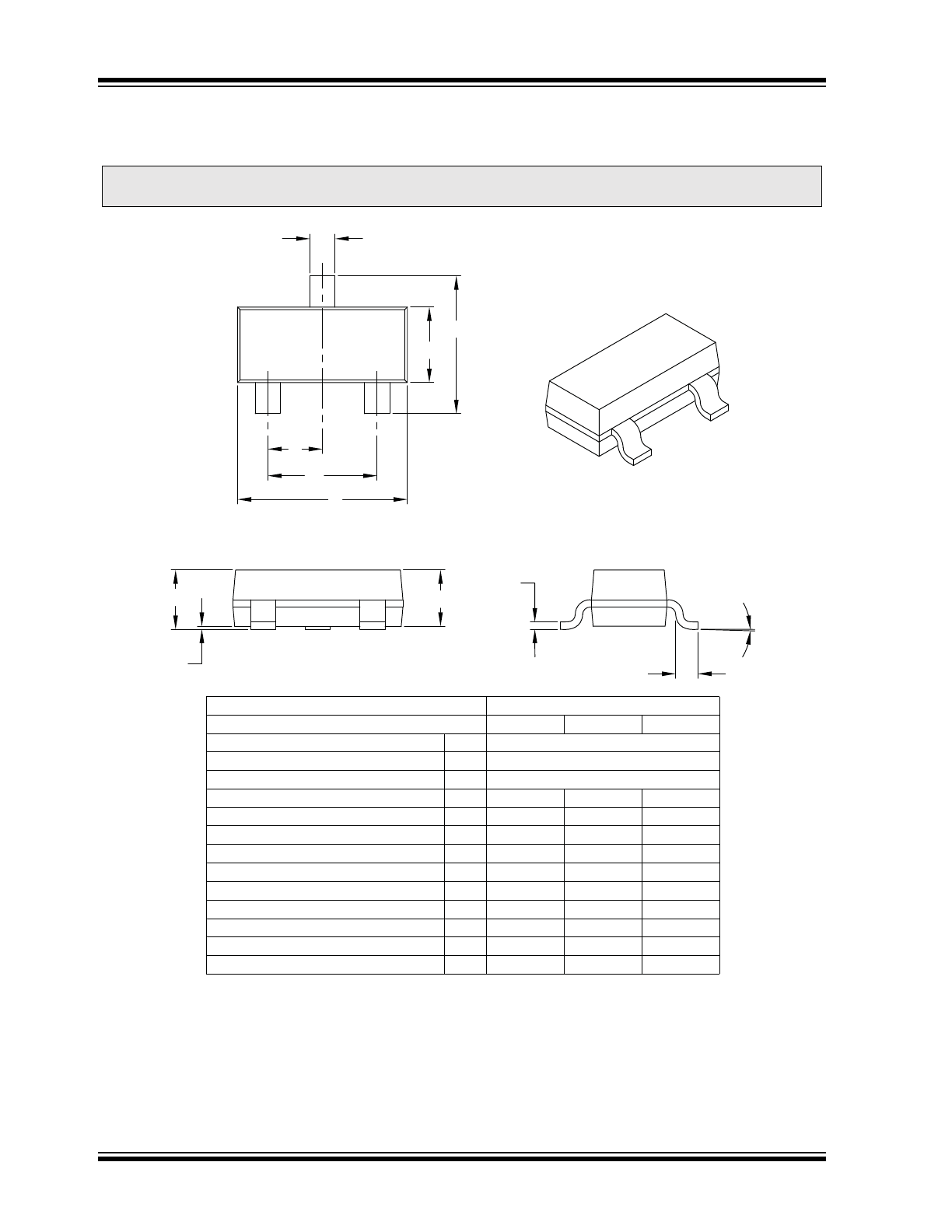
3-Lead Plastic Small Outline Transistor (TT or NB) [SOT-23]
Notes:
1. Dimensions D and E1 do not include mold flash or protrusions. Mold flash or protrusions shall not exceed 0.25 mm per side.
2. Dimensioning and tolerancing per ASME Y14.5M.
BSC: Basic Dimension. Theoretically exact value shown without tolerances.
Note:
For the most current package drawings, please see the Microchip Packaging Specification located at
http://www.microchip.com/packaging
Units
MILLIMETERS
Dimension Limits
MIN
NOM
MAX
Number of Pins
N
3
Lead Pitch
e
0.95 BSC
Outside Lead Pitch
e1
1.90 BSC
Overall Height
A
0.89
–
1.12
Molded Package Thickness
A2
0.79
0.95
1.02
Standoff
A1
0.01
–
0.10
Overall Width
E
2.10
–
2.64
Molded Package Width
E1
1.16
1.30
1.40
Overall Length
D
2.67
2.90
3.05
Foot Length
L
0.13
0.50
0.60
Foot Angle
φ
0°
–
10°
Lead Thickness
c
0.08
–
0.20
Lead Width
b
0.30
–
0.54
b
N
E
E1
2
1
e
e1
D
A
A1
A2
c
L
φ
Microchip Technology Drawing C04-104B

© 2007 Microchip Technology Inc.
DS21384D-page 9
TC1278/TC1279
PRODUCT IDENTIFICATION SYSTEM
To order or obtain information, e.g., on pricing or delivery, refer to the factory or the listed sales office
.
Device
TC1278:
3-Pin Reset Monitor for 5V Systems
TC1279:
3-Pin Reset Monitor for 5V Systems
Reset V
CC
Threshold:
5
= 4.625V
10
= 4.375V
15
= 4.125V
Temperature Range
E = -40
°C to +85°C
Package
NBTR
= Plastic Small Outline Transistor, (SOT23), 3-lead
(Tape and Reel)
PART NO.
X
XX
Package
Temperature
Range
Device
Examples:
a) TC1278-5ENBTR: 4.625
Reset
b) TC1278-10ENBTR: 4.375 Reset
c)
TC1278-15ENBTR: 4.125 Reset
a) TC1279-5ENBTR: 4.625
Reset
b) TC1279-10ENBTR: 4.375 Reset
c)
TC1279-15ENBTR: 4.125 Reset
-XX
Reset V
CC
Threshold

TC1278/TC1279
DS21384D-page 10
© 2007 Microchip Technology Inc.
NOTES: