
© 2007 Microchip Technology Inc.
DS21383C-page 1
TC1275/TC1276/TC1277
Features
• Precision V
CC
Monitor for 3.3V Systems
• 100 ms Minimum RESET, RESET Output
Duration
• Output Valid to V
CC
= 1.2V
• V
CC
Transient Immunity
• Small 3-Pin SOT-23 Package
• No External Components
Applications
• Computers
• Embedded Systems
• Battery Powered Equipment
• Critical µP Power Supply Monitoring
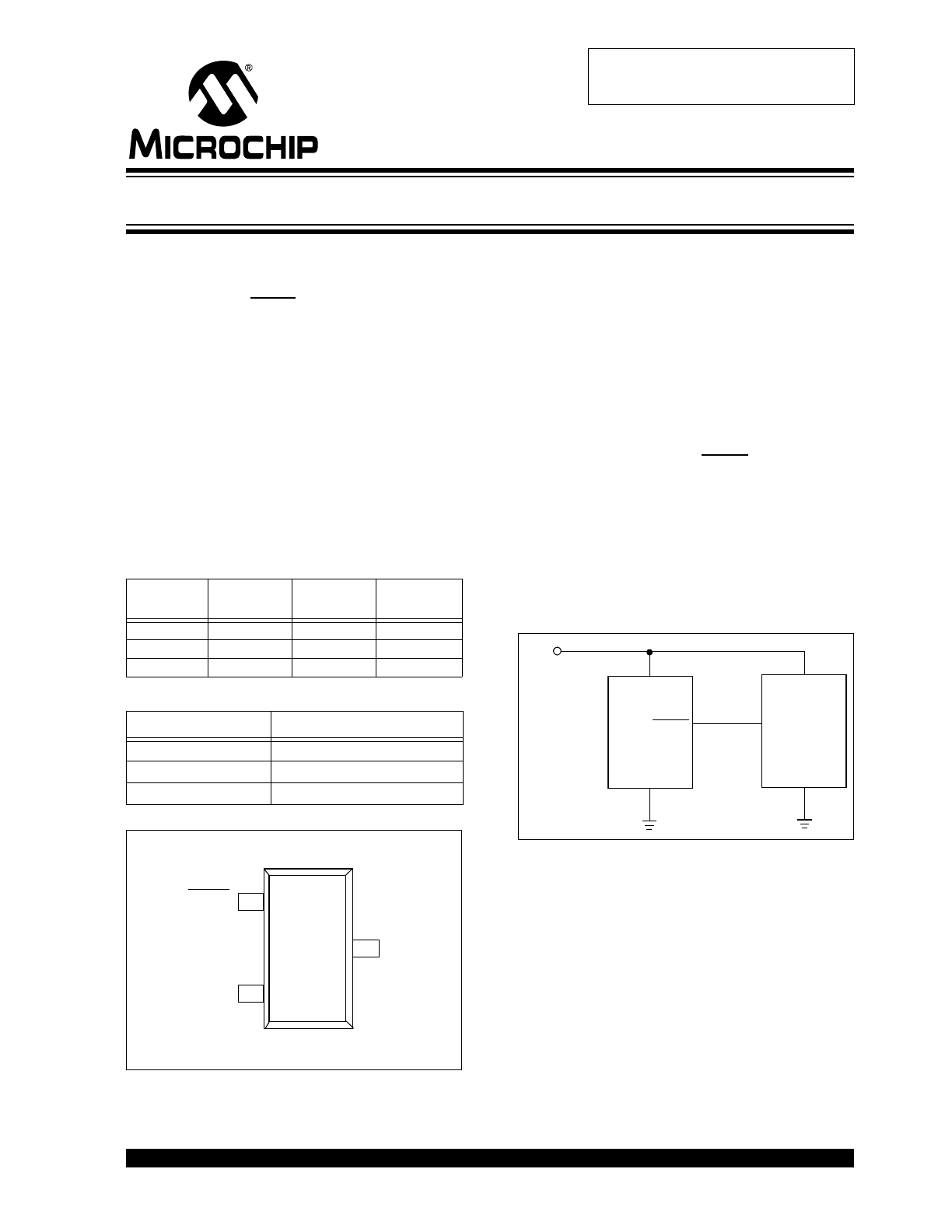
Device Selection Table
NOTE: “x” denotes a suffix for V
CC
threshold (see table below).
Package Type
General Description
The TC1275/TC1276/TC1277 are cost-effective
system supervisor circuits designed to monitor V
CC
in
digital systems and provide a reset signal to the host
processor when necessary. No external components
are required.
The reset output is driven active within 20 µs of V
CC
falling through the reset voltage threshold. RESET is
maintained active for a minimum of 100 ms after V
CC
rises above the reset threshold. The TC1277 has an
active-high RESET output while the TC1275 and
TC1276 have an active-low RESET output. TC1275
and TC1277 each have a complimentary output while
the TC1276 has an open drain output. The output of the
TC1275 and TC1276 is valid down to V
CC
= 1.2V. The
TC1277 is valid down to V
CC
= 1.8V. All three devices
are available in a 3-Pin SOT-23 package.
The TC1275/TC1276/TC1277 devices are optimized to
reject fast transient glitches on the V
CC
line.
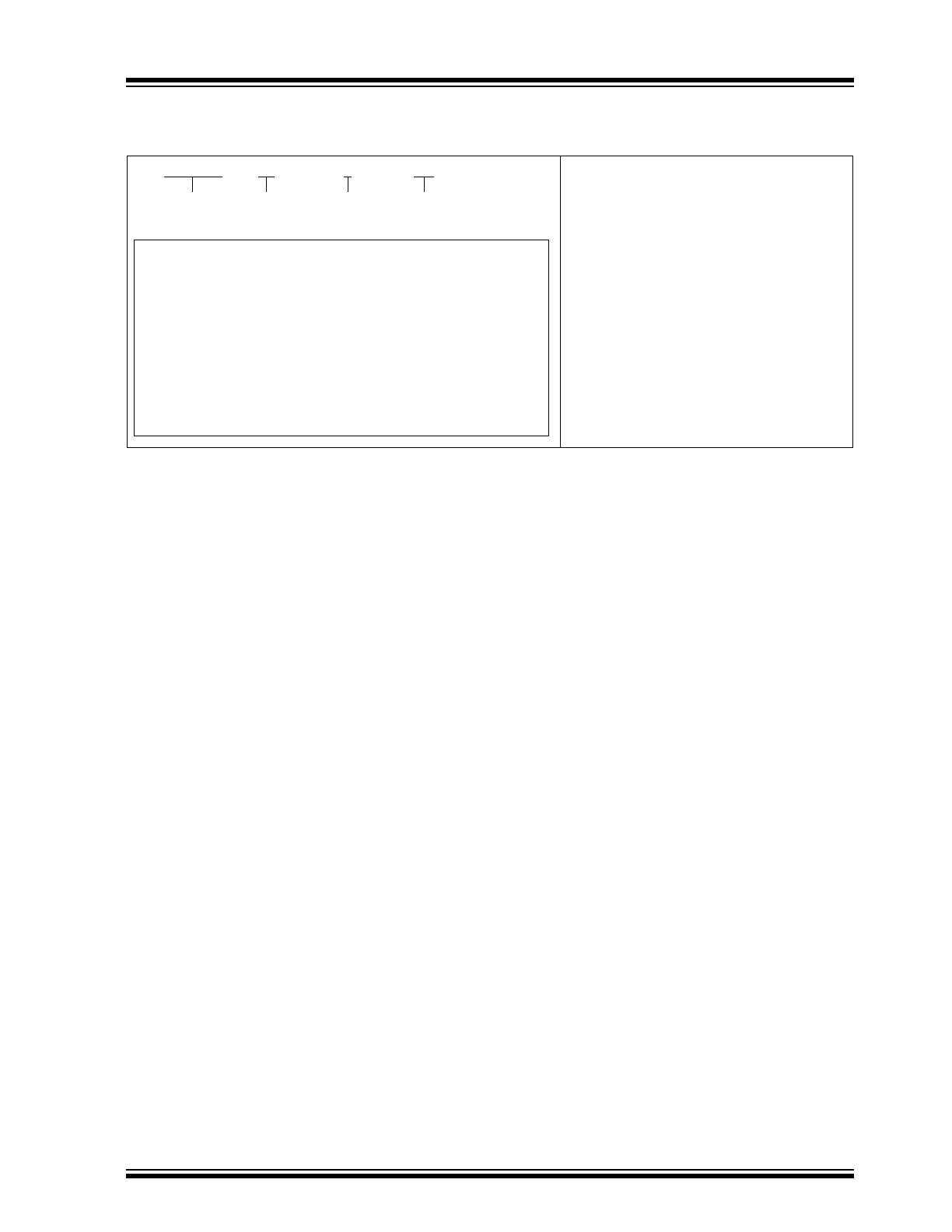
Typical Operating Circuit
Part
Number
Order
Package
Temp.
Range
TC1275-xENB Complimentary
3-Pin SOT-23
-40°C to +85°C
TC1276-xENB
Open-Drain
3-Pin SOT-23
-40°C to +85°C
TC1277-xENB Complimentary
3-Pin SOT-23
-40°C to +85°C
Suffix
Reset V
CC
Threshold (V)
5
3.06
10
2.88
20
2.55
V
CC
RESET
*(RESET)
GND
TC1275
TC1276
TC1277
1
2
3
*( ) is for TC1277
3-Pin SOT-23
TC1275
VCC
VCC
VCC
RESET
RESET
Input
GND
GND
Processor
1
2
3
3-Pin Reset Monitors for 3.3V Systems
Obsolete Device
TC1275/TC1276/TC1277
DS21383C-page 2
© 2007 Microchip Technology Inc.
1.0
ELECTRICAL
CHARACTERISTICS
Absolute Maximum Ratings*
Supply Voltage (V
CC
to GND) .............................+6.0V
RESET, RESET.......................... -0.3V to (V
CC
+ 0.3V)
Input Current, V
CC
..............................................20 mA
Output Current, RESET, RESET........................20 mA
Power Dissipation (T
A
≤ 70°C)
3-Pin SOT-23 (derate 4 mW/°C above +70°C)
................................................................230 mW
Operating Temperature Range.............-40°C to +85°C
Storage Temperature Range ..............-65°C to +150°C
*Stresses above those listed under "Absolute Maximum
Ratings" may cause permanent damage to the device. These
are stress ratings only and functional operation of the device
at these or any other conditions above those indicated in the
operation sections of the specifications is not implied.
Exposure to Absolute Maximum Rating conditions for
extended periods may affect device reliability.
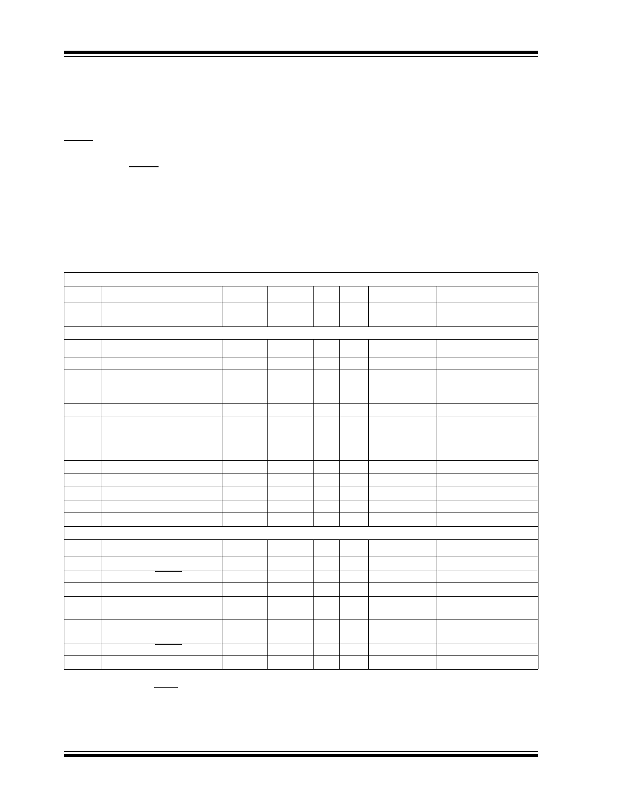
TC1275/TC1276/TC1277 ELECTRICAL SPECIFICATIONS
Recommended DC Operating Conditions: T
A
= -40°C to +85°C unless otherwise noted. Typical values are at T
A
= +25°C.
Symbol
Parameter
Min
Typ
Max
Units
Device
Test Conditions
V
CC
Supply Voltage
1.2
1.8
—
—
5.5
5.5
V
TC1275, TC1276
TC1277
Note 1
DC Electrical Characteristics: T
A
= -40°C to +85°C unless otherwise noted. Typical values are at T
A
= +25°C.
Symbol
Parameter
Min
Typ
Max
Units
Test Conditions
V
OH
Output Voltage @ 0-500
μA
V
CC
– 0.5V V
CC
– 0.1V
—
V
TC1275, TC1277 Note 1
I
OH
Output Current @ 2.4 Volts
V
CC
= 5V
V
CC
= 2.7V
—
—
13
1.3
—
—
mA
TC1275
TC1277
Note 2
I
OL
Output Current @ 0.4 Volts
+10
30
—
mA
Note 2, Note 5
I
CC
Operating Current
V
CC
< 5.5V
V
CCTP
< V
CC
< 5.5V
V
CC
< V
CCTP
—
—
—
20
20
350
35
35
700
µA
TC1275, TC1277
TC1276
TC1276
Note 3
Note 3
Note 3
V
CCTP-5
V
CC
Trip Point (TC1275/6/7-5)
2.98
3.06
3.15
V
Note 1
V
CCTP-10
V
CC
Trip Point (TC1275/6/7-10)
2.80
2.88
2.97
V
Note 1
V
CCTP-20
V
CC
Trip Point (TC1275/6/7-20)
2.47
2.55
2.64
V
Note 1
C
OUT
Output Capacitance
—
9
—
pF
R
P
Internal Pull-Up Resistor
3.0
6.0
9.0
k
Ω
TC1276
AC Electrical Characteristics: T
A
= -40°C to +85°C unless otherwise noted. Typical values are at T
A
= +25°C.
Symbol
Parameter
Min
Typ
Max
Units
Test Conditions
t
RST
RESET Active Time
100
200
300
ms
t
RPD1
V
CC
Detect to RESET
—
20
50
µs
TC1275, TC1276 V
CC(LOW)
= 1V,
Figure 3-2
t
RPD2
V
CC
Detect to RESET
—
20
50
µs
TC1277
V
CC(LOW)
= 1V,
Figure 3-4
t
F
V
CC
Slew Rate
(V
CCTP
(MAX) to V
CCTP
(MIN))
300
—
—
µs
Figure 3-2
,
Figure 3-4
t
R
V
CC
Slew Rate
(V
CCTP
(MIN) to V
CCTP
(MAX))
0
—
—
ns
Figure 3-1
,
Figure 3-3
t
RPU1
V
CC
Detect to RESET
100
200
300
ms
TC1275, TC1276 Note 4,
Figure 3-1
t
RPU2
V
CC
Detect to RESET
100
200
300
ms
TC1277
Note 4,
Figure 3-3
Note
1:
All voltages referenced to ground.
2:
Measured with V
CC
≥ 2.7 volts.
3:
Measured with RESET output open for TC1275/TC1276; measured with RESET output open for TC1277.
4:
t
R
= 5 µs.
5:
A 1 k
Ω external resistor may be required in some applications for proper operation of the microprocessor reset control circuit when using
the TC1276.
© 2007 Microchip Technology Inc.
DS21383C-page 3
TC1275/TC1276/TC1277
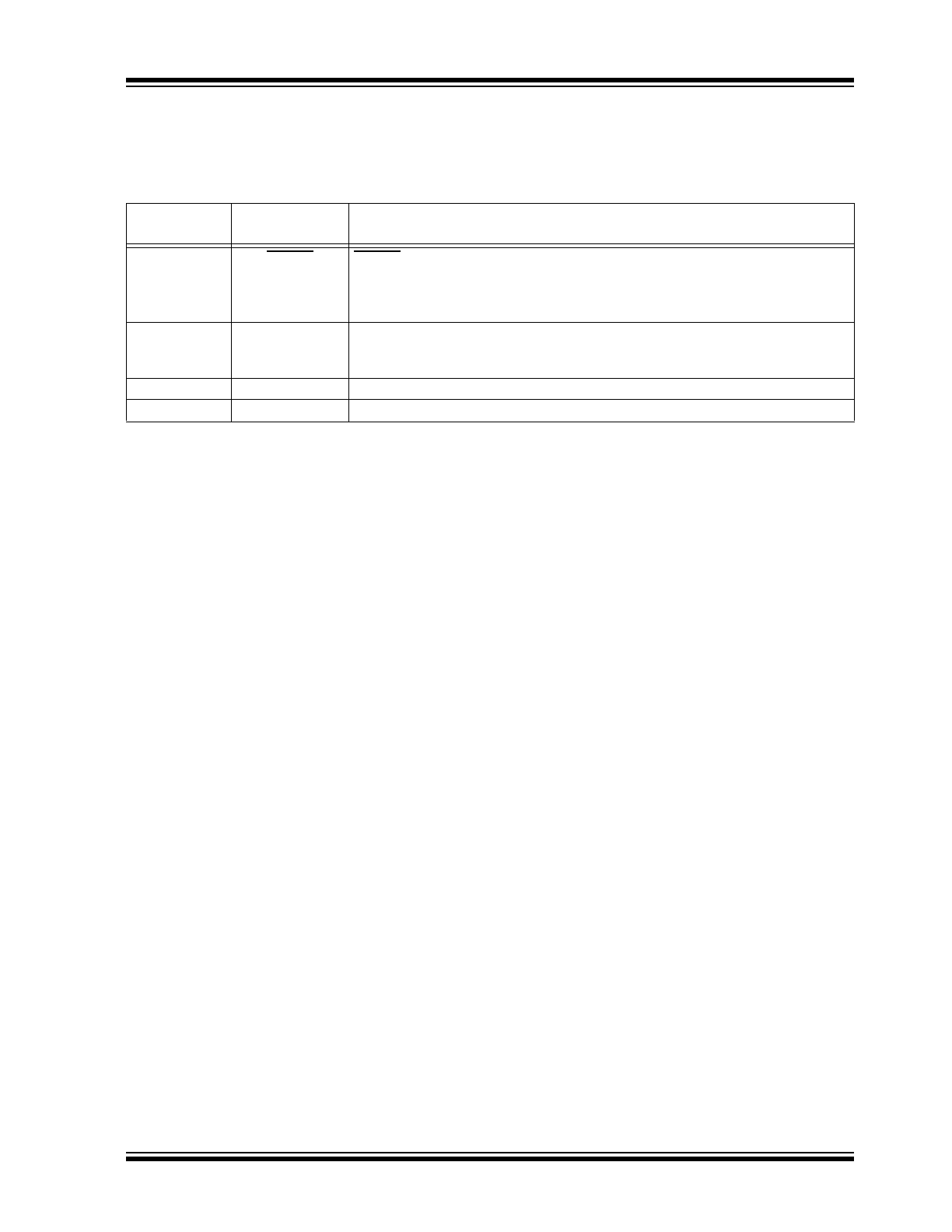
2.0
PIN DESCRIPTIONS
The descriptions of the pins are listed in Table 2-1.
TABLE 2-1:
PIN FUNCTION TABLE
Pin No.
(3-Pin SOT-23)
Symbol
Description
1
RESET
(TC1275/
TC1276)
RESET output remains low while V
CC
is below the reset voltage threshold, and
for 200 ms (100 ms minimum) after V
CC
rises above reset threshold. The output
stage of the TC1275 is complimentary. The output stage of the TC1276 is open-
drain.
1
RESET
(TC1277)
RESET output remains high while V
CC
is below the reset voltage threshold, and
for 200 ms (100 ms minimum) after V
CC
rises above reset threshold. The output
stage of the TC1277 is complimentary.
2
V
CC
Supply voltage (1.2V to 5.5V TC1275 and TC1276, 1.8V to 5.5V TC1277).
3
GND
Ground.
TC1275/TC1276/TC1277
DS21383C-page 4
© 2007 Microchip Technology Inc.
3.0
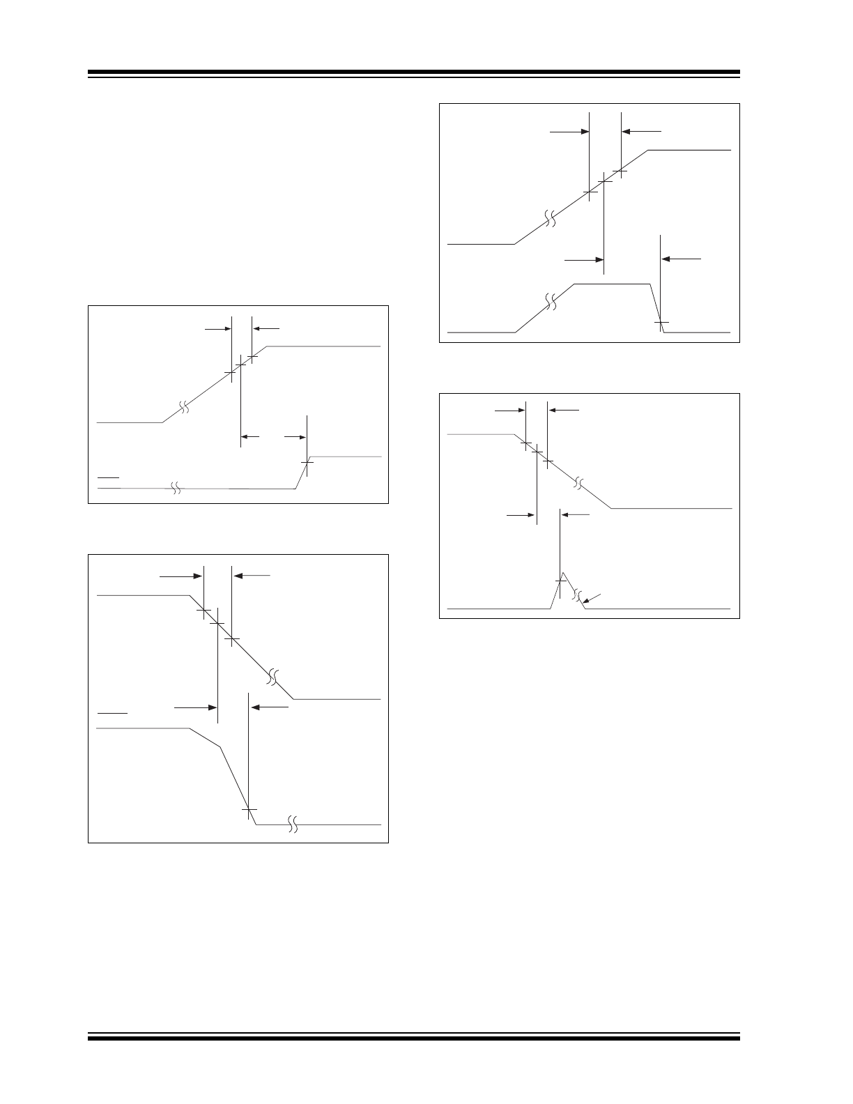
APPLICATIONS INFORMATION
3.1
Operation – Power Monitor
The TC1275/TC1276/TC1277 provide the function
of detecting out-of-tolerance power supply conditions
and warning a processor-based system of impending
power failure. When V
CC
is detected as out-of-
tolerance, the RESET signal is asserted. On power-up,
RESET is kept active for approximately 200 ms after
the power supply has reached the selected tolerance.
This allows the power supply and microprocessor to
stabilize before RESET is released.
FIGURE 3-1:
Timing Diagram – Power Up
(TC1275/TC1276).
FIGURE 3-2:
Timing Diagram – Power
Down (TC1275/TC1276).
FIGURE 3-3:
Timing Diagram –
Power Up (TC1277).
FIGURE 3-4:
Timing Diagram –
Power Down (TC1277).
V
CCTP
(MAX)
V
CCTP
(MIN)
t
R
V
CCTP
V
CC
RESET
t
RPU
1
V
OH
V
CC
RESET
V
CCTP
(MAX)
V
CCTP
V
CCTP
(MIN)
V
OL
t
RPD1
t
F
t
R
t
RPU2
V
OL
V
CCTP
V
CC
RESET
V
CCTP
(MAX)
V
CCTP
(MIN)
t
F
t
RPD2
V
CC
V
CCTP
(MAX)
V
OH
RESET
V
CCTP
V
CCTP
(MIN)
RESET SLEWS WITH V
CC
© 2007 Microchip Technology Inc.
DS21383C-page 5
TC1275/TC1276/TC1277
3.2
V
CC
Transient Rejection
The TC1275/TC1276/TC1277 provides accurate V
CC
monitoring and reset timing during power-up, power-
down, and brownout/sag conditions, and rejects
negative-going transients (glitches) on the power
supply line.
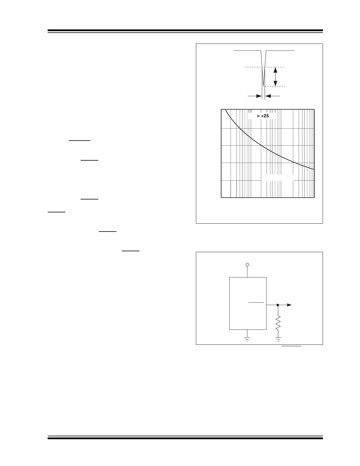
Figure 3-5
shows the maximum transient
duration vs. maximum negative excursion (overdrive)
for glitch rejection. Any combination of duration and
overdrive that lays under the curve will not generate a
reset signal. Combinations above the curve are
detected as a brownout or power-down. Transient
immunity can be improved by adding a capacitor in
close proximity to the V
CC
pin of the TC1275/TC1276/
TC1277.
3.3
RESET Signal Integrity During
Power-Down
The TC1275 RESET output is valid to V
CC
= 1.2V.
Below this voltage the output becomes an "open
circuit" and does not sink current. This means CMOS
logic inputs to the
μP will be floating at an undeter-
mined voltage. Most digital systems are completely
shut down well above this voltage. However, in situa-
tions where RESET must be maintained valid to
V
CC
= 0V, a pull-down resistor must be connected from
RESET to ground to discharge stray capacitances and
hold the output low (
Figure 3-6
). This resistor value,
though not critical, should be chosen such that it does
not appreciably load RESET under normal operation
(100 k
Ω will be suitable for most applications). Simi-
larly, a pull-up resistor to V
CC
is required for the
TC1277 to ensure a valid high RESET for V
CC
below
1.8V.
FIGURE 3-5:
Maximum Transient
Duration Vs. Overdrive For Glitch Rejection At
+25°C.
FIGURE 3-6:
ENSURING RESET VALID
TO V
CC
= 0V.
RESET COMPARATOR OVERDRIVE,
[
V
CCTP
- V
CC
]
(mV)
500
300
200
400
100
0
1
10
100
1000
MAXIMUM TRANSIENT DURATION (
μ
sec)
T
A
°
C
V
TH
Duration
Overdrive
V
CC
TC1275/6/7
TC1275
V
CC
V
CC
R1
100k
RESET
GND
TC1275/TC1276/TC1277
DS21383C-page 6
© 2007 Microchip Technology Inc.
4.0
TYPICAL CHARACTERISTICS
Note:
The graphs and tables provided following this note are a statistical summary based on a limited number of
samples and are provided for informational purposes only. The performance characteristics listed herein are
not tested or guaranteed. In some graphs or tables, the data presented may be outside the specified
operating range (e.g., outside specified power supply range) and therefore outside the warranted range.
V
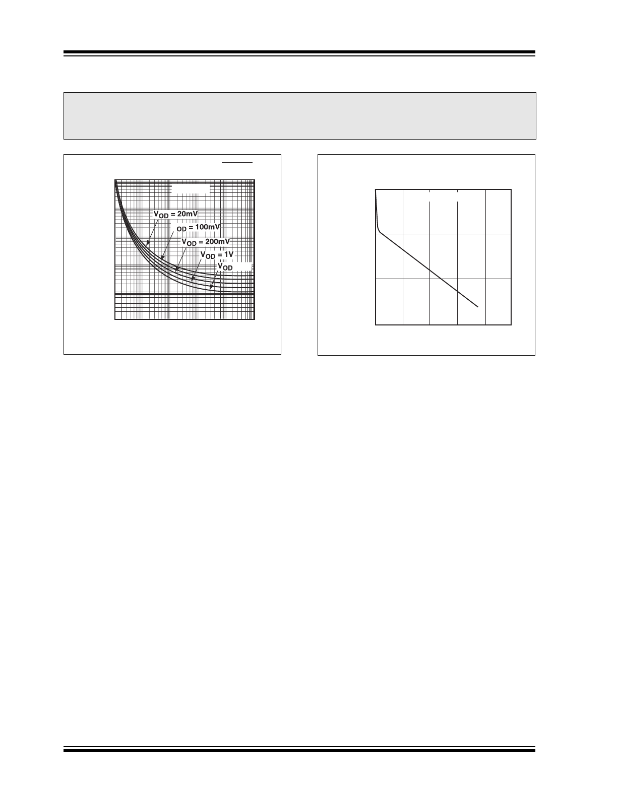
CC
SLEW RATE (V/
µsec)
V
CC
TO RESET DELAY (
µ
sec)
10000
1000
1
10
100
1000
10000
100000
100000
100
10
= 2V
V
T
A
= 25
°C
V
CC
Detect To RESET (RESET)
V
CC
TO RESET DELAY (
µ
sec)
300
200
100
0
0
1
2
3
4
5
COMPARATOR OVERDRIVE (V)
Reset Delays vs.
Comparator Overdrive
T
A
= 25
°C
© 2007 Microchip Technology Inc.
DS21383C-page 7
TC1275/TC1276/TC1277
5.0
PACKAGING INFORMATION
5.1
Package Marking Information
TC1275 (V)
Code
2.55
DA
2.88
DB
3.06
DC
TC1276 (V)
Code
2.55
EA
2.88
EB
3.06
EC
TC1277 (V)
Code
2.55
FA
2.88
FB
3.06
FC
1
&
= part number code + temperature range
2
and voltage
ex: 1275-20 =
D A
3
represents year and quarter code
4
represents production lot ID code
TC1275/TC1276/TC1277
DS21383C-page 8
© 2007 Microchip Technology Inc.
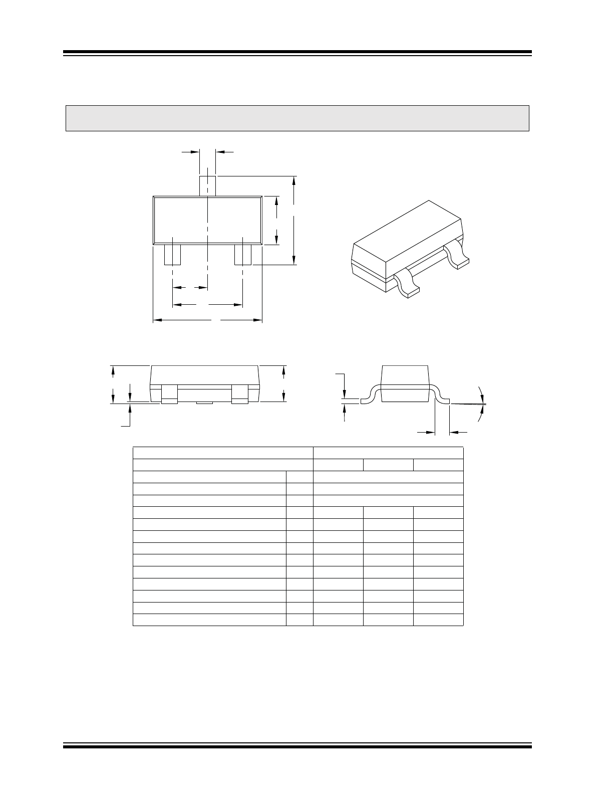
3-Lead Plastic Small Outline Transistor (TT or NB) [SOT-23]
Notes:
1. Dimensions D and E1 do not include mold flash or protrusions. Mold flash or protrusions shall not exceed 0.25 mm per side.
2. Dimensioning and tolerancing per ASME Y14.5M.
BSC: Basic Dimension. Theoretically exact value shown without tolerances.
Note:
For the most current package drawings, please see the Microchip Packaging Specification located at
http://www.microchip.com/packaging
Units
MILLIMETERS
Dimension Limits
MIN
NOM
MAX
Number of Pins
N
3
Lead Pitch
e
0.95 BSC
Outside Lead Pitch
e1
1.90 BSC
Overall Height
A
0.89
–
1.12
Molded Package Thickness
A2
0.79
0.95
1.02
Standoff
A1
0.01
–
0.10
Overall Width
E
2.10
–
2.64
Molded Package Width
E1
1.16
1.30
1.40
Overall Length
D
2.67
2.90
3.05
Foot Length
L
0.13
0.50
0.60
Foot Angle
φ
0°
–
10°
Lead Thickness
c
0.08
–
0.20
Lead Width
b
0.30
–
0.54
b
N
E
E1
2
1
e
e1
D
A
A1
A2
c
L
φ
Microchip Technology Drawing C04-104B
© 2007 Microchip Technology Inc.
DS21383C-page9
TC1275/TC1276/TC1277
PRODUCT IDENTIFICATION SYSTEM
To order or obtain information, e.g., on pricing or delivery, refer to the factory or the listed sales office.
PART NO.
X
/XX
Package
Temperature
Range
Device
Device:
TC1275: 3-Pin Reset Monitor - Complementary
TC1276: 3-Pin Reset Monitor - Open-Drain
TC1277: 3-Pin Reset Monitor - Complementary
Reset V
CC
Threshold Voltage
5
= 3.06V
10
= 2.88V
15
= 2.55V
Temperature Range:
E
= -40°C to +85°C
Package:
NB = Plastic Small Outline Transistor (SOT-23), 3-lead
Examples:
a)
TC1275
-10ENBTR:
2.88V Reset Monitor
b)
TC1275
-15ENBTR:
2.55V Reset Monitor
c)
TC1275
-5ENBTR:
3.06V Reset Monitor
a)
TC1276
-10ENBTR:
2.88V Reset Monitor
b)
TC1276
-15ENBTR:
2.55V Reset Monitor
c)
TC1276
-5ENBTR:
3.06V Reset Monitor
a)
TC1277
-10ENBTR:
2.88V Reset Monitor
b)
TC1277
-15ENBTR:
2.55V Reset Monitor
c)
TC1277
-5ENBTR:
3.06V Reset Monitor
XX
Reset V
CC
Threshold

TC1275/TC1276/TC1277
DS21383C-page 10
© 2007 Microchip Technology Inc.
NOTES: