
2012-2013 Microchip Technology Inc.
DS20002286C-page 1
MCP3911
Features
• Two Synchronous Sampling 16/24-bit Resolution
Delta-Sigma A/D Converters
• 94.5 dB SINAD, -106.5 dBc Total Harmonic
Distortion (THD) (up to 35
th
harmonic), 111 dB
SFDR for Each Channel
• 2.7V – 3.6V AV
DD
, DV
DD
• Programmable Data Rate up to 125 ksps
- 4 MHz Maximum Sampling Frequency
• Oversampling Ratio up to 4096
• Ultra Low Power Shutdown Mode with <2 µA
• -122 dB Crosstalk between the Two Channels
• Low Drift 1.2V Internal Voltage Reference: 7 ppm/°C
• Differential Voltage Reference Input Pins
• High Gain Programmable Gain Amplifier (PGA)
on Each Channel (up to 32V/V)
• Phase Delay Compensation with 1 µs Time
Resolution
• Separate Modulator Output Pins for Each
Channel
• Separate Data Ready Pin for Easy
Synchronization
• Individual 24-bit Digital Offset and Gain Error
Correction for Each Channel
• High-Speed 20 MHz SPI Interface with Mode 0,0
and 1,1 Compatibility
• Continuous Read/Write Modes for Minimum
Communication
• Low Power Consumption (8.9 mW at 3.3V,
5.6 mW at 3.3V in low-power mode, typical)
• Available in Small 20-lead QFN and SSOP
Packages, Pin-to-pin Compatible with MCP3901
• Extended Temperature Range: -40°C to +125°C
Applications
• Energy Metering and Power Measurement
• Automotive
• Portable Instrumentation
• Medical and Power Monitoring
• Audio/Voice Recognition
Description
The MCP3911 is a 2.7V to 3.6V dual channel Analog
Front End (AFE) containing two synchronous sampling
Delta-Sigma Analog-to-Digital Converters (ADC), two
PGAs, phase delay compensation block, low-drift
internal voltage reference, modulator output block,
digital offset and gain errors calibration registers and
high-speed 20 MHz SPI compatible serial interface.
The MCP3911 ADCs are fully configurable with
features such as: 16/24-bit resolution, OSR from 32 to
4096, gain from 1x to 32x, independent shutdown and
reset, dithering and auto-zeroing. The communication
is largely simplified with the one-byte-long commands
including various continuous read/write modes that can
be accessed by the Direct Memory Access (DMA) of an
MCU with a separate data ready pin that can be directly
connected to an Interrupt Request (IRQ) input of an
MCU.
The MCP3911 is capable of interfacing a large variety
of voltage and current sensors including shunts,
current transformers, Rogowski coils and Hall effect
sensors.
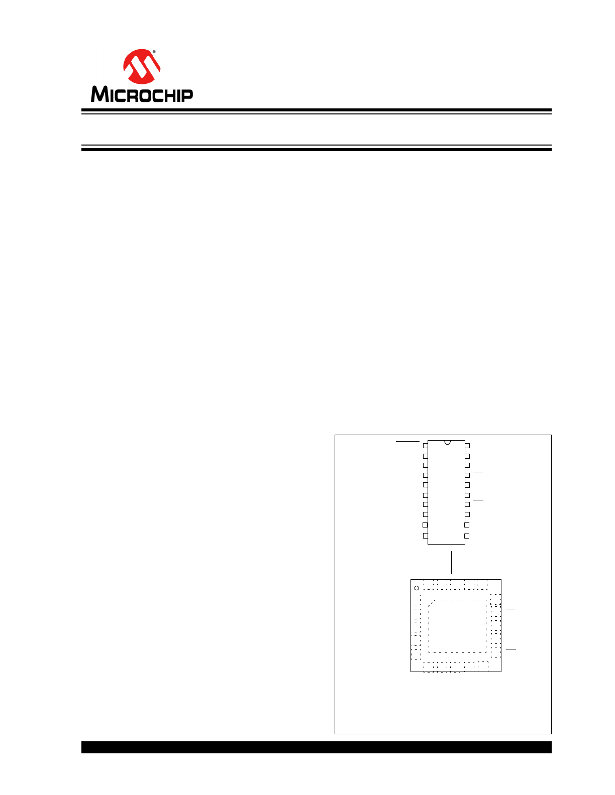
Package Type
OSC1/CLKI
1
2
3
4
20
19
18
17
16
15
14
13
5
6
7
8
OSC2
SDI
RESET
DV
DD
AV
DD
CH0+
CH0-
CH1-
12
9
D
GND
MDAT0
MDAT1
DR
CH1+
A
GND
SDO
11
10
REFIN+/OUT
REFIN-
CS
SCK
SDO
20-Lead
SSOP
20-Lead
4x4 QFN*
2
CH1-
CH1+
CH0+
SCK
CS
REFIN+/OUT
OSC2
REFIN
-
D
GND
MDA
T
1
OSC1/CLKI
AV
DD
DV
DD
RES
E
T
SD
I
CH0-
EP
20
1
19 18 17
3
4
14
13
12
11
6
7
8
9
21
5
10
15
16
A
GND
MDA
T
0
DR
*
Includes Exposed Thermal Pad (EP); see
Table 3-1
.
3.3V Two-Channel Analog Front End
MCP3911
DS20002286C-page 2
2012-2013 Microchip Technology Inc.
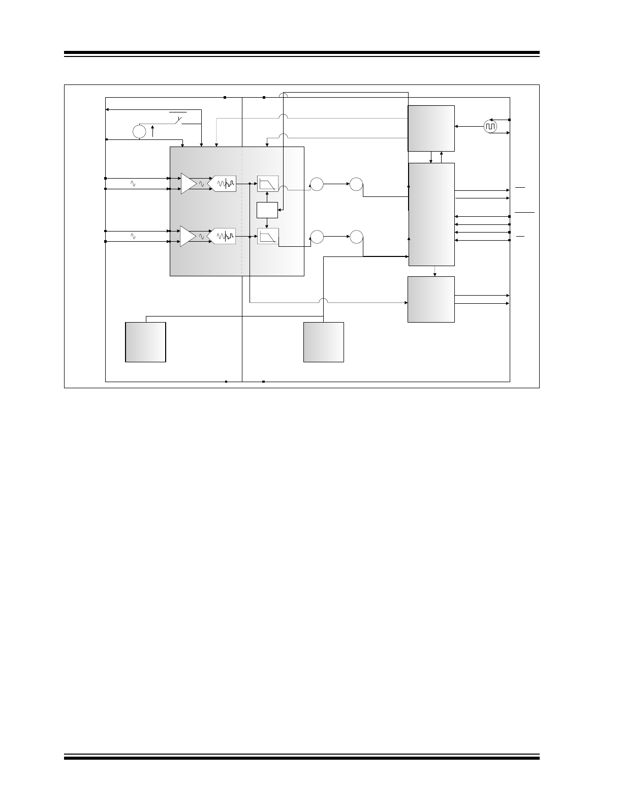
Functional Block Diagram
CH0+
CH0-
CH1+
CH1-
DUAL
'6ADC
ANALOG
DIGITAL
SINC
3
+
SINC
1
-
+
PGA
-
+
PGA
'6
Modulator
AMCLK
DMCLK/DRCLK
Phase
Shifter
)
PHASE <11:0>
DATA_CH0
<23:0>
MOD<7:0>
REFIN/OUT
REFIN-
AV
DD
A
GND
D
GND
DV
DD
MOD<3:0>
MOD<7:4>
POR
AV
DD
Monitoring
'6
Modulator
V
REF
+
V
REF
-
VREFEXT
Voltage
Reference
V
REF
+
-
POR
DV
DD
Monitoring
SDO
SDI
SCK
Xtal Oscillator
MCLK
OSC1
OSC2
DR
RESET
Digital SPI
Interface
Clock
Generation
Modulator
Output Block
MDAT1
MDAT0
DMCLK
OSR<2:0>
PRE<1:0>
MODOUT<1:0>
CS
+
OFFCAL_CH0
<23:0>
GAINCAL_CH0
<23:0>
X
+
OFFCAL_CH1
<23:0>
GAINCAL_CH1
<23:0>
X
DATA_CH1
<23:0>
SINC
3
+
SINC
1
2012-2013 Microchip Technology Inc.
DS20002286C-page 3
MCP3911
1.0
ELECTRICAL
CHARACTERISTICS
ABSOLUTE MAXIMUM RATINGS †
V
DD
..................................................................... -0.3V to 4.0V
Digital inputs and outputs w.r.t. A
GND
................ --0.3V to 4.0V
Analog input w.r.t. A
GND
..................................... ....-2V to +2V
V
REF
input w.r.t. A
GND
............................... -0.6V to V
DD
+0.6V
Storage temperature .....................................-65°C to +150°C
Ambient temp. with power applied ................-65°C to +125°C
Soldering temperature of leads (10 seconds) ............. +300°C
ESD on the analog inputs (HBM,MM) .................4.0 kV, 300V
ESD on all other pins (HBM,MM)........................4.0 kV, 300V
† Notice: Stresses above those listed under “Absolute
Maximum Ratings” may cause permanent damage to
the device. This is a stress rating only and functional
operation of the device at those or any other
conditions, above those indicated in the operational
listings of this specification, is not implied. Exposure to
maximum rating conditions for extended periods may
affect device reliability.
1.1
Electrical Specifications
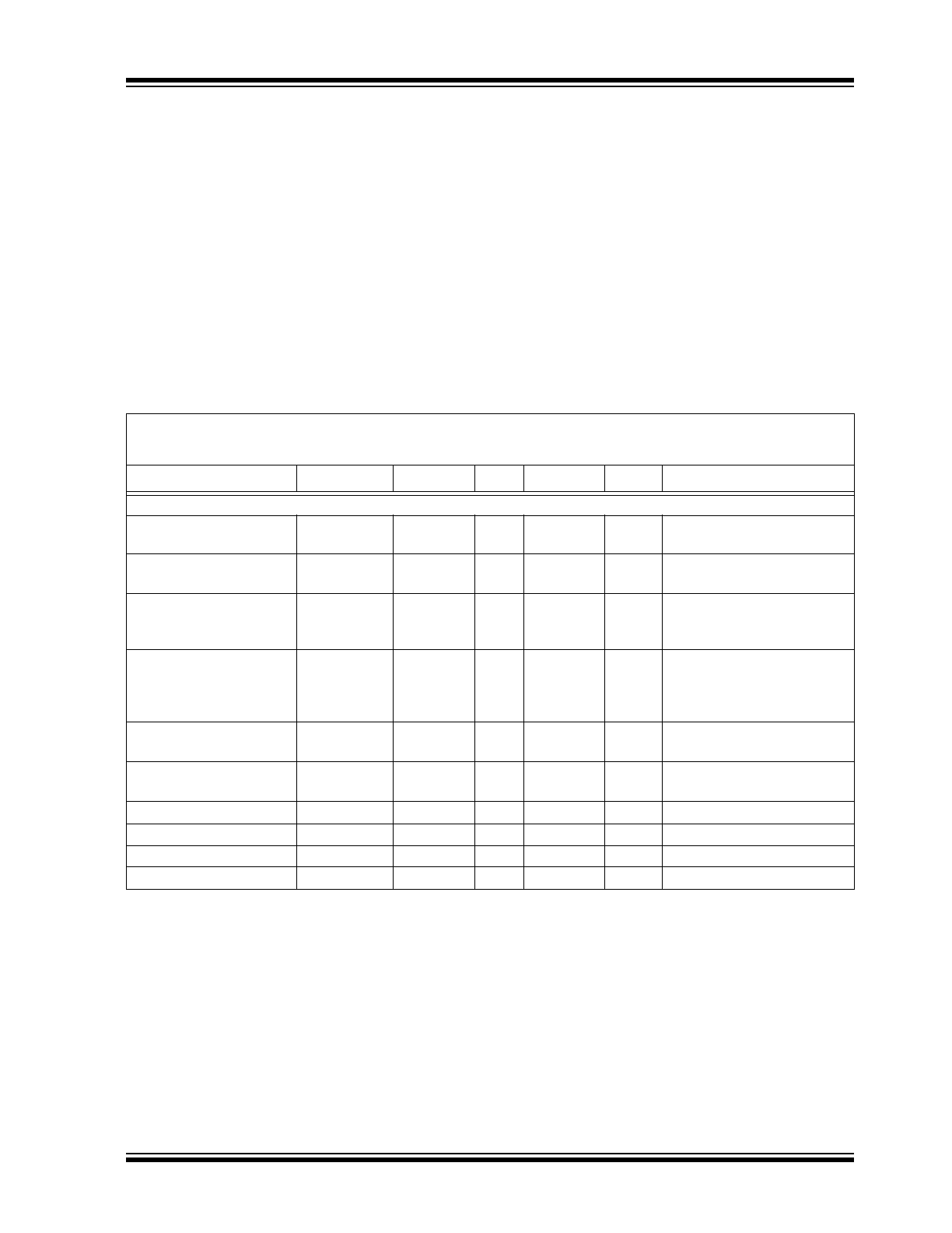
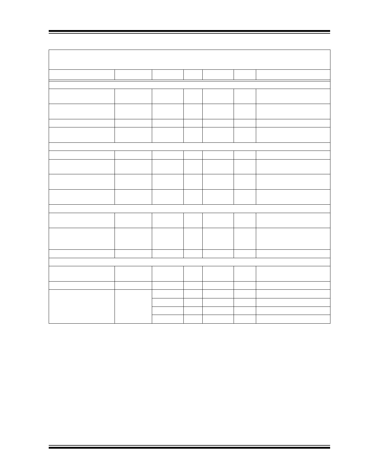
TABLE 1-1:
ANALOG SPECIFICATIONS TARGET TABLE
Electrical Specifications: Unless otherwise indicated, all parameters apply at AV
DD
=
DV
DD
= 2.7V to 3.6V, MCLK = 4 MHz;
PRE<1:0> = 00; OSR = 256; GAIN = 1; VREFEXT =
0
, CLKEXT =
1
, AZ_FREQ = 0, DITHER<1:0> = 11, BOOST<1:0> = 10;
V
CM
= 0V; T
A
= -40°C to +125°C; V
IN
= 1.2V
PP
= 424 mV
RMS
at 50/60 Hz on both channels.
Characteristic
Sym
Min
Typ
Max
Units
Conditions
ADC Performance
Resolution (No Missing
Codes)
24
—
—
bits
OSR = 256 or greater
Sampling Frequency
f
S
(DMCLK)
—
1
4
MHz
For maximum condition,
BOOST<1:0> = 11
Output Data Rate
f
D
(DRCLK)
—
4
125
ksps
For maximum condition,
BOOST<1:0> = 11,
OSR = 32
Analog Input
Absolute Voltage on
CH0+, CH0-, CH1+,
CH1- pins
CH0+/-
-1
+1
V
All analog input channels,
measured to A
GND
Analog Input
Leakage Current
I
IN
—
±1
—
nA
RESET<1:0> = 11,
MCLK running continuously
Differential Input
Voltage Range
(CH
n+
- CH
n-
) -600/GAIN
—
+600/
GAIN
mV
V
REF
= 1.2V,
proportional to V
REF
Offset Error
V
OS
-1
0.2
+1
mV
Note 4
Offset Error Drift
—
0.5
—
µV/°C
Gain Error
GE
-4
—
+4
%
Note 4
Gain Error Drift
—
1
—
ppm/°C
Note 1:
This specification implies that the ADC output is valid over this entire differential range and that there is no distortion or
instability across this input range. Dynamic Performance specified at -0.5 dB below the maximum signal range,
V
IN
= 1.2V
PP
= 424 mV
RMS
, V
REF
= 1.2V at 50/60 Hz. See
Section 4.0, Terminologies And Formulas
for definition.
This parameter is established by characterization and not 100% tested. See performance graphs for other than default
settings provided here.
2:
For these operating currents, the following configuration bit settings apply: SHUTDOWN<1:0> =
00
,
RESET<1:0> =
00
, VREFEXT =
0
, CLKEXT =
0
.
3:
For these operating currents, the following configuration bit settings apply: SHUTDOWN<1:0> =
11
, VREFEXT =
1
,
CLKEXT =
1
.
4:
Applies to all gains. Offset and gain errors depend on PGA gain setting, see
Section 2.0, Typical Performance
Curves
for typical performance.
5:
Outside of this range, the ADC accuracy is not specified. An extended input range of ±2 V can be applied continuously
to the part with no damage.
6:
For proper operation and optimizing ADC accuracy, AMCLK should be limited to the maximum frequency defined in
Table 5-2
as a function of the BOOST and PGA settings chosen. MCLK can take larger values as long as the prescaler
settings (PRE<1:0>) limit AMCLK = MCLK/PRESCALE in the defined range in
Table 5-2
.
MCP3911
DS20002286C-page 4
2012-2013 Microchip Technology Inc.
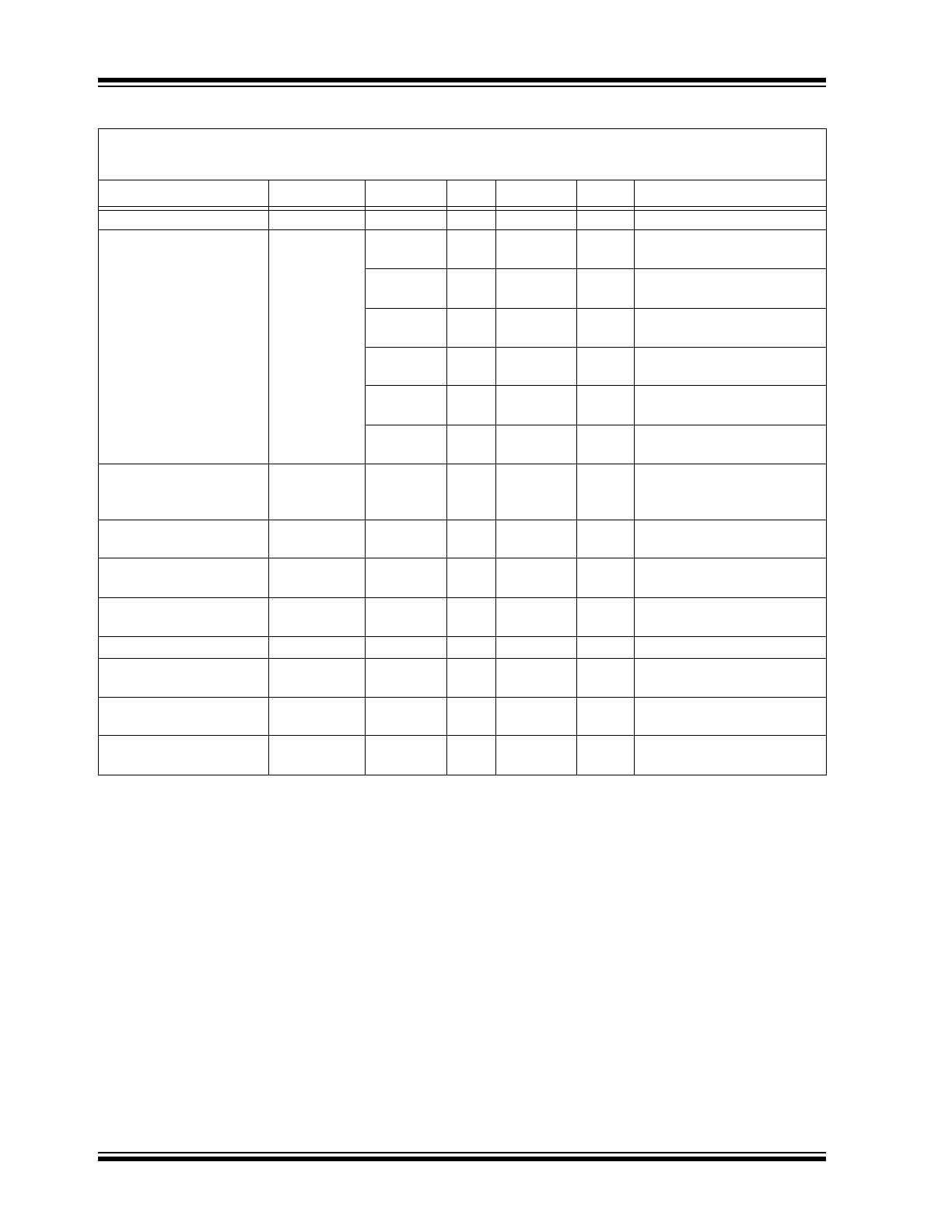
Integral Non-Linearity
INL
5
ppm
Differential Input
Impedance
Z
IN
232
—
—
k
Ω
G = 1,
proportional to 1/AMCLK
142
—
—
k
Ω
G = 2,
proportional to 1/AMCLK
72
—
—
k
Ω
G = 4,
proportional to 1/AMCLK
38
—
—
k
Ω
G = 8,
proportional to 1/AMCLK
36
—
—
k
Ω
G = 16,
proportional to 1/AMCLK
33
—
—
k
Ω
G = 32,
proportional to 1/AMCLK
Signal-to-Noise
and Distortion Ratio
(
Note 1
)
SINAD
92
94.5
—
dB
Total Harmonic Distortion
(
Note 1
)
THD
—
-106.5
-103
dBc
Includes the first
35 harmonics
Signal-to-Noise Ratio
(
Note 1
)
SNR
92
95
—
dB
Spurious Free
Dynamic Range (
Note 1
)
SFDR
—
111
—
dBFS
Crosstalk (50, 60 Hz)
CTALK
—
-122
—
dB
AC Power
Supply Rejection
AC PSRR
—
-73
—
dB
AV
DD
= DV
DD
= 3.3V+0.6V
PP
,
50/60 Hz, 100/120 Hz
DC Power
Supply Rejection
DC PSRR
—
-73
—
dB
AV
DD
= DV
DD
= 2.7V to 3.6V
DC Common Mode
Rejection
DC CMRR
—
-105
—
dB
V
CM
from -1V to +1V
TABLE 1-1:
ANALOG SPECIFICATIONS TARGET TABLE (CONTINUED)
Electrical Specifications: Unless otherwise indicated, all parameters apply at AV
DD
=
DV
DD
= 2.7V to 3.6V, MCLK = 4 MHz;
PRE<1:0> = 00; OSR = 256; GAIN = 1; VREFEXT =
0
, CLKEXT =
1
, AZ_FREQ = 0, DITHER<1:0> = 11, BOOST<1:0> = 10;
V
CM
= 0V; T
A
= -40°C to +125°C; V
IN
= 1.2V
PP
= 424 mV
RMS
at 50/60 Hz on both channels.
Characteristic
Sym
Min
Typ
Max
Units
Conditions
Note 1:
This specification implies that the ADC output is valid over this entire differential range and that there is no distortion or
instability across this input range. Dynamic Performance specified at -0.5 dB below the maximum signal range,
V
IN
= 1.2V
PP
= 424 mV
RMS
, V
REF
= 1.2V at 50/60 Hz. See
Section 4.0, Terminologies And Formulas
for definition.
This parameter is established by characterization and not 100% tested. See performance graphs for other than default
settings provided here.
2:
For these operating currents, the following configuration bit settings apply: SHUTDOWN<1:0> =
00
,
RESET<1:0> =
00
, VREFEXT =
0
, CLKEXT =
0
.
3:
For these operating currents, the following configuration bit settings apply: SHUTDOWN<1:0> =
11
, VREFEXT =
1
,
CLKEXT =
1
.
4:
Applies to all gains. Offset and gain errors depend on PGA gain setting, see
Section 2.0, Typical Performance
Curves
for typical performance.
5:
Outside of this range, the ADC accuracy is not specified. An extended input range of ±2 V can be applied continuously
to the part with no damage.
6:
For proper operation and optimizing ADC accuracy, AMCLK should be limited to the maximum frequency defined in
Table 5-2
as a function of the BOOST and PGA settings chosen. MCLK can take larger values as long as the prescaler
settings (PRE<1:0>) limit AMCLK = MCLK/PRESCALE in the defined range in
Table 5-2
.
2012-2013 Microchip Technology Inc.
DS20002286C-page 5
MCP3911
Internal Voltage Reference
Tolerance
V
REF
1.176
1.2
1.224
V
VREFEXT = 0,
T
A
= +25°C only
Temperature Coefficient
TCV
REF
—
7
—
ppm/°C T
A
= -40°C to +125°C,
VREFEXT = 0
Output Impedance
ZOUTV
REF
—
2
—
k
Ω
VREFEXT = 0
Internal Voltage Refer-
ence Operating Current
AI
DD
V
REF
—
25
—
µA
VREFEXT = 0,
SHUTDOWN<1:0> = 11
Voltage Reference Input
Input Capacitance
—
—
10
pF
Differential Input Voltage
Range (V
REF
+ – V
REF
-)
V
REF
1.1
—
1.3
V
VREFEXT = 1
Absolute Voltage on
REFIN+ pin
V
REF+
V
REF
- + 1.1
—
V
REF
-
+ 1.3
V
VREFEXT = 1
Absolute Voltage on
REFIN- pin
V
REF-
-0.1
—
+0.1
V
REFIN- should be connected
to A
GND
when VREFEXT = 0
Master Clock Input
Master Clock Input
Frequency Range
f
MCLK
—
20
MHz
CLKEXT = 1,
Note 6
Crystal Oscillator
Operating Frequency
Range
f
XTAL
1
—
20
MHz
CLKEXT = 0,
Note 6
Analog Master Clock
AMCLK
—
—
16
MHz
Note 6
Power Supply
Operating Voltage, Ana-
log
AV
DD
2.7
—
3.6
V
Operating Voltage, Digital
DV
DD
2.7
—
3.6
V
Operating Current,
Analog (
Note 2
)
I
DD,A
—
1.5
2.3
mA
BOOST<1:0> = 00
—
1.8
2.8
mA
BOOST<1:0> = 01
—
2.5
3.5
mA
BOOST<1:0> = 10
—
4.4
6.25
mA
BOOST<1:0> = 11
TABLE 1-1:
ANALOG SPECIFICATIONS TARGET TABLE (CONTINUED)
Electrical Specifications: Unless otherwise indicated, all parameters apply at AV
DD
=
DV
DD
= 2.7V to 3.6V, MCLK = 4 MHz;
PRE<1:0> = 00; OSR = 256; GAIN = 1; VREFEXT =
0
, CLKEXT =
1
, AZ_FREQ = 0, DITHER<1:0> = 11, BOOST<1:0> = 10;
V
CM
= 0V; T
A
= -40°C to +125°C; V
IN
= 1.2V
PP
= 424 mV
RMS
at 50/60 Hz on both channels.
Characteristic
Sym
Min
Typ
Max
Units
Conditions
Note 1:
This specification implies that the ADC output is valid over this entire differential range and that there is no distortion or
instability across this input range. Dynamic Performance specified at -0.5 dB below the maximum signal range,
V
IN
= 1.2V
PP
= 424 mV
RMS
, V
REF
= 1.2V at 50/60 Hz. See
Section 4.0, Terminologies And Formulas
for definition.
This parameter is established by characterization and not 100% tested. See performance graphs for other than default
settings provided here.
2:
For these operating currents, the following configuration bit settings apply: SHUTDOWN<1:0> =
00
,
RESET<1:0> =
00
, VREFEXT =
0
, CLKEXT =
0
.
3:
For these operating currents, the following configuration bit settings apply: SHUTDOWN<1:0> =
11
, VREFEXT =
1
,
CLKEXT =
1
.
4:
Applies to all gains. Offset and gain errors depend on PGA gain setting, see
Section 2.0, Typical Performance
Curves
for typical performance.
5:
Outside of this range, the ADC accuracy is not specified. An extended input range of ±2 V can be applied continuously
to the part with no damage.
6:
For proper operation and optimizing ADC accuracy, AMCLK should be limited to the maximum frequency defined in
Table 5-2
as a function of the BOOST and PGA settings chosen. MCLK can take larger values as long as the prescaler
settings (PRE<1:0>) limit AMCLK = MCLK/PRESCALE in the defined range in
Table 5-2
.
MCP3911
DS20002286C-page 6
2012-2013 Microchip Technology Inc.
1.2
Serial Interface Characteristics
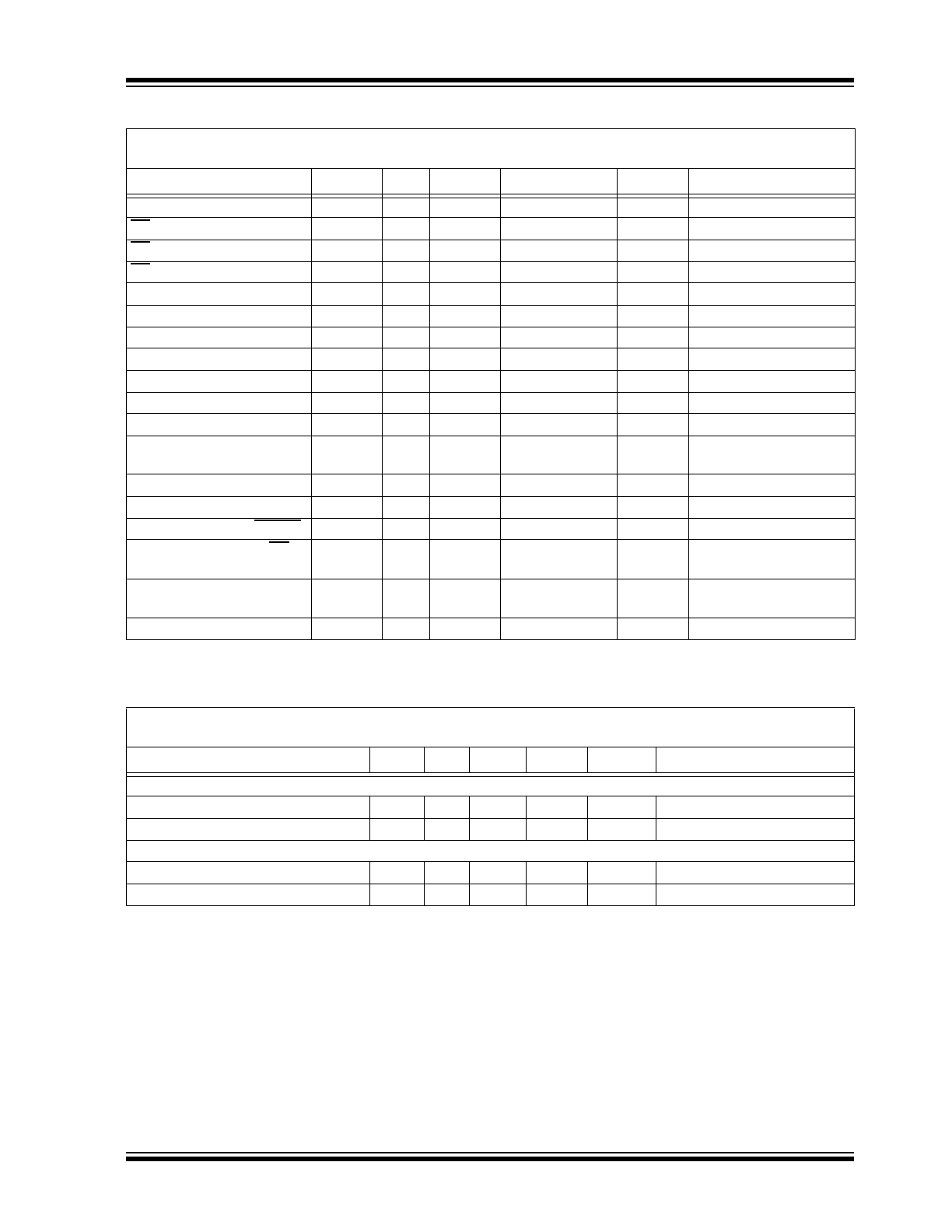
Operating Current, Digital
I
DD,D
—
0.2
0.3
mA
MCLK = 4 MHz,
proportional to MCLK
—
0.7
—
mA
MCLK = 16 MHz,
proportional to MCLK
Shutdown Current, Ana-
log
I
DDS,A
—
—
1
µA
AV
DD
pin only (
Note 3
)
Shutdown Current, Digital
I
DDS,D
—
—
1
µA
DV
DD
pin only (
Note 3
)
TABLE 1-2:
SERIAL DC CHARACTERISTICS TABLE
Electrical Specifications: Unless otherwise indicated, all parameters apply at DV
DD
= 2.7 to 3.6V,
T
A
= -40°C to +125°C, C
LOAD
= 30 pF, applies to all digital I/O.
Characteristics
Sym
Min
Typ
Max
Units
Test Conditions
High-level Input Voltage
V
IH
0.7 DV
DD
—
V
Schmitt Triggered
Low-level Input Voltage
V
IL
—
—
0.3 DV
DD
V
Schmitt Triggered
Input Leakage Current
I
LI
—
—
±1
µA
CS = DV
DD
,
V
IN
= D
GND
to DV
DD
Output leakage Current
I
LO
—
—
±1
µA
CS = DV
DD
,
V
OUT
= D
GND
or DV
DD
Hysteresis
of Schmitt Trigger Inputs
V
HYS
—
200
—
mV
Note 2
, DV
DD
= 3.3V only
Low-level Output Voltage
V
OL
—
—
0.4
V
I
OL
= +2.1 mA, DV
DD
= 3.3V
High-level Output Voltage
V
OH
DV
DD
-0.5
—
—
V
I
OH
= -2.1 mA, DV
DD
= 3.3V
Internal Capacitance
(all inputs and outputs)
C
INT
—
—
7
pF
T
A
= +25°C, SCK = 1.0 MHz,
DV
DD
= 3.3V (
Note 1
)
Note 1: This parameter is periodically sampled and not 100% tested.
2: This parameter is established by characterization and not production tested.
TABLE 1-1:
ANALOG SPECIFICATIONS TARGET TABLE (CONTINUED)
Electrical Specifications: Unless otherwise indicated, all parameters apply at AV
DD
=
DV
DD
= 2.7V to 3.6V, MCLK = 4 MHz;
PRE<1:0> = 00; OSR = 256; GAIN = 1; VREFEXT =
0
, CLKEXT =
1
, AZ_FREQ = 0, DITHER<1:0> = 11, BOOST<1:0> = 10;
V
CM
= 0V; T
A
= -40°C to +125°C; V
IN
= 1.2V
PP
= 424 mV
RMS
at 50/60 Hz on both channels.
Characteristic
Sym
Min
Typ
Max
Units
Conditions
Note 1:
This specification implies that the ADC output is valid over this entire differential range and that there is no distortion or
instability across this input range. Dynamic Performance specified at -0.5 dB below the maximum signal range,
V
IN
= 1.2V
PP
= 424 mV
RMS
, V
REF
= 1.2V at 50/60 Hz. See
Section 4.0, Terminologies And Formulas
for definition.
This parameter is established by characterization and not 100% tested. See performance graphs for other than default
settings provided here.
2:
For these operating currents, the following configuration bit settings apply: SHUTDOWN<1:0> =
00
,
RESET<1:0> =
00
, VREFEXT =
0
, CLKEXT =
0
.
3:
For these operating currents, the following configuration bit settings apply: SHUTDOWN<1:0> =
11
, VREFEXT =
1
,
CLKEXT =
1
.
4:
Applies to all gains. Offset and gain errors depend on PGA gain setting, see
Section 2.0, Typical Performance
Curves
for typical performance.
5:
Outside of this range, the ADC accuracy is not specified. An extended input range of ±2 V can be applied continuously
to the part with no damage.
6:
For proper operation and optimizing ADC accuracy, AMCLK should be limited to the maximum frequency defined in
Table 5-2
as a function of the BOOST and PGA settings chosen. MCLK can take larger values as long as the prescaler
settings (PRE<1:0>) limit AMCLK = MCLK/PRESCALE in the defined range in
Table 5-2
.
2012-2013 Microchip Technology Inc.
DS20002286C-page 7
MCP3911
TABLE 1-3:
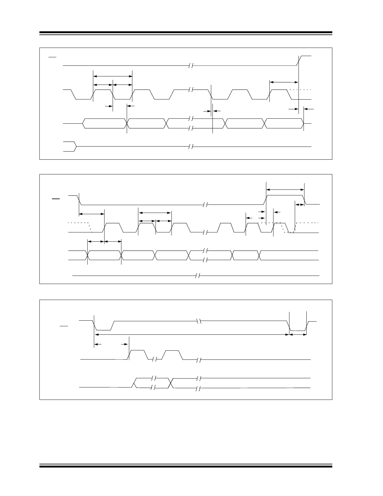
SERIAL AC CHARACTERISTICS TABLE
Electrical Specifications: Unless otherwise indicated, all parameters apply at DV
DD
= 2.7 to 3.6V,
T
A
= -40°C to +125°C, GAIN = 1, C
LOAD
= 30 pF.
Characteristics
Sym
Min
Typ
Max
Units
Test Conditions
Serial Clock frequency
f
SCK
—
—
20
MHz
CS setup time
t
CSS
25
—
—
ns
CS hold time
t
CSH
50
—
—
ns
CS disable time
t
CSD
50
—
—
ns
Data setup time
t
SU
5
—
—
ns
Data hold time
t
HD
10
—
—
ns
Serial Clock high time
t
HI
20
—
—
ns
Serial Clock low time
t
LO
20
—
—
ns
Serial Clock delay time
t
CLD
50
—
—
ns
Serial Clock enable time
t
CLE
50
—
—
ns
Output valid from SCK low
t
DO
—
—
25
ns
Modulator output
valid from AMCLK high
t
DOMDAT
—
—
1/(2 x AMCLK)
s
Output hold time
t
HO
0
—
—
ns
(
Note 1
)
Output disable time
t
DIS
—
—
25
ns
(
Note 1
)
Reset Pulse Width (RESET)
t
MCLR
100
—
—
ns
Data Transfer Time to DR
(Data Ready)
t
DODR
—
25
ns
(
Note 2
)
Modulator Mode Entry to
Modulator Data Present
t
MODSU
—
100
ns
Data Ready Pulse Low Time
t
DRP
1/DMCLK —
µs
Note 1: This parameter is periodically sampled and not 100% tested.
2: This parameter is established by characterization and not production tested.
TABLE 1-4:
TEMPERATURE SPECIFICATIONS TABLE
Electrical Specifications: Unless otherwise indicated, all parameters apply at AV
DD
= 2.7 to 3.6V, DV
DD
= 2.7 to
3.6V.
Parameters
Sym
Min
Typ
Max
Units
Conditions
Temperature Ranges
Operating Temperature Range
T
A
-40
—
+125
°C
Note 1
Storage Temperature Range
T
A
-65
—
+150
°C
Thermal Package Resistances
Thermal Resistance, 20L QFN
θ
JA
—
43
—
°C/W
Thermal Resistance, 20L SSOP
θ
JA
—
87.3
—
°C/W
Note 1: The internal junction temperature (T
J
) must not exceed the absolute maximum specification of +150°C.
MCP3911
DS20002286C-page 8
2012-2013 Microchip Technology Inc.
FIGURE 1-1:
Serial Output Timing Diagram.
FIGURE 1-2:
Serial Input Timing Diagram.
FIGURE 1-3:
Data Ready Pulse/Sampling Timing Diagram.
t
CSH
t
DIS
t
HI
t
LO
f
SCK
CS
SCK
SDO
MSB out
LSB out
SDI
Mode 1,1
Mode 0,0
t
HO
t
DO
DON’T CARE
CS
SCK
SDI
LSB in
MSB in
Mode 1,1
Mode 0,0
t
CSS
t
SU
t
HD
t
CSD
t
CSH
t
CLD
t
CLE
SDO
HI-Z
t
HI
t
LO
f
SCK
DR
SCK
t
DRP
SDO
1/f
D
t
DODR
2012-2013 Microchip Technology Inc.
DS20002286C-page 9
MCP3911
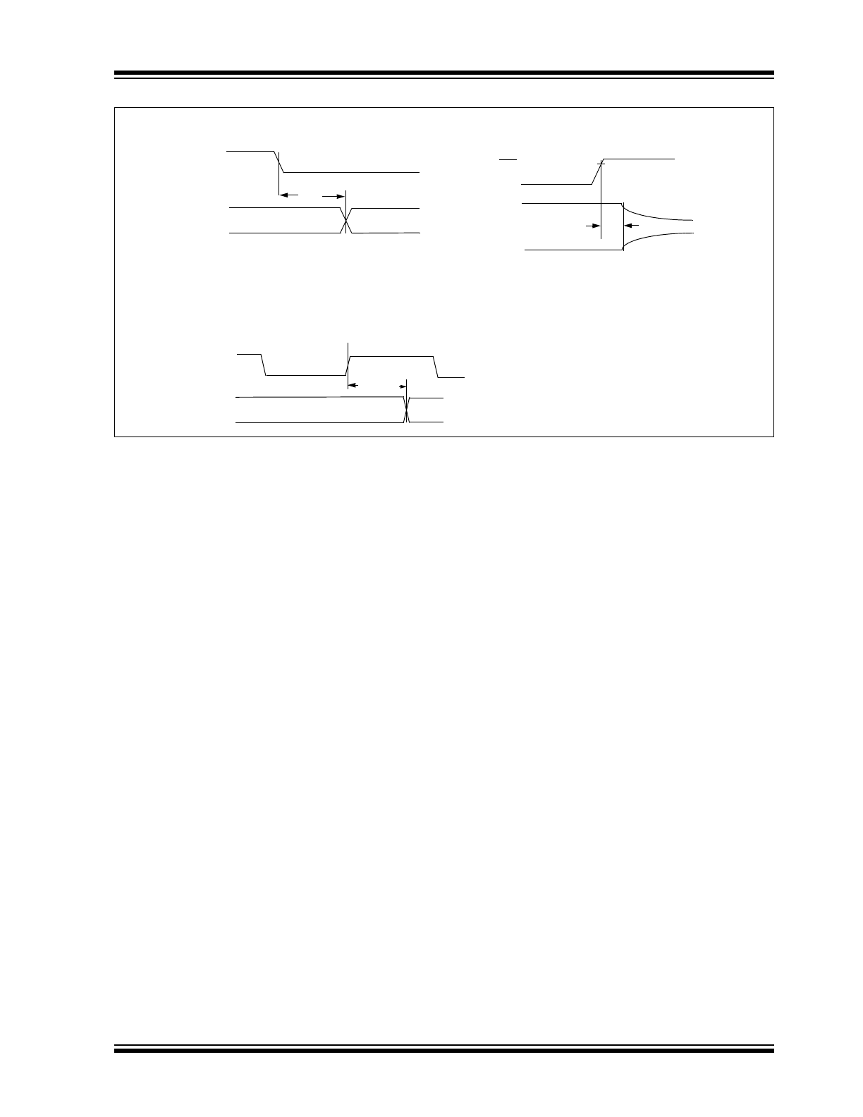
H
FIGURE 1-4:
Timing Diagrams (Continued).
CS
V
IH
Waveform for t
DIS
HI-Z
90%
10%
t
DIS
SDO
SCK
SDO
t
DO
Timing Waveform for t
DO
MDAT
OSC1/CLKI
Timing Waveform for MDAT0/1
Modulator Output Function
t
DOMDAT

MCP3911
DS20002286C-page 10
2012-2013 Microchip Technology Inc.
NOTES: