
2018 Microchip Technology Inc.
DS20005608A-page 1
SY89833AL
Features
• Ultra-Low Jitter Design:
- 80 fs
RMS
Additive Phase Jitter (typical)
• Guaranteed AC Performance Over Temperature
and Voltage:
- DC-to > 2 GHz throughput
- <470 ps Propagation Delay (IN-to-Q)
- <20 ps Within-Device Skew
- <190 ps Rise/Fall Times
• Unique Input Termination and V
T
Pin Accepts DC-
and AC-Coupled Inputs
• High-Speed LVDS Outputs
• 3.3V Power Supply Operation
• Industrial Temperature Range: –40°C to +85°C
• Available in 16-Pin (3 mm × 3 mm) QFN Package
Applications
• Processor Clock Distribution
• SONET Clock Distribution
• Fibre Channel Clock Distribution
• Gigabit Ethernet Clock Distribution
General Description
The SY89833AL is a lower noise version of the
SY89833L 3.3V, high-speed 2 GHz differential, low
voltage differential swing (LVDS) 1:4 fanout buffer
optimized for ultra-low skew applications. Within device
skew is guaranteed to be less than 20 ps over supply
voltage and temperature.
The differential input buffer has a unique internal
termination design that allows access to the
termination network through a V
T
pin. This feature
allows the device to easily interface to different logic
standards. A V
REF-AC
reference is included for
AC-coupled applications.
The SY89833AL is part of Microchip’s high-speed clock
synchronization family. For 2.5V applications, the
SY89832U provides similar functionality while
operating from a 2.5V ±5% supply. For applications that
require a different I/O combination, consult the
Microchip website and choose from a comprehensive
product line of high-speed, low-skew fanout buffers,
translators, and clock generators.
Package Type
SY89833AL
3x3 QFN (M)
13
14
15
16
12
11
10
9
1
2
3
4
8
7
6
5
Q1
/Q1
Q2
/Q2
IN
VT
VREF-AC
/IN
/Q0
Q0
VCC
GND
Q3
/Q3
VCC
EN
3.3V Low-Noise, Ultra-Precision 1:4 LVDS
Fanout Buffer/Translator with Internal Termination
United States Patent No. RE44,134
SY89833AL
DS20005608A-page 2
2018 Microchip Technology Inc.
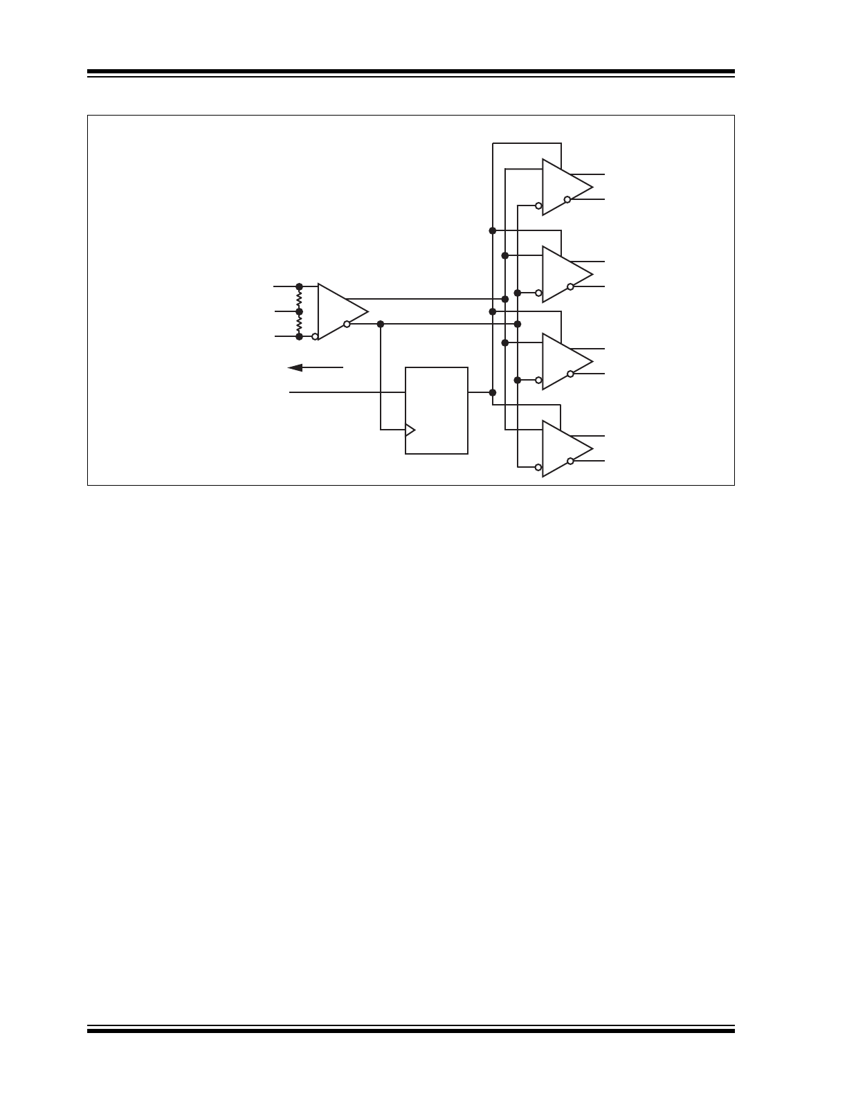
Functional Block Diagram
IN
/IN
D
Q
Q3
/Q3
Q2
/Q2
Q1
/Q1
Q0
/Q0
EN
(LVTTL/CMOS)
VT
50
50
VREF-AC
1:4

2018 Microchip Technology Inc.
DS20005608A-page 3
SY89833AL
1.0
ELECTRICAL CHARACTERISTICS
Absolute Maximum Ratings †
Supply Voltage (V
CC
) ................................................................................................................................ –0.5V to +4.0V
Input Voltage (V
IN
) ............................................................................................................................–0.5V to V
CC
+ 0.3V
LVDS Output Current (I
OUT
)..................................................................................................................................+10 mA
Input Current Source or Sink Current on (IN, /IN) .................................................................................................±50 mA
V
T
Current Source or Sink Current on (V
T
).........................................................................................................±100 mA
V
REF-AC
Current Source or Sink Current on (V
REF-AC
) ...........................................................................................±2 mA
Operating Ratings ‡
Supply Voltage Range .............................................................................................................................. +3.0V to +3.6V
†
Notice: Stresses above those listed under “Absolute Maximum Ratings” may cause permanent damage to the device.
This is a stress rating only and functional operation of the device at those or any other conditions above those indicated
in the operational sections of this specification is not intended. Exposure to maximum rating conditions for extended
periods may affect device reliability.
‡ Notice:
The device is not guaranteed to function outside its operating ratings.
SY89833AL
DS20005608A-page 4
2018 Microchip Technology Inc.
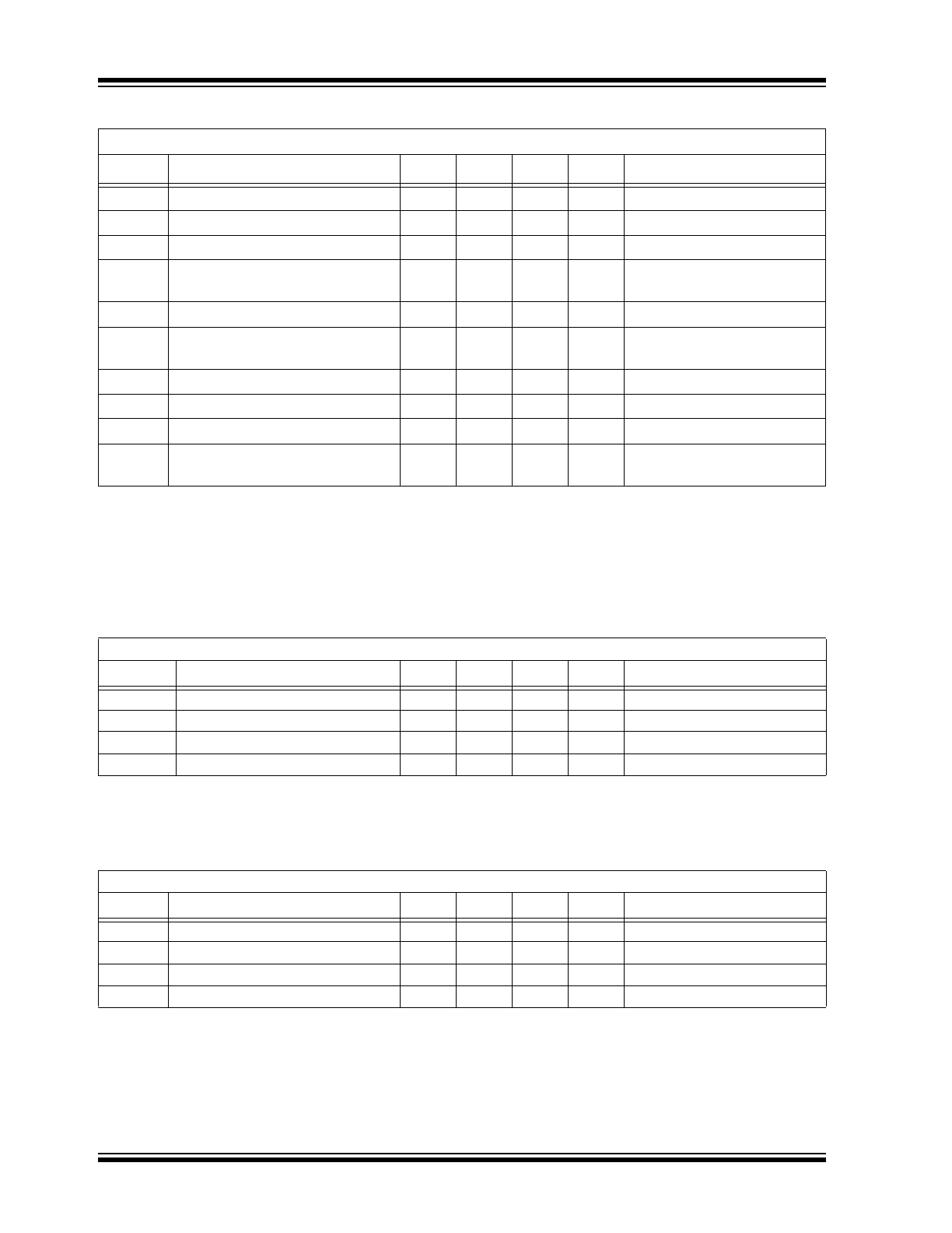
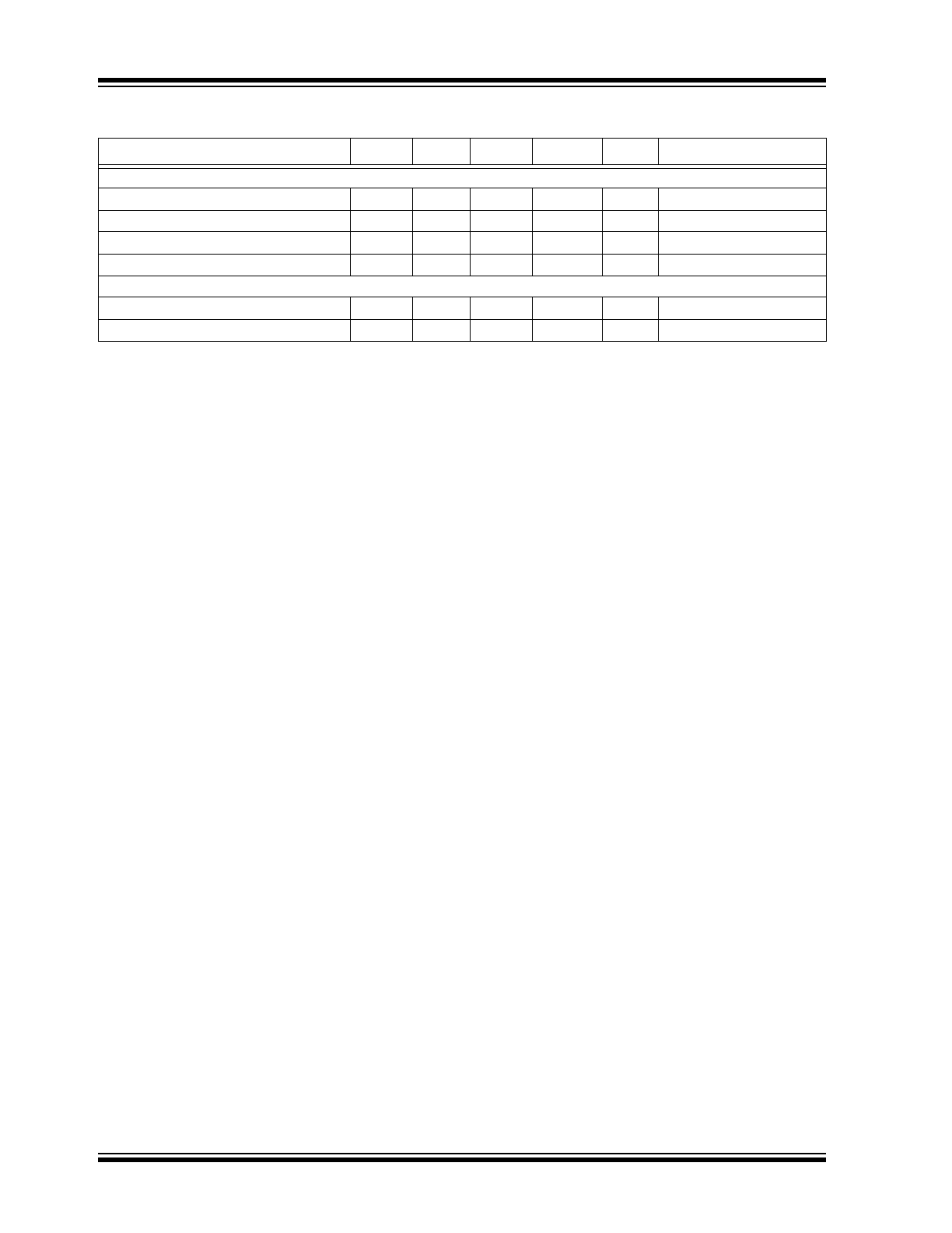
TABLE 1-1:
ELECTRICAL CHARACTERISTICS
Electrical Characteristics:
T
A
= –40°C to +85°C, unless otherwise stated. (
Note 1
)
.
Symbol
Parameters
Min.
Typ.
Max.
Units
Conditions
V
CC
Power Supply Voltage Range
3.0
3.3
3.6
V
—
I
CC
Power Supply Current
—
75
100
mA
No load; max. V
CC
R
IN
Input Resistance (IN-to-V
T
)
45
50
55
Ω
—
R
DIFF-IN
Differential Input Resistance
(IN-to-/IN)
90
100
110
Ω
—
V
IH
Input High Voltage (IN-to-/IN)
1.2
—
V
CC
V
—
V
IL
Input Low Voltage (IN-to-/IN)
0
—
V
IH
-
0.1
V
—
V
IN
Input Voltage Swing (IN-to-/IN)
0.1
—
1.7
V
See
Figure 5-3
V
DIFF_IN
Differential Input Voltage
0.2
—
—
V
See
Figure 5-4
|I
IN
|
Input Current (IN, /IN)
—
—
45
mA
Note 2
V
REF-AC
Reference Voltage
V
CC
-
1.525
V
CC
-
1.425
V
CC
-
1.325
V
—
Note 1:
The circuit is designed to meet the DC specifications shown in the above table after thermal equilibrium
has been established.
2:
Due to the internal termination (see "Input Buffer Structure" section) the input current depends on the
applied voltages at IN, /IN, and V
T
inputs. Do not apply a combination of voltages that causes the input
current to exceed the maximum limit.
TABLE 1-2:
LVDS OUTPUTS DC ELECTRICAL CHARACTERISTICS
Electrical Characteristics:
V
CC
= 3.3V ±10%, R
L
= 100Ω across the outputs; T
A
= –40°C to +85°C. (
Note 1
)
Symbol
Parameters
Min.
Typ.
Max.
Units
Conditions
V
OUT
Output Voltage Swing
250
325
—
mV
see
Figure 5-3
V
DIFF_OUT
Differential Output Voltage Swing
500
650
—
mV
see
Figure 5-4
V
OCM
Output Common-Mode Voltage
1.125
—
1.275
V
—
∆V
OCM
Change in Common-Mode Voltage
–50
—
50
mV
—
Note 1:
The circuit is designed to meet the DC specifications shown in the above table after thermal equilibrium
has been established.
TABLE 1-3:
LVTTL/CMOS DC ELECTRICAL CHARACTERISTICS
Electrical Characteristics:
V
CC
= 3.3V ±10%, T
A
= –40°C to +85°C. (
Note 1
)
Symbol
Parameters
Min.
Typ.
Max.
Units
Conditions
V
IH
Input High Voltage
2.0
—
V
CC
V
—
V
IL
Input Low Voltage
0
—
0.8
V
—
I
IH
Input High Current
–125
—
30
µA
—
I
IL
Input Low Current
–300
—
—
µA
—
Note 1:
The circuit is designed to meet the DC specifications shown in the above table after thermal equilibrium
has been established.
2018 Microchip Technology Inc.
DS20005608A-page 5
SY89833AL
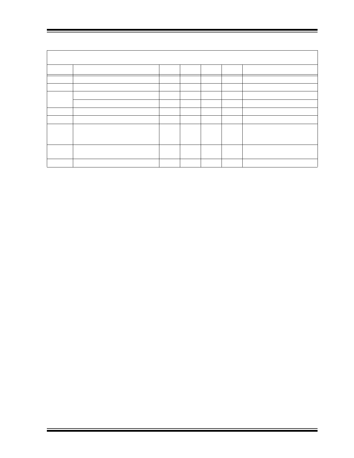
TABLE 1-4:
AC ELECTRICAL CHARACTERISTICS
Electrical Characteristics:
V
CC
= 3.3V ±10%, R
L
= 100Ω across the outputs; T
A
= –40°C to +85°C unless otherwise
stated. (
Note 1
)
Symbol
Parameters
Min.
Typ.
Max.
Units
Conditions
f
MAX
Maximum Frequency
2.0
—
—
GHz
V
OUT
≥ 200 mV
t
pd
Propagation Delay
250
—
470
ps
—
t
SKEW
Within-Device Skew
—
5
20
ps
Note 2
Part-to-Part Skew
—
—
200
ps
Note 3
t
S
Set-Up Time
400
—
—
ps
Note 4
t
H
Hold Time
400
—
—
ps
Note 4
t
JITTER
Additive Phase Jitter, RMS
—
80
—
fs
622.08 MHz @ 3.3V,
Integration range: 12 kHz to
20 MHz
t
r
/t
f
Output Rise/Fall Times (20% to
80%)
60
110
190
ps
At Full Output Swing
—
Duty Cycle
47
—
53
%
Differential I/O
Note 1:
High-frequency AC parameters are guaranteed by design and characterization.
2:
Within device skew is measured between two different outputs under identical input transitions.
3:
Part-to-part skew is defined for two parts with identical power supply voltages at the same temperature
and no skew at the edges at the respective inputs.
4:
Set-up and hold times apply to synchronous applications that intend to enable/disable before the next
clock cycle. For asynchronous applications, set-up and hold times do not apply.
SY89833AL
DS20005608A-page 6
2018 Microchip Technology Inc.
TEMPERATURE SPECIFICATIONS
Parameters
Sym.
Min.
Typ.
Max.
Units
Conditions
Temperature Ranges
Junction Operating Temperature
T
J
—
—
+125
°C
Note 1
Storage Temperature Range
T
S
–65
—
+150
°C
—
Lead Temperature
—
—
—
+260
°C
Soldering, 20s
Ambient Temperature
T
A
–40
—
+85
°C
—
Package Thermal Resistances (
Note 2
)
16-pin 3 mm x 3 mm QFN (Still-Air)
JA
—
60
—
°C/W
—
16-pin 3 mm x 3 mm QFN
Ψ
JB
—
33
—
°C/W
—
Note 1:
The maximum allowable power dissipation is a function of ambient temperature, the maximum allowable
junction temperature and the thermal resistance from junction to air (i.e., T
A
, T
J
,
JA
). Exceeding the
maximum allowable power dissipation will cause the device operating junction temperature to exceed the
maximum +125°C rating. Sustained junction temperatures above +125°C can impact the device reliability.
2:
Package thermal resistance assumes exposed pad is soldered (or equivalent) to the device's most nega-
tive potential on the PCB. Ψ
JB
and
JA
values are determined for a 4-layer board in still-air number, unless
otherwise stated.
2018 Microchip Technology Inc.
DS20005608A-page 7
SY89833AL
2.0
TYPICAL PERFORMANCE CURVES
V
CC
= 3.3V, GND = 0V, V
IN
= 400 mV, R
L
= 100Ω across the outputs; T
A
= +25°C unless otherwise stated.
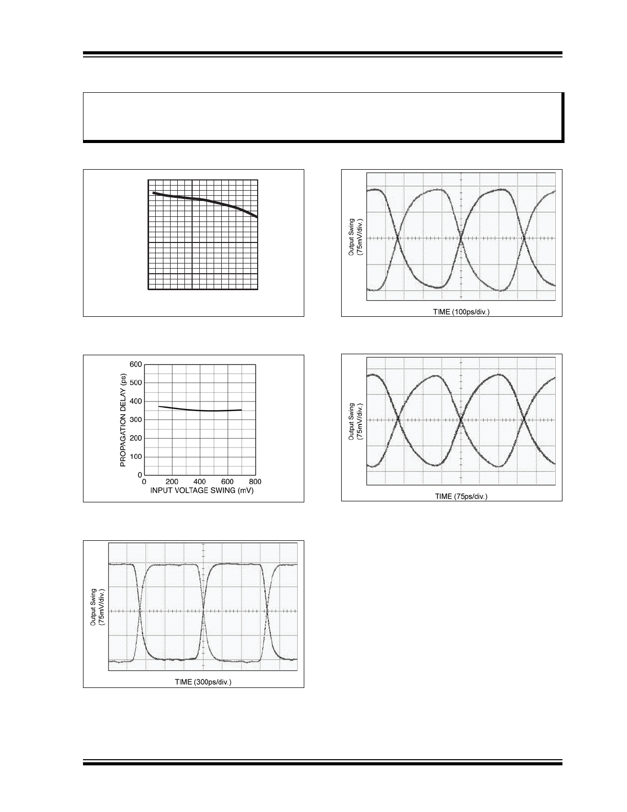
FIGURE 2-1:
Output Swing vs.
Frequency.
FIGURE 2-2:
Propagation Delay vs. Input
Voltage Swing.
FIGURE 2-3:
500 MHz Output.
FIGURE 2-4:
1.5 GHz Output.
FIGURE 2-5:
2 GHz Output.
Note:
The graphs and tables provided following this note are a statistical summary based on a limited number of
samples and are provided for informational purposes only. The performance characteristics listed herein
are not tested or guaranteed. In some graphs or tables, the data presented may be outside the specified
operating range (e.g., outside specified power supply range) and therefore outside the warranted range.
0
50
100
150
200
250
300
350
0
0.5
1
1.5
2
2.5
AMPLITUDE (mV)
FREQUENCY (GHz)
SY89833AL
DS20005608A-page 8
2018 Microchip Technology Inc.
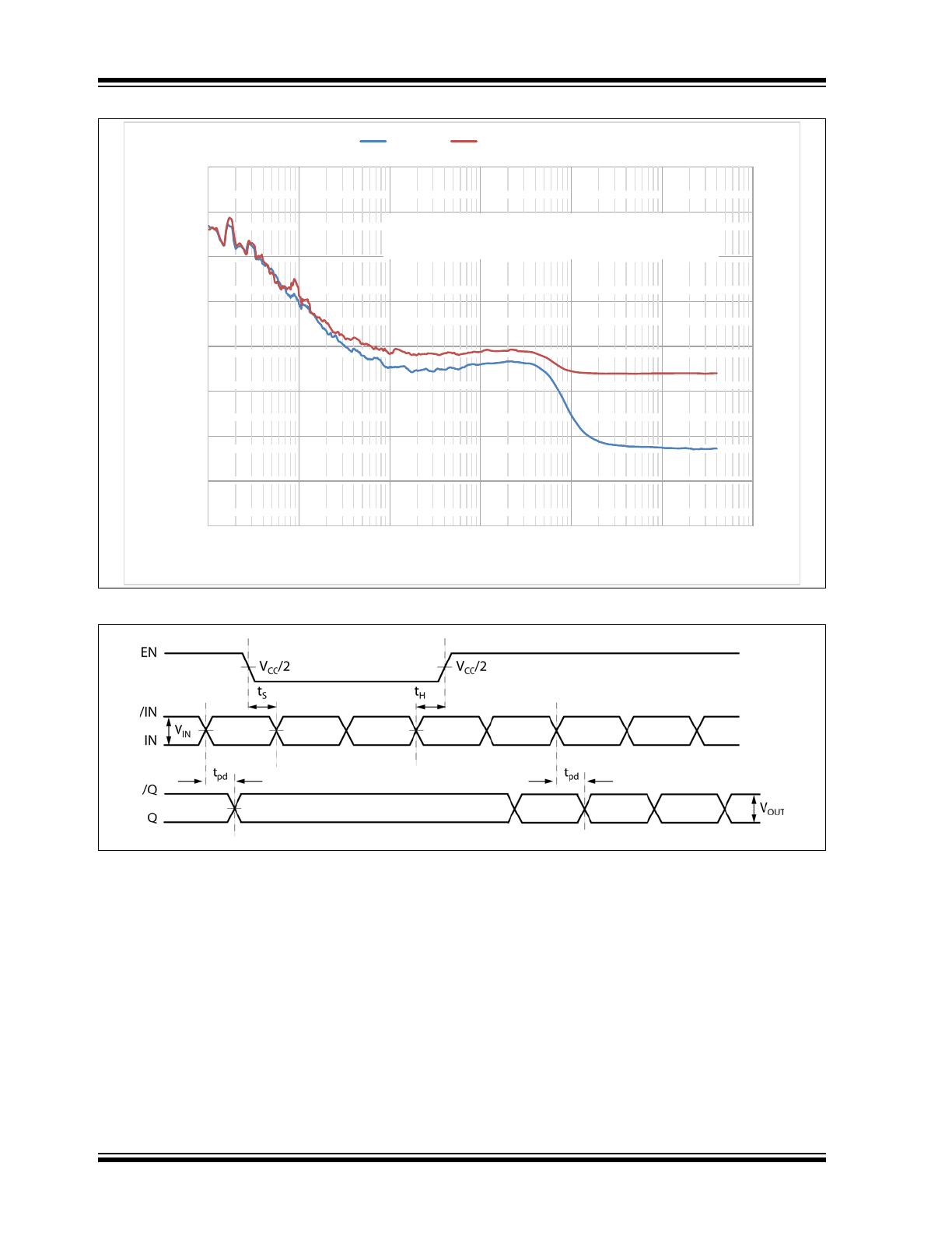
FIGURE 2-6:
Typical Additive Phase Jitter.
FIGURE 2-7:
Timing Diagram.
-180.00
-170.00
-160.00
-150.00
-140.00
-130.00
-120.00
-110.00
-100.00
0.0001
0.001
0.01
0.1
1
10
100
Ph
ase N
o
ise
(d
Bc/H
z)
Oīset Frequency (MHz)
REF input
SY89833AL output
TYPICAL ADDITIVE PHASE JITTER @622.08MHz, 3.3V
12kHz - 20MHz RANGE = 80fs
2018 Microchip Technology Inc.
DS20005608A-page 9
SY89833AL
3.0
PIN DESCRIPTIONS
The descriptions of the pins are listed in
Table 3-1
.
TABLE 3-1:
PIN FUNCTION TABLE
Pin Number
Pin Name
Description
15, 16
1, 2
3, 4
5, 6
Q0, /Q0
Q1, /Q1
Q2, /Q2
Q3, /Q3
LVDS Differential Outputs: Normally terminated with 100Ω across the pair (Q, /Q).
See the
LVDS Outputs
section,
Figure 5-1
. Unused outputs should be terminated with
a 100Ω resistor across each pair.
8
EN
This single-ended TTL/CMOS-compatible input functions as a synchronous output
enable. The synchronous enable ensures that enable/disable will only occur when the
outputs are in a logic low state. Note that this input is internally connected to a 25 kΩ
pull-up resistor and will default to logic high state (enabled) if left open.
9, 12
/IN, IN
Differential Input: This input pair is the differential signal input to the device. Input
accepts AC- or DC-Coupled differential signals as small as 100 mV. Each pin of the
pair internally terminates to a V
T
pin through 50Ω. Note that this input will default to an
intermediate state if left open. Please refer to the
Input Interface Applications
section
for more details.
10
V
REF-AC
Reference Voltage: These outputs bias to V
CC
– 1.425V.They are used when AC
coupling the inputs (IN, /IN). For AC-coupled applications, connect V
REF-AC
to V
T
pin
and bypass with 0.01 µF low-ESR capacitor to V
CC
. See the
Input Interface
Applications
section for more details. Maximum sink/source current is ±1.5 mA.
11
V
T
Input Termination Center-Tap: Each side of the differential input pair terminates to a
V
T
pin. The V
T
pin provides a center-tap to a termination network for maximum
interface flexibility. See the
Input Interface Applications
section for more details.
13
GND
Ground. GND pin and exposed pad must be connected to the most negative potential
of the device ground.
7, 14
V
CC
Positive Power Supply: Bypass with 0.1 µF//0.01 µF low-ESR capacitors and place as
close as possible to each V
CC
pin.
TABLE 3-2:
TRUTH TABLE
IN
/IN
EN
Q
/Q
0
1
1
0
1
1
0
1
1
0
X
X
0
0 (
Note 1
)
1 (
Note 1
)
Note 1:
On next negative transition of the input signal (IN).
SY89833AL
DS20005608A-page 10
2018 Microchip Technology Inc.
4.0
INPUT INFORMATION
4.1
Input Stage
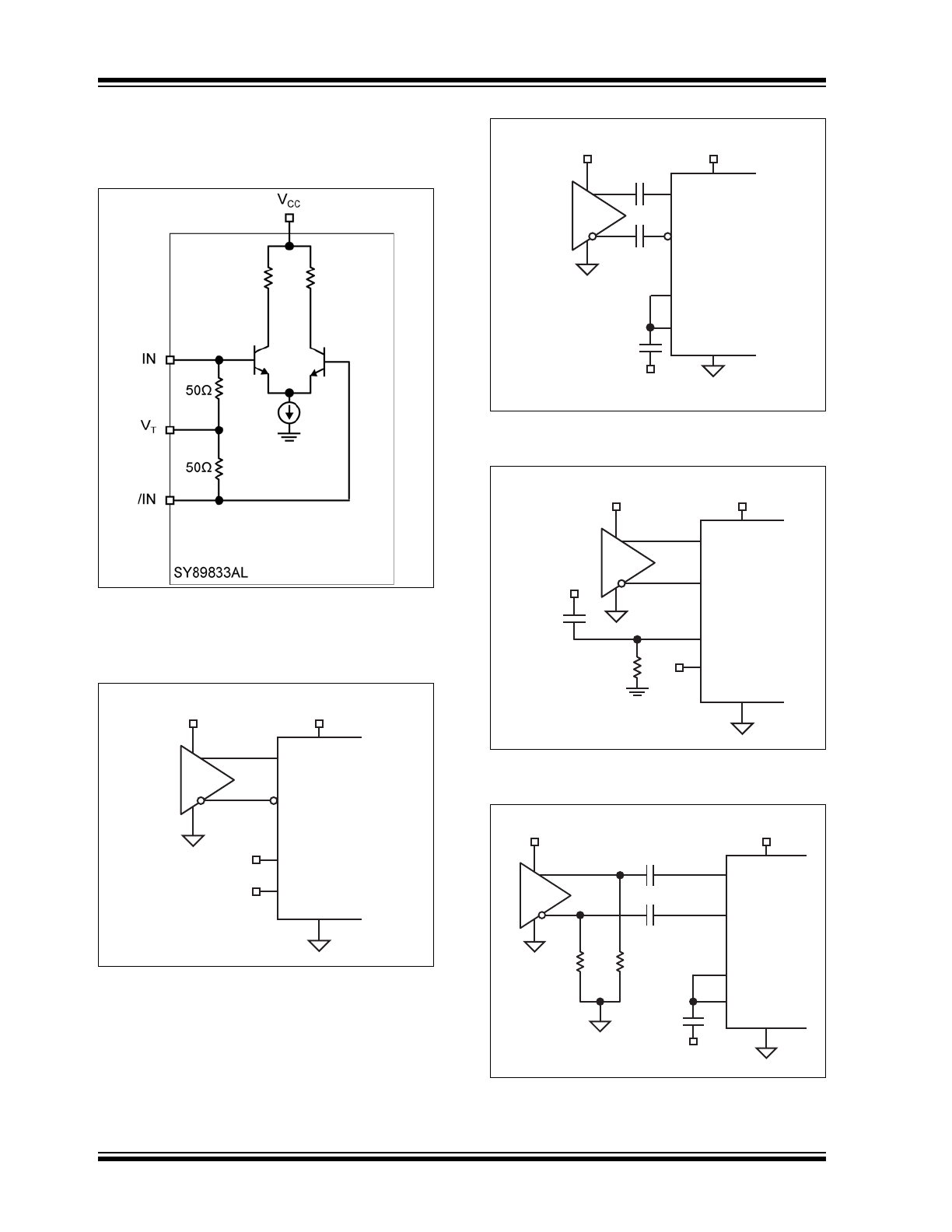
FIGURE 4-1:
Simplified Differential Input
Buffer.
4.2
Input Interface Applications
FIGURE 4-2:
DC-Coupled CML Input
Interface (Option: May Connect V
T
to V
CC
).
FIGURE 4-3:
AC-Coupled CML Input
Interface.
FIGURE 4-4:
DC-Coupled LVPECL Input
Interface.
FIGURE 4-5:
AC-Coupled LVPECL Input
Interface.
NC
CML
IN
/IN
VT
NC
SY89833AL
V
CC
= 3.3V
V
CC
= 3.3V
VREF-AC
CML
IN
/IN
VT
V
CC
= 3.3V
V
CC
= 3.3V
V
CC
SY89833AL
VREF-AC
0.01μF
LVPECL
IN
/IN
VT
V
CC
= 3.3V
V
CC
= 3.3V
SY89833AL
VREF-AC
V
CC
–2V
NC
50
0.01μF
V
CC
IN
/IN
VT
Rpd
100
Rpd
100
V
CC
= 3.3V
V
CC
= 3.3V
SY89833AL
VREF-AC
V
CC
0.01μF
LVPECL