
2018 Microchip Technology Inc.
DS20005931A-page 1
SY100ELT22L
Features
• 3.3V Power Supply
• 300 ps Typical Propagation Delay
• <100 ps Output-to-Output Skew
• Differential LVPECL Outputs
• PNP LVTTL Inputs for Minimal Loading
• Flow-Through Pinouts
• Available in 8-Lead SOIC Package
General Description
The SY100ELT22L is a dual LVTTL-to-differential
LVPECL translator with +3.3V power supply. Because
LVPECL levels are used, only +3.3V and ground are
required. The small-outline 8-lead SOIC package and
the low skew, dual gate design of the ELT22L make it
ideal for applications that require the translation of a
clock and a data signal.
The SY100ELT22L is compatible with positive ECL
100K logic levels.
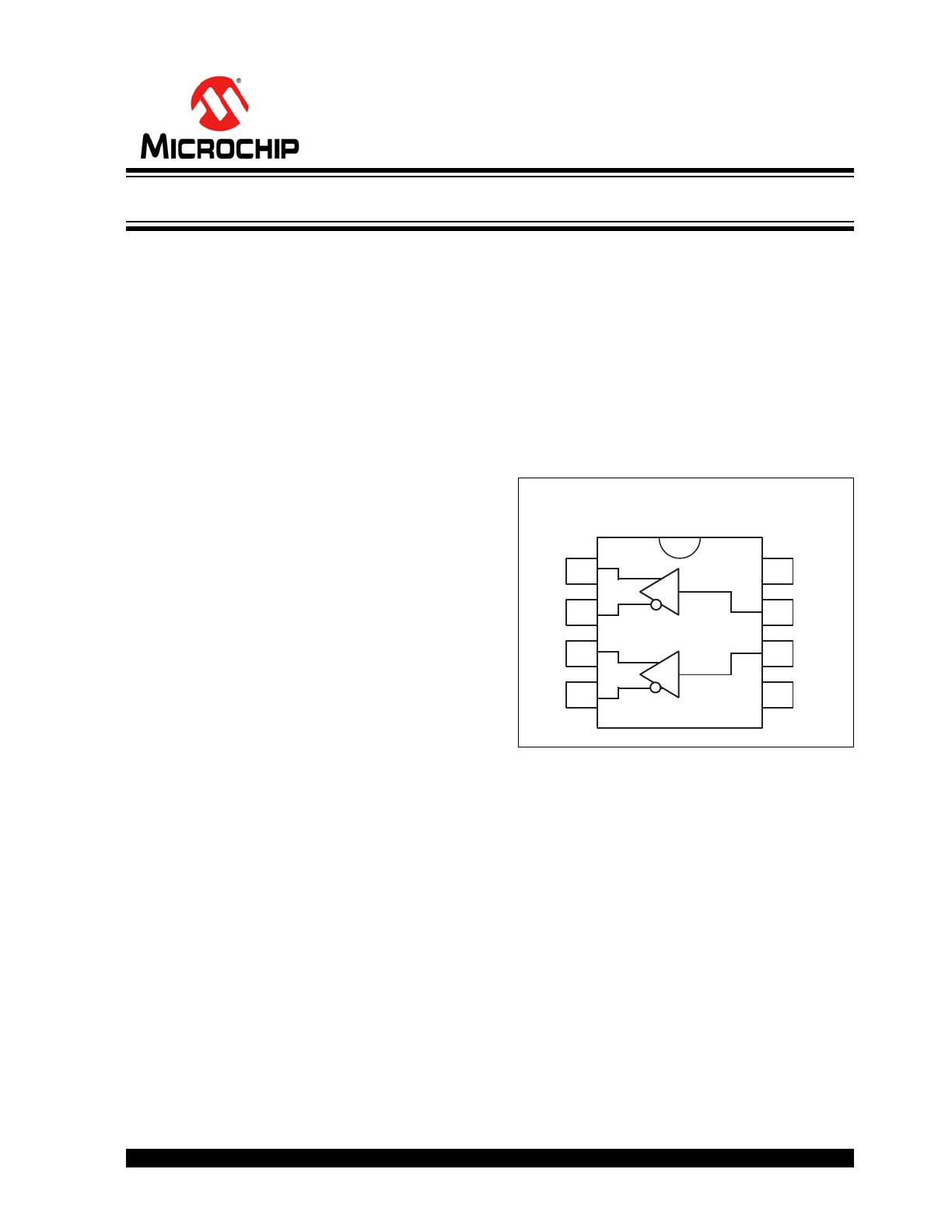
Package Type
SY100ELT22L
8-Lead SOIC (Z8-1)
1
Q0
/Q0
Q1
/Q1
8 VCC
D0
GND
7
6
5
2
3
4
D1
LVPECL
LVTTL
3.3V Dual LVTTL-to-Differential LVPECL Translator
SY100ELT22L
DS20005931A-page 2
2018 Microchip Technology Inc.
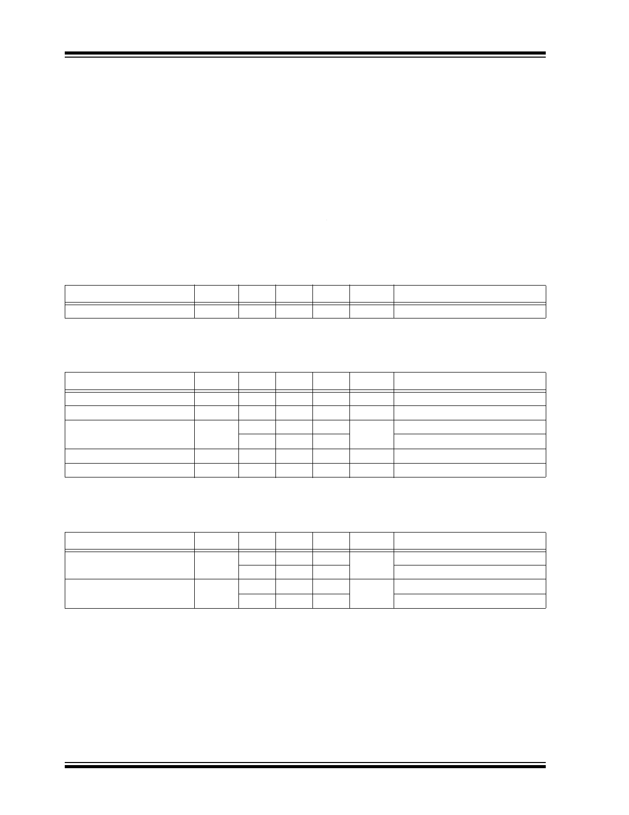
1.0
ELECTRICAL CHARACTERISTICS
Absolute Maximum Ratings †
Supply Voltage (V
CC
) ................................................................................................................................ –0.5V to +7.0V
LVTTL Input Voltage (V
IN
) ............................................................................................................................ –0.5V to V
CC
LVTTL Input Current (I
IN
).................................................................................................................... –30 mA to +5.0 mA
LVPECL Output Current (Continuous).....................................................................................................................50 mA
LVPECL Output Current (Surge) ...........................................................................................................................100 mA
†
Notice: Stresses above those listed under “Absolute Maximum Ratings” may cause permanent damage to the device.
This is a stress rating only and functional operation of the device at those or any other conditions above those indicated
in the operational sections of this specification is not intended. Exposure to maximum rating conditions for extended
periods may affect device reliability.
TABLE 1-1:
DC ELECTRICAL CHARACTERISTICS
Electrical Characteristics:
V
CC
= +3.0V to +3.8V, T
A
= –40°C to +85°C, unless noted.
Parameter
Symbol
Min.
Typ.
Max.
Units
Conditions
Power Supply Current
I
CC
—
—
25
mA
—
TABLE 1-2:
LVTTL DC ELECTRICAL CHARACTERISTICS
Electrical Characteristics:
V
CC
= +3.0V to +3.8V, T
A
= –40°C to +85°C unless noted.
Parameter
Symbol
Min.
Typ.
Max.
Units
Conditions
Input High Voltage
V
IH
2.0
—
—
V
—
Input Low Voltage
V
IL
—
—
0.8
V
—
Input High Current
I
IH
—
—
20
µA
V
IN
= 2.7V
—
—
100
V
IN
= V
CC
Input Low Current
I
IL
—
—
–0.2
mA
V
IN
= 0.5V
Input Clamp Voltage
V
IK
—
—
–1.2
V
I
IN
= –18 mA
TABLE 1-3:
LVPECL DC ELECTRICAL CHARACTERISTICS
Electrical Characteristics:
V
CC
= +3.0V to +3.8V.
Parameter
Symbol
Min.
Typ.
Max.
Units
Conditions
Output High Voltage
V
OH
2220
—
2420
mV
T
A
= –40°C,
Note 1
.
2275
—
2420
T
A
= 0°C to +85°C,
Note 1
.
Output Low Voltage
V
OL
1470
—
1750
mV
T
A
= –40°C,
Note 1
.
1490
—
1680
T
A
= 0°C to +85°C,
Note 1
.
Note 1:
Values are for V
CC
= 3.3V. Level specifications will vary 1:1 with V
CC
.
2018 Microchip Technology Inc.
DS20005931A-page 3
SY100ELT22L
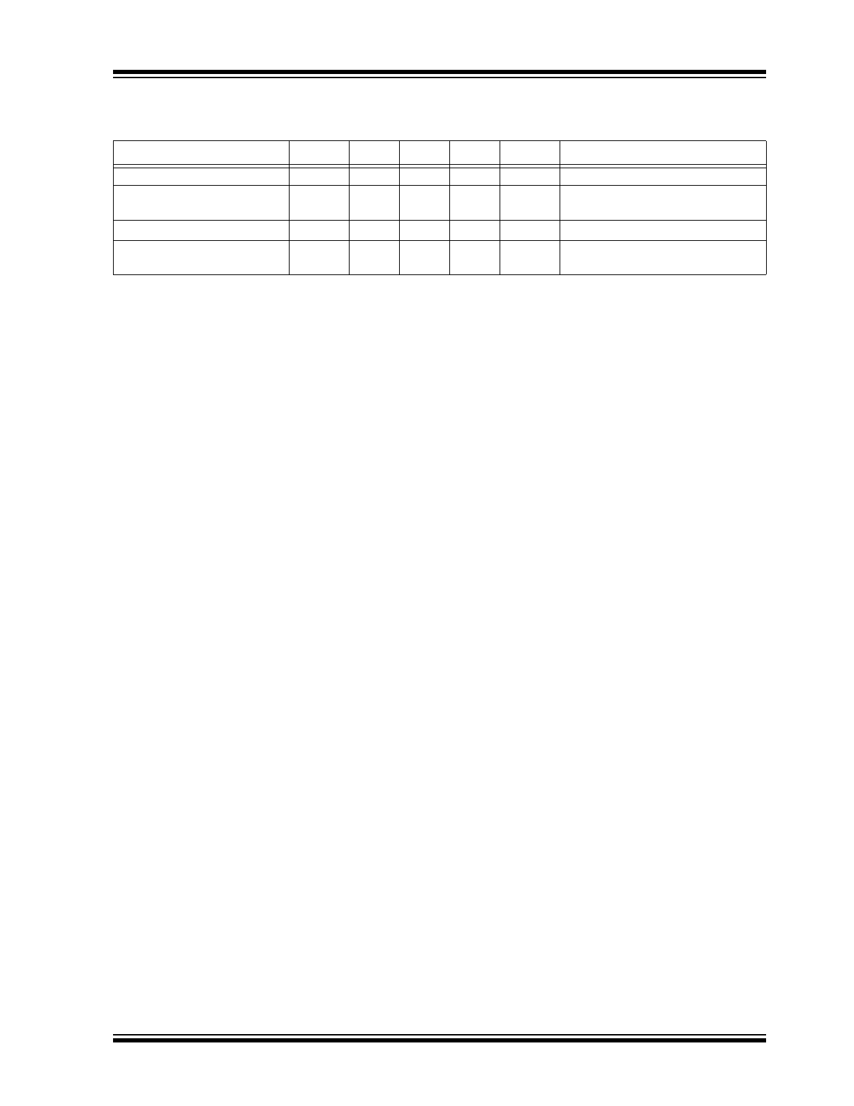
TABLE 1-4:
AC ELECTRICAL CHARACTERISTICS
Electrical Characteristics:
V
CC
= +3.0V to +3.8V; T
A
= –40°C to +85°C, unless otherwise stated.
Parameter
Symbol
Min.
Typ.
Max.
Units
Conditions
Propagation Delay to Output
t
PD
100
—
600
ps
50Ω to V
CC
– 2.0V
Output Rise/Fall Time, 20% to
80%
t
r
/t
f
200
—
500
ps
50Ω to V
CC
– 2.0V
Part-to-Part Skew,
Note 1
t
SKPP
—
—
500
ps
50Ω to V
CC
– 2.0V
Within-Device Skew,
Note 1
,
Note 2
t
SKEW
—
—
100
ps
50Ω to V
CC
– 2.0V
Note 1:
Guaranteed, but not tested.
2:
Same transition at common V
CC
levels.

SY100ELT22L
DS20005931A-page 4
2018 Microchip Technology Inc.
TEMPERATURE SPECIFICATIONS (
Note 1
)
Parameters
Sym.
Min.
Typ.
Max.
Units
Conditions
Temperature Ranges
Operating Temperature Range
T
A
–40
—
+85
°C
—
Storage Temperature Range
T
S
–65
—
+150
°C
—
Lead Temperature
—
—
—
+260
°C
Soldering, 20s
Note 1:
The maximum allowable power dissipation is a function of ambient temperature, the maximum allowable
junction temperature and the thermal resistance from junction to air (i.e., T
A
, T
J
,
JA
). Exceeding the
maximum allowable power dissipation will cause the device operating junction temperature to exceed the
maximum +85°C rating. Sustained junction temperatures above +125°C can impact the device reliability.
2018 Microchip Technology Inc.
DS20005931A-page 5
SY100ELT22L
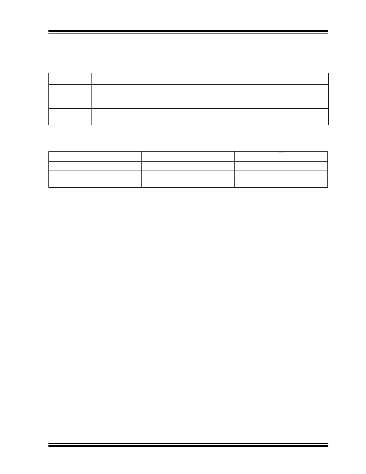
2.0
PIN DESCRIPTIONS
The descriptions of the pins are listed in
Table 2-1
.
2.1
Truth Table
TABLE 2-1:
PIN FUNCTION TABLE
Pin Number
Pin Name
Description
1, 2, 3, 4
Q0, /Q0
Q1, /Q1
Differential LVPECL Outputs.
5
GND
Ground.
6, 7
D1, D0
LVTTL Inputs
8
VCC
+3.3V Supply
TABLE 2-2:
TRUTH TABLE
D
Q
Q
H
H
L
L
L
H
Open
H
L
SY100ELT22L
DS20005931A-page 6
2018 Microchip Technology Inc.
3.0
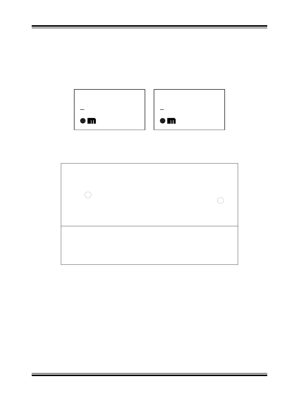
PACKAGING INFORMATION
3.1
Package Marking Information
Example
8-Lead SOIC*
WNNN
XXXXXX
4569
XEL22L
Legend:
XX...X
Product code or customer-specific information
Y
Year code (last digit of calendar year)
YY
Year code (last 2 digits of calendar year)
WW
Week code (week of January 1 is week ‘01’)
NNN
Alphanumeric traceability code
Pb-free JEDEC
®
designator for Matte Tin (Sn)
*
This package is Pb-free. The Pb-free JEDEC designator ( )
can be found on the outer packaging for this package.
●, ▲, ▼ Pin one index is identified by a dot, delta up, or delta down (triangle
mark).
Note
:
In the event the full Microchip part number cannot be marked on one line, it will
be carried over to the next line, thus limiting the number of available
characters for customer-specific information. Package may or may not include
the corporate logo.
Underbar (_) and/or Overbar (⎯) symbol may not be to scale.
3
e
3
e
2018 Microchip Technology Inc.
DS20005931A-page 7
SY100ELT22L
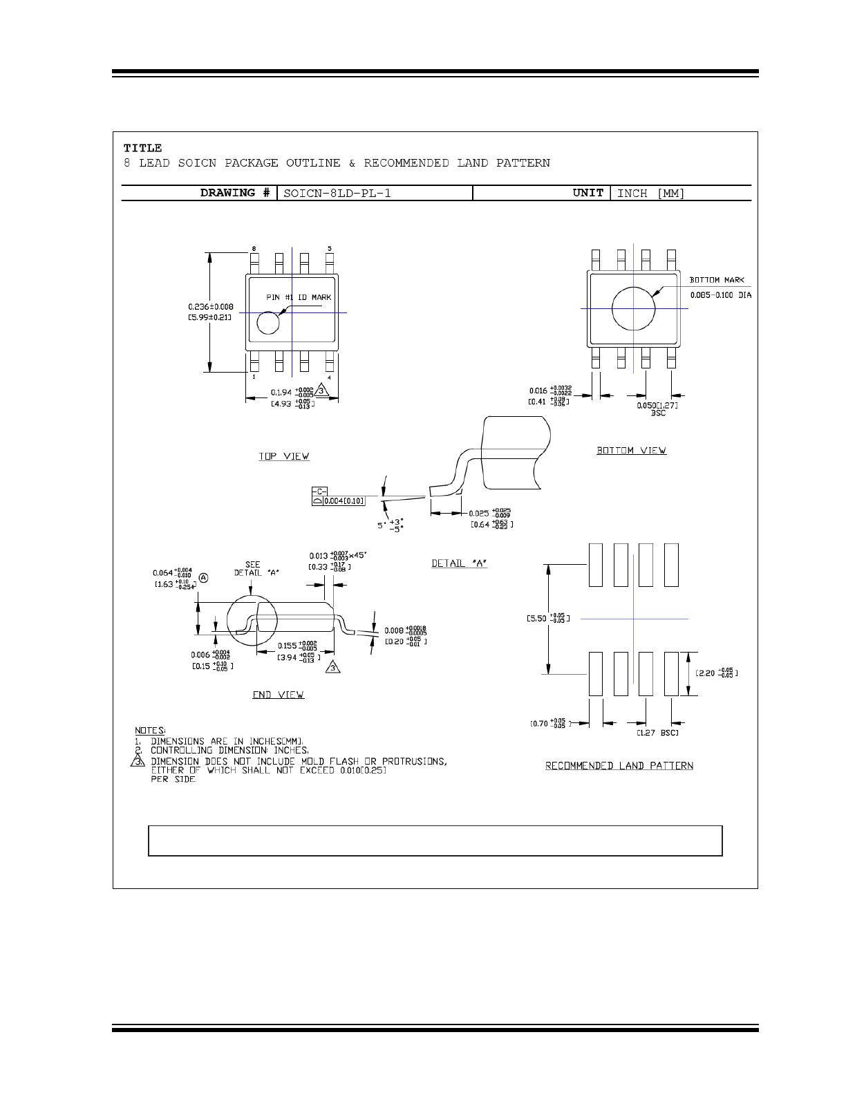
8-Lead SOIC Package Outline and Recommended Land Pattern
Note: For the most current package drawings, please see the Microchip Packaging Specification located at
http://www.microchip.com/packaging.

SY100ELT22L
DS20005931A-page 8
2018 Microchip Technology Inc.
NOTES:

2018 Microchip Technology Inc.
DS20005931A-page 9
SY100ELT22L
APPENDIX A:
REVISION HISTORY
Revision A (January 2018)
• Converted Micrel document SY100ELT22L to
Microchip data sheet DS20005931A.
• Minor text changes throughout.

SY100ELT22L
DS20005931A-page 10
2018 Microchip Technology Inc.
NOTES: