
© 2008 Microchip Technology Inc.
DS21394D-page 1
TC14433/A
Features:
• Accuracy: ±0.05% of Reading ±1 Count
• Two Voltage Ranges: 1.999V and 199.9 mV
• Up to 25 Conversions Per Second
• Z
IN
> 1000M Ohms
• Single Positive Voltage Reference
• Auto-Polarity and Auto-Zero
• Overrange and Underrange Signals Available
• Operates in Auto-Ranging Circuits
• Uses On-Chip System Clock or External Clock
• Wide Supply Range: ±4.5V to ±8V
Applications:
• Portable Instruments
• Digital Voltmeters
• Digital Panel Meters
• Digital Scales
• Digital Thermometers
• Remote A/D Sensing Systems
Description
The TC14433 is a low-power, high-performance,
monolithic CMOS 3-1/2 digit A/D converter. The
TC14433 combines both analog and digital circuits on
a single IC, thus minimizing the number of external
components.
This dual slope A/D converter provides automatic
polarity and zero correction with the addition of two
external resistors and two capacitors. The full scale
voltage range of this ratiometric IC extends from
199.9 millivolts to 1.999 volts. The TC14433 can
operate over a wide range of power supply voltages,
including batteries and standard 5-volt supplies.
The TC14433A features improved performance over
the industry standard TC14433. Rollover, which is the
measurement of identical positive and negative
signals, is specified to have the same reading within
one count for the TC14433A. Power consumption of
the TC14433A is typically 4 mW, approximately one-
half that of the industry standard TC14433.
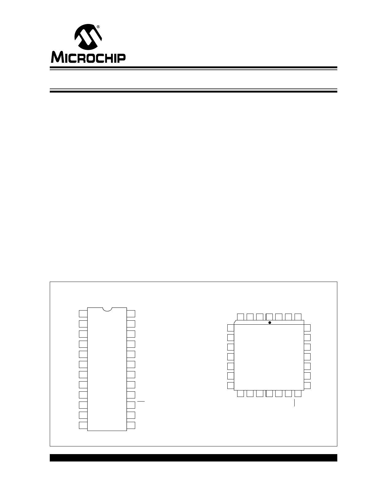
The TC14433/A is available in 24-Pin PDIP, 24-Pin
SOIC (TC14433 device only), and 28-Pin PLCC
packages.
Package Type
Note 1:
NC = No internal connection (In 28-Pin PLCC).
2:
24-Pin SOIC (Wide) package, only for TC14433
device.
1
2
3
4
16
15
14
5
6
7
8
13
19
18
17
9
10
11
12
20
21
22
23
24 V
DD
Q
3
Q
2
Q
1
Q
0
DS
1
DS
3
DS
2
DS
4
EOC
OR
R
1
C
1
CO
1
CO
2
R
1
/C
1
CLK0
CLK1
DU
V
EE
V
SS
V
AG
V
X
V
REF
TC14433/A
24-Pin PDIP (Wide)
24-Pin SOIC (Wide)
V
REF
NC
V
DD
Q
3
Q
1
Q
0
DS
2
DS
3
DS
1
DS
4
Q
2
V
AG
V
X
CO
1
V
EE
CO
2
R
1
/C
1
C
1
R
1
V
SS
EOC
NC
NC
NC
DU
CLK0
CLK1
19
20
21
22
23
24
25
11
10
9
8
7
6
5
TC14433/A
12 13 14 15
17 18
4
3
2
1
27 26
28
16
28-Pin PLCC
OR
3-1/2 Digit, Analog-to-Digital Converter
TC14433/A
DS21394D-page 2
© 2008 Microchip Technology Inc.
Typical Application
3
1
4
5
6
7
8
23
22
21
20
13
9
14
15 19 18 17 16
11 10 2 12 24
4
2
3
5
9
10
11
12
13
14
15
1
7
6
5
4
3
2
1
10
11
12
13
14
15
16
R
1
*
V
X
20 k
Ω
D
C
S
R
TC14433
Q
Q
D
C
S
R
+5V
-5V
16
+5V
+5V
Segment
Resistors
150
Ω (7)
+5V
Q
Q
-5V
-5V
-5V
-5V
8
Minus Sign
200
Ω
51 k
Ω
6 7
+5V
-5V
-5V
-5V
MPS-A12
(4)
Common
Anode Led
Display
MPS-A12
300
R
C
14013B
5
3
9
11
1
2
13
12
6
7
14
10
f g e d c b a
+5V
1 µF
4
8
DS4
DS3
DS2
DS1
-5V
MCP1525
4543B
1413
V
IN
V
OUT
V
SS
Plus Sign
110
Ω
1 µF
0.1 µF**
0.1 µF**
k
Ω
0.1 µF
0.1 µF
0.1 µF
50 µF
*R
1
= 470 k
Ω for 2V Range
*
R
1
= 27 k
Ω for 200 mV Range
**Mylar Capacitor
© 2008 Microchip Technology Inc.
DS21394D-page 3
TC14433/A
1.0
ELECTRICAL
CHARACTERISTICS
Absolute Maximum Ratings†
Supply Voltage (V
DD
– V
EE
) ................... -0.5V to +18V
Voltage on Any Pin:
Reference to V
EE
.....................-0.5V to (V
DD
+ 0.5)
DC Current, Any Pin: ....................................... ±10 mA
Power Dissipation (T
A
≤ 70°C):
Plastic PLCC ................................................. 1.0W
Plastic PDIP.............................................. 940 mW
SOIC ......................................................... 940 mW
Operating Temperature Range ............ -40°C to +85°C
Storage Temperature Range .............. -65°C to +160°C
† Notice: Stresses above those listed under “Absolute
Maximum Ratings” may cause permanent damage to
the device. These are stress ratings only and functional
operation of the device at these or any other conditions
above those indicated in the operation sections of the
specifications is not implied. Exposure to Absolute
Maximum Rating conditions for extended periods may
affect device reliability.
TC14433/A ELECTRICAL SPECIFICATIONS
Electrical Characteristics: Unless otherwise specified, V
DD
= +5V, V
EE
= -5V, C
1
= 0.1 µF, (Mylar), C
0
= 0.1 µF,
R
C
= 300 k
Ω, R
1
= 470 k
Ω @ V
REF
= 2V, R
1
= 27 k
Ω @ V
REF
= 200 mV, T
A
= +25°C.
Parameter
Symbol
Min
Typ
Max
Min
Typ
Max
Units
Test Conditions
Analog Input
Rollover Error (Positive) and
Negative Full Scale
Symmetry
SYE
-1
—
+1
—
—
—
Counts
200 mV Full Scale
V
IN
-V
IN
= +V
IN
Linearity Output Reading
(Note 1)
NL
-0.05
+0.05
+0.05
—
—
—
%rdg
V
REF
= 2V
-1 count
—
+1 count
—
—
—
%rdg
V
REF
= 200 mV
Stability Output Reading
(Note 2)
SOR
—
—
2
—
—
—
LSD
V
X
= 1.99V,
V
REF
= 2V
—
—
3
—
—
—
LSD
V
X
= 199 mV,
V
REF
= 200 mV
Zero Output Reading
ZOR
—
0
0
—
—
—
LSD
V
X
= 0V, V
REF
= 2V
Bias Current: Analog Input
Reference Input
Analog Ground
I
IN
—
±20
±100
—
—
—
pA
—
±20
±100
—
—
—
pA
—
±20
±100
—
—
—
pA
Common mode Rejection
CMRR
—
65
—
—
—
—
dB
V
X
= 1.4V, V
REF
= 2V,
F
OC
= 32 kHz
Note
1:
Accuracy – The accuracy of the meter at full scale is the accuracy of the setting of the reference voltage. Zero is
recalculated during each conversion cycle. The meaningful specification is linearity. In other words, the deviation from
correct reading for all inputs other than positive full scale and zero is defined as the linearity specification.
2:
The LSD stability for 200 mV scale is defined as the range that the LSD will occupy 95% of the time.
3:
Pin numbers refer to 24-pin PDIP.
TC14433/A
DS21394D-page 4
© 2008 Microchip Technology Inc.
TEMPERATURE SPECIFICATIONS
Digital
Output Voltage
(Pins 14 to 23) (Note 3)
V
OL
—
0
0.05
—
—
0.05
V
V
SS
= 0V, “0” Level
—
-5
-4.95
—
—
-4.95
V
V
SS
= -5V, “0” Level
Output Voltage
(Pins 14 to 23) (Note 3)
V
OH
4.95
5
—
4.95
—
—
V
V
SS
= 0V, “1” Level
4.95
5
—
4.95
—
—
V
V
SS
= -5V, “1” Level
Output Current
(Pins 14 to 23)
I
OH
-0.2
-0.36
—
-0.14
—
—
mA
V
SS
= 0V, V
OH
= 4.6V
Source
- 0.5
-0.9
—
-0.35
—
—
mA
V
SS
= -5V, V
OH
= 5V
Source
Output Current
(Pins 14 to 23)
I
OL
0.51
0.88
—
0.36
—
—
mA
V
SS
= 0V, V
OL
= 0.4V
Sink
1.3
2.25
—
0.9
—
—
mA
V
SS
= -5V,
V
OL
= -4.5V Sink
Clock Frequency
f
CLK
—
66
—
—
—
—
kHz
R
C
= 300 k
Ω
Input Current -DU
I
DU
—
±0.00
001
±0.3
—
—
±1
µA
Power
Quiescent Current:
TC14433A:
I
Q
—
—
—
—
—
—
—
V
DD
to V
EE
, I
SS
= 0
—
0.4
2
—
—
3.7
mA
V
DD
= 5, V
EE
= -5
—
1.4
4
—
—
7.4
mA
V
DD
= 8, V
EE
= -8
Quiescent Current:
TC14433
—
—
—
—
—
—
—
V
DD
to V
EE
, I
SS
= 0
—
0.9
2
—
—
3.7
mA
V
DD
= 5, V
EE
= -5
—
1.8
4
—
—
7.4
mA
V
DD
= 8, V
EE
= -8
Supply Rejection
PSRR
—
0.5
—
—
—
—
mV/V
V
DD
to V
EE
, I
SS
= 0,
V
REF
= 2V,
V
DD
= 5, V
EE
= -5
TC14433/A ELECTRICAL SPECIFICATIONS (CONTINUED)
Electrical Characteristics: Unless otherwise specified, V
DD
= +5V, V
EE
= -5V, C
1
= 0.1 µF, (Mylar), C
0
= 0.1 µF,
R
C
= 300 k
Ω, R
1
= 470 k
Ω @ V
REF
= 2V, R
1
= 27 k
Ω @ V
REF
= 200 mV, T
A
= +25°C.
Parameter
Symbol
Min
Typ
Max
Min
Typ
Max
Units
Test Conditions
Note
1:
Accuracy – The accuracy of the meter at full scale is the accuracy of the setting of the reference voltage. Zero is
recalculated during each conversion cycle. The meaningful specification is linearity. In other words, the deviation from
correct reading for all inputs other than positive full scale and zero is defined as the linearity specification.
2:
The LSD stability for 200 mV scale is defined as the range that the LSD will occupy 95% of the time.
3:
Pin numbers refer to 24-pin PDIP.
Electrical Characteristics: Unless otherwise indicated, V
DD
= +5V and V
EE
= -5V.
Parameters
Sym
Min
Typ
Max
Units
Conditions
Temperature Ranges
Operating Temperature Range
T
A
-40
—
+85
°C
Note
Storage Temperature Range
T
A
-65
—
+150
°C
Thermal Package Resistances
Thermal Resistance, 24LD PDIP
θ
JA
—
60.5
—
°C/W
Thermal Resistance, 24LD CERDIP
θ
JA
—
N/A
—
°C/W
Thermal Resistance,24LD SOIC Wide
θ
JA
—
70
—
°C/W
Thermal Resistance, 28LD PLCC
θ
JA
—
61.2
—
°C/W
Note:
The internal junction temperature (T
J
) must not exceed the absolute maximum specification of +150°C.
© 2008 Microchip Technology Inc.
DS21394D-page 5
TC14433/A
2.0
TYPICAL PERFORMANCE CURVES
Note:
Unless otherwise specified, V
DD
= +5V, V
EE
= -5V, C
1
= 0.1 µF, (Mylar), C
0
= 0.1 µF, R
C
= 300 k
Ω, R
1
= 470 k
Ω @ V
REF
= 2V,
R
1
= 27 k
Ω @ V
REF
= 200 mV, T
A
= +25°C.
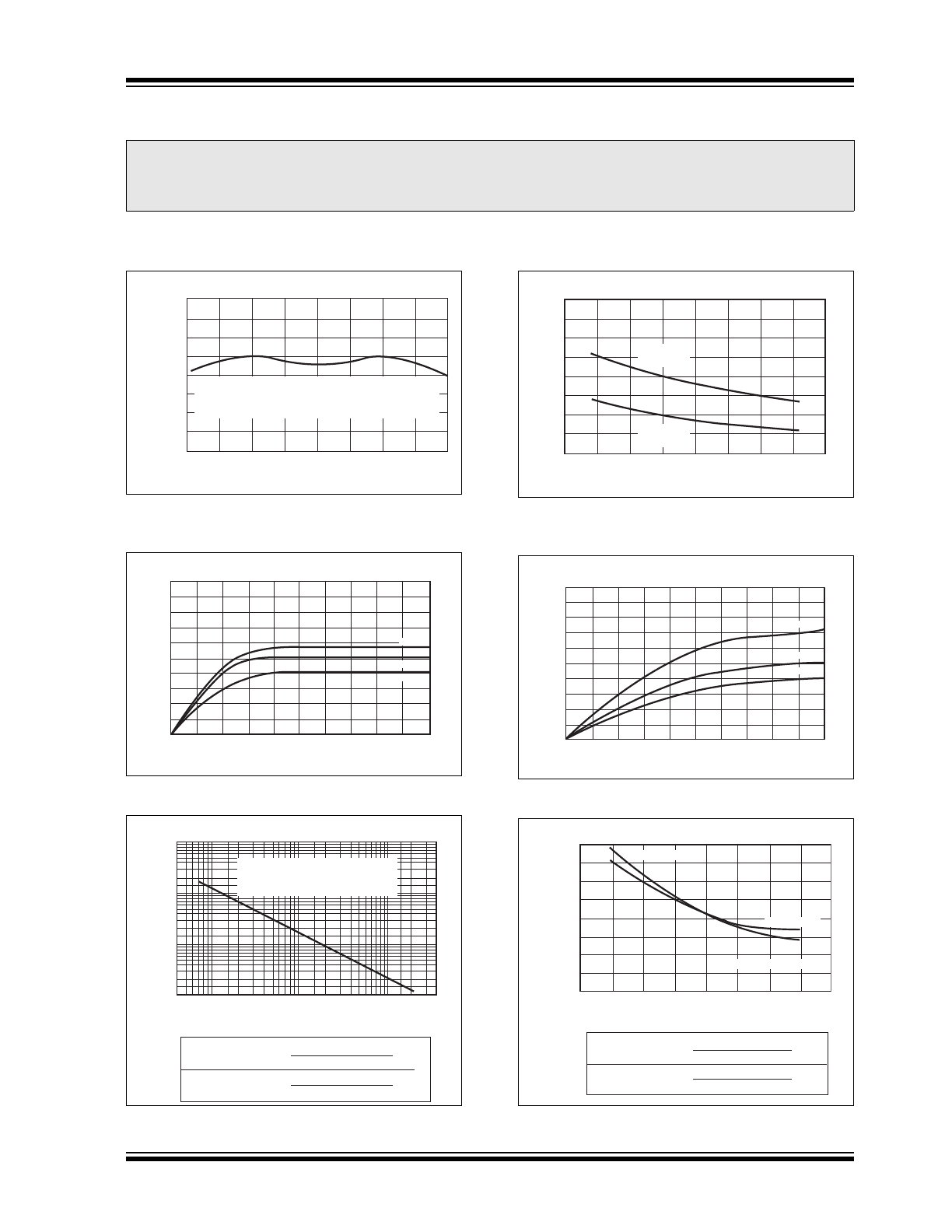
FIGURE 2-1:
Rollover Error vs. Power
Supply Skew
FIGURE 2-2:
Sink Current at V
DD
= 5V.
FIGURE 2-3:
Clock Frequency vs.
Resistor (R
C
)
FIGURE 2-4:
Quiescent Power Supply
Current vs. Ambient Temperature.
FIGURE 2-5:
Sink Current at VDD = 5V.
FIGURE 2-6:
% Change to Clock
Frequency vs. Ambient Temperature.
Note:
The graphs and tables provided following this note are a statistical summary based on a limited number of
samples and are provided for informational purposes only. The performance characteristics listed herein
are not tested or guaranteed. In some graphs or tables, the data presented may be outside the specified
operating range (e.g., outside specified power supply range) and therefore outside the warranted range.
ROLLOVER ERROR (IN LSD)
AT FULL SCALE
(PLUSE COUNT LESS MINUS COUNT)
-3
-2
-1
0
1
-4
-3
-2
-1
Typical Rollover Error vs. Power Supply Skew
(V
DD
I-IV
EE
I) - SUPPLY VOLTAGE SKEW (V)
0
1
2
3
4
2
3
4
Note: Rollover Error is the Difference in Output
Reading for the same Analog Input Switched
from Positive to Negative.
0
1
2
3
4
5
0
1
2
3
4
5
-40
°
C
+25
°
C
+85
°
C
Typical N-Channel Sink Current at V
DD
– V
SS
= 5 Volts
I
D
- SINK CURRENT (mA)
V
DS
- DRAIN TO SOURCE VOLTAGE (V
DC
)
1M
10k
10k
Ω
100k
Ω
1M
Ω
100k
CLOCK FREQUENCY
16,400
±1.5%
CONVERSION RATE =
Typical Clock Frequency vs. Resistor (R
C
)
I
CLK
- CLOCK FREQUENCY (Hz)
R
C
- CLOCK FREQUENCY RESISTOR
Note: ±5% Typical Variation over
Supply Voltage Range
of ±4.5V to ±8V
CLOCK FREQUENCY
80
MULTIPLEX RATE =
Typical Quiescent Power Supply Current vs.Temp.
I
Q
- QUIESCENT CURRENT (mA)
T
A
- TEMPERATURE (
°
C)
0
1
2
3
4
-40
-20
0
20
40
60
80
100
V
EE
= -8V
V
DD
= +8V
V
EE
= -5V
V
DD
= +5V
0
-1
-2
-3
0
-1
-2
-3
-4
-5
Typical P-Channel Sink Current at V
DD
– V
SS
= 5 Volts
I
D
- SINK CURRENT (mA)
V
DS
- DRAIN TO SOURCE VOLTAGE (V
DC
)
-40
°
C
+25
°
C
+85
°
C
4
3
2
1
0
-1
-2
-3
-4
-40
-20
0
20
40
60
80
Normalized at 25
°
C
±5V Supply
±8V Supply
I
CLK
- CLOCK FREQUENCY
(% CHANGE)
Typical % Change fo Clock Frequency vs. Temp.
CLOCK FREQUENCY
16,400
±1.5%
CONVERSION RATE =
CLOCK FREQUENCY
80
MULTIPLEX RATE =
T
A
- TEMPERATURE (
°
C)
TC14433/A
DS21394D-page 6
© 2008 Microchip Technology Inc.
3.0
PIN DESCRIPTIONS
The descriptions of the pins are listed in
Table 3-1
.
TABLE 3-1:
PIN FUNCTION TABLE
Pin No.
24-Pin PDIP,
SOIC
Pin No.
28-Pin
PLCC
Symbol
Description
1
2
V
AG
This is the analog ground. It has a high input impedance. The pin determines
the reference level for the unknown input voltage (V
X
) and the reference
voltage (V
REF
).
2
3
V
REF
Reference voltage – Full scale output is equal to the voltage applied to V
REF
.
Therefore, full scale voltage of 1.999V requires 2V reference and 199.9 mV
full scale requires a 200 mV reference. V
REF
functions as system reset also.
When switched to V
EE
, the system is reset to the beginning of the
conversion cycle.
3
4
V
X
The unknown input voltage (V
X
) is measured as a ratio of the reference
voltage (V
REF
) in a ratiometric A/D conversion.
4
5
R
1
This pin is for external components used for the integration function in the
dual slope conversion. Typical values are 0.1 µF (Mylar) capacitor for C
1
.
5
6
R
1
/C
1
R
1
= 470 k
Ω (resistor) for 2V full scale.
6
7
C
1
R
1
= 27 k
Ω (resistor) for 200 mV full scale. Clock frequency of 66 kHz gives
250 ms conversion time.
7
9
CO
1
These pins are used for connecting the offset correction capacitor. The
recommended value is 0.1 µF.
8
10
CO
2
These pins are used for connecting the offset correction capacitor. The
recommended value is 0.1 µF.
9
11
DU
Display update input pin. When DU is connected to the EOC output, every
conversion is displayed. New data will be strobed into the output latches
during the conversion cycle if a positive edge is received on DU, prior to the
ramp down cycle. When this pin is driven from an external source, the
voltage should be referenced to V
SS
.
10
12
CLK
1
Clock input pins. The TC14433 has its own oscillator system clock.
Connecting a single resistor between CLK
1
and CLK
0
sets the clock
frequency.
11
13
CLK
0
A crystal or OC circuit may be inserted in lieu of a resistor for improved
CLK
1
, the clock input, can be driven from an external clock source, which
need only have standard CMOS output drive. This pin is referenced to V
EE
for external clock inputs. A 300 k
Ω resistor yields a clock frequency of about
66 kHz. See Section 2.0 “Typical Performance Curves”. (Also see
Figure 5-3
for alternate circuits.)
12
14
V
EE
Negative power current. Connection pin for the most negative supply. Please
note the current for the output drive circuit is returned through V
SS
. Typical
supply current is 0.8 mA.
13
16
V
SS
Negative power supply for output circuitry. This pin sets the low voltage level
for the output pins (BCD, Digit Selects, EOC, OR). When connected to
analog ground, the output voltage is from analog ground to V
DD
. If
connected to V
EE
, the output swing is from V
EE
to V
DD
. The recommended
operating range for V
SS
is between the V
DD
-3 volts and V
EE
.
14
17
EOC
End of conversion output generates a pulse at the end of each conversion
cycle. This generated pulse width is equal to one half the period of the
system clock.
15
18
OR
Overrange pin. Normally this pin is set high. When V
X
exceeds V
REF
the OR
is low.
© 2008 Microchip Technology Inc.
DS21394D-page 7
TC14433/A
16
19
DS
4
Digit select pin. The digit select output goes high when the respective digit is
selected. The MSD (1/2 digit turns on immediately after an EOC pulse).
17
20
DS
3
The remaining digits turn on in sequence from MSD to LSD.
18
21
DS
2
To ensure that the BCD data has settled, an inter digit blanking time of two
clock periods is included.
19
23
DS
1
Clock frequency divided by 80 equals multiplex rate. For example, a system
clock of 60 kHz gives a multiplex rate of 0.8 kHz.
20
24
Q
0
See
Figure 5-4
for digit select timing diagram.
21
25
Q
1
BCD data output pin. Multiplexed BCD outputs contain three full digits of
information during digit select DS
2
, DS
3
, DS
4
.
22
26
Q
2
During DS
1
, the 1/2 digit, overrange, underrange and polarity information is
available.
23
27
Q
3
Refer to the Truth
Table 5-1
.
24
28
V
DD
Positive power supply. This is the most positive power supply pin.
—
1
NC
Not Used.
—
8
NC
Not Used.
—
15
NC
Not Used.
—
22
NC
Not Used.
TABLE 3-1:
PIN FUNCTION TABLE (CONTINUED)
Pin No.
24-Pin PDIP,
SOIC
Pin No.
28-Pin
PLCC
Symbol
Description
TC14433/A
DS21394D-page 8
© 2008 Microchip Technology Inc.
4.0
DETAILED DESCRIPTION
The TC14433 CMOS IC becomes a modified dual-
slope A/D with a minimum of external components.
This IC has the customary CMOS digital logic circuitry,
as well as CMOS analog circuitry. It provides the user
with digital functions such as (counters, latches,
multiplexers), and analog functions such as
(operational amplifiers and comparators) on a single
chip. Refer to the Functional Block diagram,
Figure 4-3
.
Features of the TC14433/A include auto-zero, high
input impedances and auto-polarity. Low power
consumption and a wide range of power supply
voltages are also advantages of this CMOS device.
The system’s auto-zero function compensates for the
offset voltage of the internal amplifiers and compara-
tors. In this “ratiometric system,” the output reading is
the ratio of the unknown voltage to the reference
voltage, where a ratio of 1 is equal to the maximum
count of 1999. It takes approximately 16,000 clock
periods to complete one conversion cycle. Each
conversion cycle may be divided into 6 segments.
Figure 4-1
shows the conversion cycle in 6 segments
for both positive and negative inputs.
i
FIGURE 4-1:
Integrator Waveforms at
Pin 6.
Segment 1 – The offset capacitor (C
O
), which compen-
sates for the input offset voltages of the buffer and
integrator amplifiers, is charged during this period.
However, the integrator capacitor is shorted. This
segment requires 4000 clock periods.
Segment 2 – During this segment, the integrator output
decreases to the comparator threshold voltage. At this
time, a number of counts equivalent to the input offset
voltage of the comparator is stored in the offset latches
for later use in the auto-zero process. The time for this
segment is variable and less than 800 clock periods.
Segment 3 – This segment of the conversion cycle is
the same as Segment 1.
Segment 4 – Segment 4 is an up going ramp cycle with
the unknown input voltage (V
X
as the input to the
integrator.
Figure 4-2
shows the equivalent
configuration of the analog section of the TC14433.
The actual configuration of the analog section is
dependent upon the polarity of the input voltage during
the previous conversion cycle.
FIGURE 4-2:
Equivalent Circuit Diagrams
of the Analog Section During Segment 4 of the
Timing Cycle
Segment 5 – This segment is a down-going ramp
period with the reference voltage as the input to the
integrator. Segment 5 of the conversion cycle has a
time equal to the number of counts stored in the offset
storage latches during Segment 2. As a result, the
system zeros automatically.
Segment 6 – This is an extension of Segment 5. The
time period for this portion is 4000 clock periods. The
results of the A/D conversion cycle are determined in
this portion of the conversion cycle.
Start
1
2
3
4
5
6
Typical
Positive
Input Voltage
Typical
Negative
Input Voltage
Time
Segment
Number
End
V
X
V
X
C
1
Comparator
R
1
Buffer
Integrator
+
–
+
–
+
–
V
X
© 2008 Microchip Technology Inc.
DS21394D-page 9
TC14433/A
FIGURE 4-3:
Functional Block Diagram.
Latches
1s'
10s'
100s'
1,000s'
Clock
RC
Control Logic
CMOS
Analog Subsystem
Display
Update
9
DU
End of
Conversion
EOC
14
R1
R1/C
C1
4
5
6
CO1 CO2
7
8
2
1
3
VREF
VAG
VX
Reference Voltage
Analog Ground
Analog Input
Offset
Polarity Detect
10
CLK 1
11
CLK 0
OR Overrange
Multiplexer
TC14433/A
20-23
16 -19
DS 1 – DS 4
Digit Strobe
Q – Q3
BDC Data
Integrator
15
Overflow
VDD = Pin 24
VSS = Pin 13
VEE = Pin 12
TC14433/A
DS21394D-page 10
© 2008 Microchip Technology Inc.
5.0
TYPICAL APPLICATIONS
The typical application circuit is an example of a 3-1/2
digit voltmeter using the TC14433 with Common-
anode displays. This system requires a 2.5V reference.
Full scale may be adjusted to 1.999V or 199.9 mV.
Input overrange is indicated by flashing a display. This
display uses LEDs with common anode digit lines.
Power supply for this system is shown as a dual ±5V
supply; however, the TC14433 will operate over a wide
voltage range
The circuit in
Figure 5-1
shows a 3-1/2 digit LCD
voltmeter. The 14024B provides the low frequency
square wave signal drive to the LCD backplane. Dual
power supplies are shown here; however, one supply
may be used when V
SS
is connected to V
EE
. In this
case, V
AG
must be at least 2.8V above V
EE
.
When only segments b and c of the decoder are con-
nected to the 1/2 digit of the display, 4, 0, 7 and 3
appear as 1.
The overrange indication (Q
3
= 0 and Q
0
= 1) occurs
when the count is greater than 1999; (e.g., 1.999V for
a reference of 2V) The underrange indication, useful for
auto-ranging circuits, occurs when the count is less
than 180; (e.g., 0.180V for a reference of 2V).
TABLE 5-1:
TRUTH TABLE
Figure 5-2
is an example of a 3-1/2 digit LED voltmeter
with a minimum of external components, (only 11
additional components). In this circuit, the 14511B
provides the segment drive and the 75492 or 1413
provides sink for digit current. Display is blanked during
the overrange condition.
Note:
If the most significant digit is connected to
a display other than a “1” only, such as a
full digit display, segments other than b
and c must be disconnected. The BCD to
7-segment decoder must blank on BCD
inputs 1010 to 1111 (see
Table 5-1
).
Coded
Condition
of MSD
Q
3
Q
2
Q
1
Q
0
BDC to 7-Segment
Decoding
+0
1
1
1
0
Blank
Blank
Blank
Blank
-0
1
0
1
0
+0 UR
1
1
1
1
-0 UR
1
0
1
1
+1
0
1
0
0
4 – 1
0 – 1
7 – 1
3 – 1
Hook up
only segments
b and c to MSD
-1
0
0
0
0
+1 OR
0
1
1
1
-1 OR
0
0
1
1
Note 1:
Q
3
– 1/2 digit, low for “1”, high for “0”.
Q
2
– Polarity: “1” = positive, “0” = negative.
Q
0
– Out of range condition exists if Q
0
= 1.
When used in conjunction with Q
3
, the type
of out of range condition is indicated; i.e.,
Q
3
= 0
→ OR or Q
3
= 1
→ UR.