
2018 Microchip Technology Inc.
DS20005797A-page 1
2N7002
Features
• Free from Secondary Breakdown
• Low Power Drive Requirement
• Ease of Paralleling
• Low C
ISS
and Fast Switching Speeds
• Excellent Thermal Stability
• Integral Source-Drain Diode
• High Input Impedance and High Gain
Applications
• Motor Controls
• Converters
• Amplifiers
• Switches
• Power Supply Circuits
• Drivers (Relays, Hammers, Solenoids, Lamps,
Memories, Displays, Bipolar Transistors, etc.)
General Description
The 2N7002 is a low-threshold, Enhancement-mode
(normally-off) transistor that uses a vertical DMOS
structure and a well-proven silicon-gate manufacturing
process. This combination produces a device with the
power handling capabilities of bipolar transistors and
the high input impedance and positive temperature
coefficient inherent in MOS devices. Characteristic of
all MOS structures, this device is free from thermal
runaway and thermally induced secondary breakdown.
Microchip’s vertical DMOS FETs are ideally suited to a
wide range of switching and amplifying applications
where very low threshold voltage, high breakdown
voltage, high input impedance, low input capacitance
and fast switching speeds are desired.
Package Type
3-lead SOT-23
(Top view)
See
Table 3-1
for pin information.
DRAIN
SOURCE
GATE
N-Channel Enhancement-Mode Vertical DMOS FET
2N7002
DS20005797A-page 2
2018 Microchip Technology Inc.
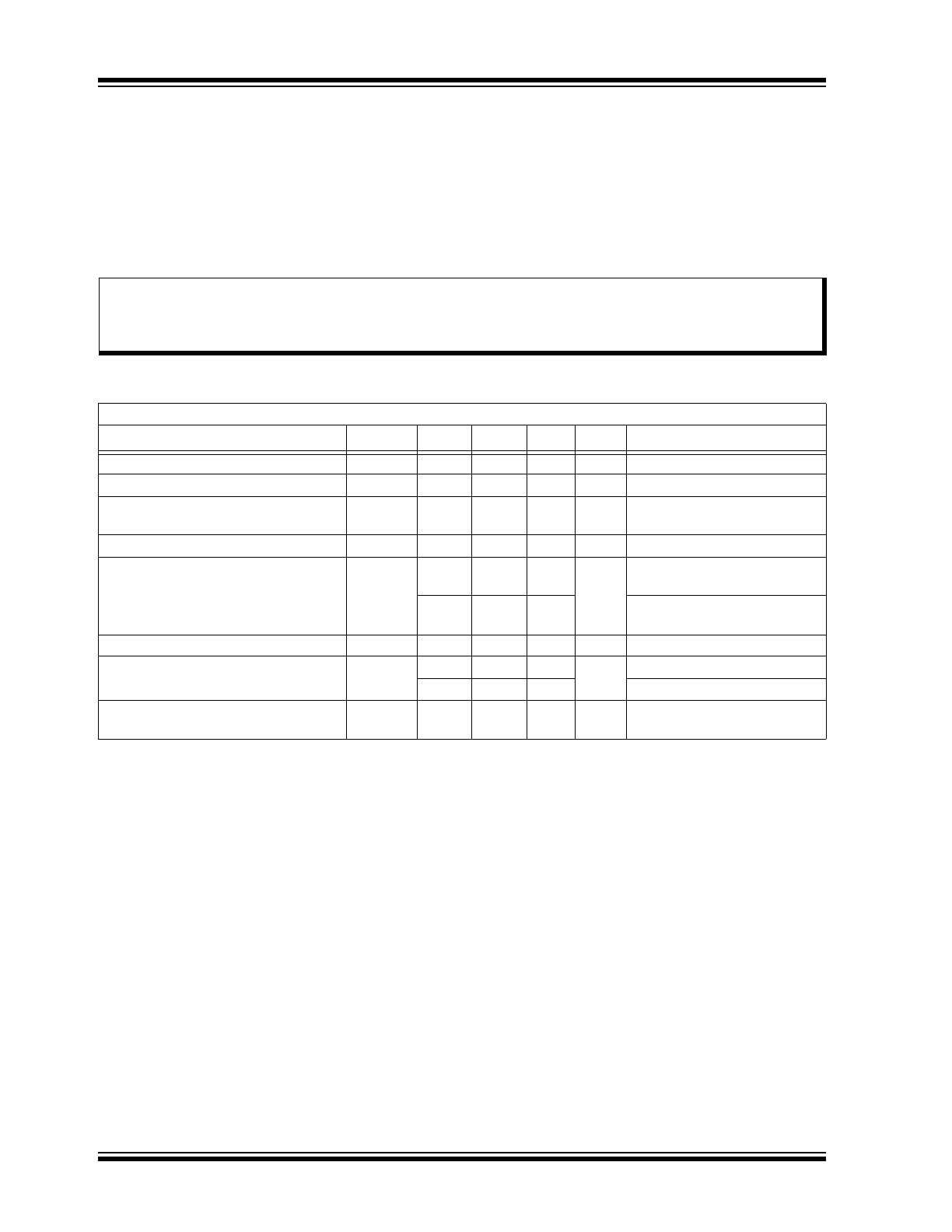
1.0
ELECTRICAL CHARACTERISTICS
Absolute Maximum Ratings†
Drain-to-Source Voltage ...................................................................................................................................... BV
DSS
Drain-to-Gate Voltage ......................................................................................................................................... BV
DGS
Gate-to-Source Voltage ......................................................................................................................................... ±30V
Operating Ambient Temperature, T
A
................................................................................................... –55°C to +150°C
Storage Temperature, T
S
..................................................................................................................... –55°C to +150°C
† Notice: Stresses above those listed under “Absolute Maximum Ratings” may cause permanent damage to the
device. This is a stress rating only, and functional operation of the device at those or any other conditions above those
indicated in the operational sections of this specification is not intended. Exposure to maximum rating conditions for
extended periods may affect device reliability.
DC ELECTRICAL CHARACTERISTICS
Electrical Specifications: T
A
= 25°C unless otherwise specified. (
Note 1
)
Parameter
Sym.
Min.
Typ.
Max.
Unit
Conditions
Drain-to-Source Breakdown Voltage
BV
DSS
60
—
—
V
V
GS
= 0V, I
D
= 10 µA
Gate Threshold Voltage
V
GS(th)
1
—
2.5
V
V
GS
= V
DS
, I
D
= 250 µA
Change in V
GS(th)
with Temperature
∆V
GS(th)
—
—
–5.5
mV/°C
V
GS
= V
DS
, I
D
= 250 µA
(
Note 2
)
Gate Body Leakage Current
I
GSS
—
—
±100
nA
V
GS
= ±20V, V
DS
= 0V
Zero-Gate Voltage Drain Current
I
DSS
—
—
1
µA
V
GS
= 0V, V
DS
= Maximum
Rating
—
—
500
V
GS
= 0V, V
DS
= 0.8 Maximum
Rating, T
A
= 125°C (
Note 2
)
On-State Drain Current
I
D(ON)
500
—
—
mA
V
GS
= 10V, V
DS
= 25V
Static Drain-to-Source On-State
Resistance
R
DS(ON)
—
—
7.5
Ω
V
GS
= 5V, I
D
= 50 mA
—
—
7.5
V
GS
= 10V, I
D
= 500 mA
Change in R
DS(ON)
with Temperature
∆
RDS(ON)
—
—
1
%/°C
V
GS
= 10V, I
D
= 500 mA
(
Note 2
)
Note 1: All DC parameters are 100% tested at 25°C unless otherwise stated.
(Pulse test: 300 µs pulse, 2% duty cycle)
2: Specification is obtained by characterization and is not 100% tested.
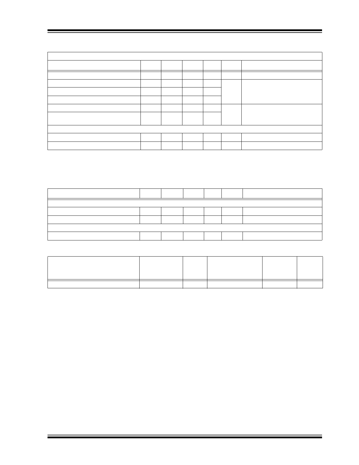
AC ELECTRICAL CHARACTERISTICS
Electrical Specifications: T
A
= 25°C unless otherwise specified. (
Note 2
)
Parameter
Sym.
Min.
Typ.
Max.
Unit
Conditions
Forward Transconductance
G
FS
80
—
—
mmho V
DS
= 25V, I
D
= 500 mA
Input Capacitance
C
ISS
—
—
50
pF
V
GS
= 0V,
V
DS
= 25V,
f = 1 MHz
Common Source Output Capacitance
C
OSS
—
—
25
Reverse Transfer Capacitance
C
RSS
—
—
5
Turn-On Time
t
(ON)
—
—
20
ns
V
DD
= 30V,
I
D
= 200 mA,
R
GEN
= 25Ω
Turn-Off Time
t
(OFF)
—
—
20
DIODE PARAMETER (
Note 2
)
Diode Forward Voltage Drop
V
SD
—
1.2
—
V
V
GS
= 0V, I
SD
= 200 mA (
Note 1
)
Reverse Recovery Time
t
rr
—
400
—
ns
V
GS
= 0V, I
SD
= 800 mA
Note 1: All DC parameters are 100% tested at 25°C unless otherwise stated.
(Pulse test: 300 µs pulse, 2% duty cycle)
2: Specification is obtained by characterization and is not 100% tested.
TEMPERATURE SPECIFICATIONS
Parameter
Sym.
Min.
Typ.
Max.
Unit
Conditions
TEMPERATURE RANGE
Operating Ambient Temperature
T
A
–55
—
+150
°C
Storage Temperature
T
S
–55
—
+150
°C
PACKAGE THERMAL RESISTANCE
3-lead SOT-23
JA
—
203
—
°C/W
THERMAL CHARACTERISTICS
Package
I
D
(
Note 1
)
(Continuous)
(mA)
I
D
(Pulsed)
(mA)
Power Dissipation at
T
A
= 25°C
(W)
I
DR
(
Note 1
)
(mA)
I
DRM
(mA)
3-lead SOT-23
115
800
0.36
115
800
Note 1: I
D
(continuous) is limited by maximum T
J
.
2018 Microchip Technology Inc.
DS20005797A-page 3
2N7002
2N7002
DS20005797A-page 4
2018 Microchip Technology Inc.
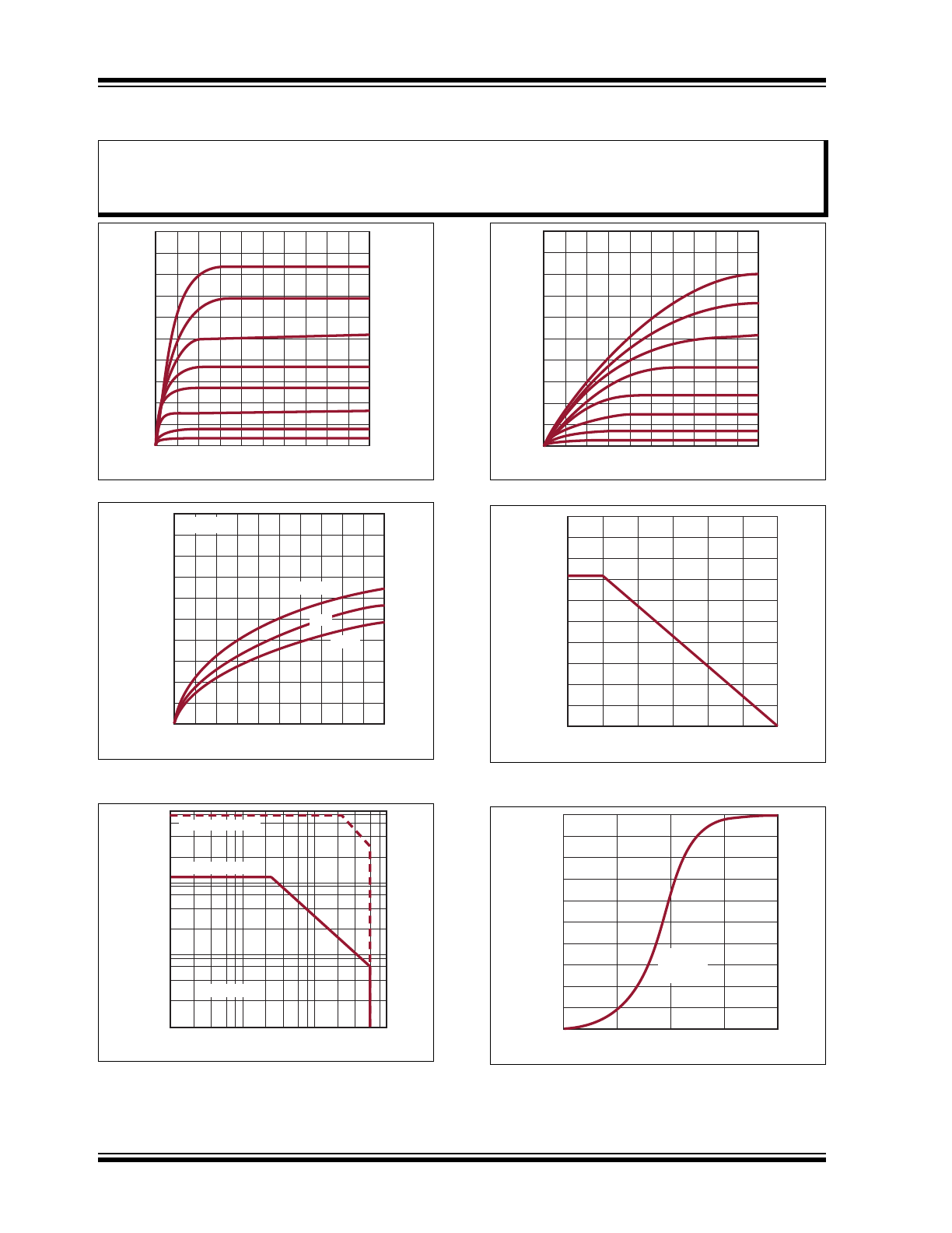
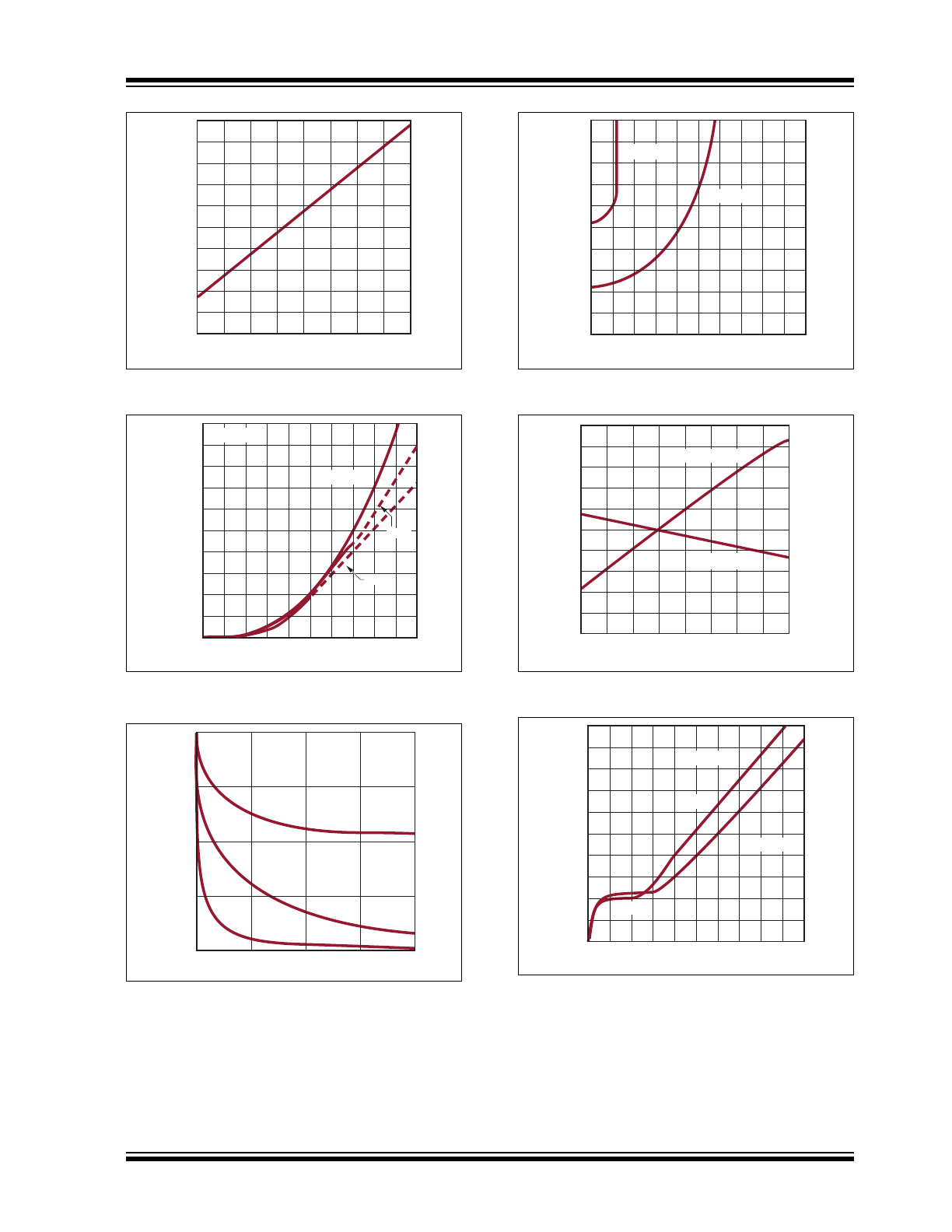
2.0
TYPICAL PERFORMANCE CURVES
2.0
1.6
1.2
0.8
0.4
0
0 10 20 30 40 50
4V
3V
7V
9V
8V
6V
5V
V
GS
= 10V
I
D
(amperes)
V
DS
(volts)
Note:
The graphs and tables provided following this note are a statistical summary based on a limited number of
samples and are provided for informational purposes only. The performance characteristics listed herein
are not tested or guaranteed. In some graphs or tables, the data presented may be outside the specified
operating range (e.g. outside specified power supply range) and therefore outside the warranted range.
FIGURE 2-1:
Output Characteristics.
0.5
0.4
0.3
0.2
0.1
0
0 0.2 0.4 0.6 0.8 10
T
A
= -55
O
C
V
DS
= 25V
25
O
C
125
O
C
G
FS
(seimens)
I
D
(amperes)
FIGURE 2-2:
Transconductance vs. Drain
Current.
0.1 1.0 10 100
1.0
0.1
0.01
0.001
T
A
= 25
O
C
SOT-23 (DC)
SOT-23 (pulsed)
V
DS
(volts)
I
D
(amperes)
FIGURE 2-3:
Maximum Rated Safe
Operating Area.
FIGURE 2-4:
Saturation Characteristics.
0 2 4 6 8 10
4V
3V
7V
9V
8V
6V
5V
V
DS
(volts)
I
D
(amperes)
V
GS
= 10V
2.0
1.6
1.2
0.8
0.4
0
0 25 50 75 100 125 150
SOT-23
P
D
(watts)
T
C
(
O
C)
0.5
0.4
0.3
0.2
0.1
0
FIGURE 2-5:
Power Dissipation vs. Case
Temperature.
1.0
0.8
0.6
0.4
0.2
0
0.001 0.01 0.1 1.0 10
SOT-23
T
A
= 25
O
C
P
D
= 0.36W
Thermal Resistance (normalized)
t
p
(seconds)
FIGURE 2-6:
Thermal Response
Characteristics.
2018 Microchip Technology Inc.
DS20005797A-page 5
2N7002
FIGURE 2-7:
-50 0 50 100 150
1.1
1.0
0.9
BV
DSS
(normalized)
T
j
(
O
C)
BV
DSS
Variation with
Temperature.
0 2 4 6 8 10
2.0
1.6
1.2
0.8
0.4
0
T
A
= -55
O
C
V
DS
= 25V
125
O
C
25
O
C
I
D
(amperes)
V
GS (volts)
FIGURE 2-8:
Transfer Characteristics.
50
25
0
0 10 20 30 40
f = 1.0MHz
C
ISS
C
OSS
C
RSS
C (picofarads)
V
DS
(volts)
FIGURE 2-9:
Capacitance vs.
Drain-to-Source Voltage.
FIGURE 2-10:
10
8
6
4
2
0
V
GS
= 5.0V
0 0.5 1.0 1.5 2.0 2.5
I
D
(amperes)
R
DSS(ON)
(ohms)
V
GS
= 10V
On-Resistance vs. Drain
Current.
1.4
1.2
1.0
0.8
0.6
2.0
1.6
1.2
0.8
0.4
0
V
GS(th)
@ 1.0mA
R
DS(ON)
@ 10V, 0.5A
V
GS(th)
(normalized)
R
DS(ON)
(normalized)
T
j
(
O
C)
-50 0 50 100 150
FIGURE 2-11:
V
GS(th)
and R
DS(ON)
Variation with Temperature.
10
8
6
4
2
0 0 0.2 0.4 0.6 0.8 1.0
30 pF
V
DS
= 40V
V
DS
= 10V
90 pF
Q
G
(nanocoulombs)
V
GS
(volts)
FIGURE 2-12:
Gate Drive Dynamic
Characteristics.
2N7002
DS20005797A-page 6
2018 Microchip Technology Inc.
3.0
PIN DESCRIPTION
Table 3-1
shows the description of pins in 2N7002.
Refer to
Package Type
for the location of pins.
TABLE 3-1:
PIN FUNCTION TABLE
Pin Number
Pin Name
Description
1
Gate
Gate
2
Source
Source
3
Drain
Drain
2018 Microchip Technology Inc.
DS20005797A-page 7
2N7002
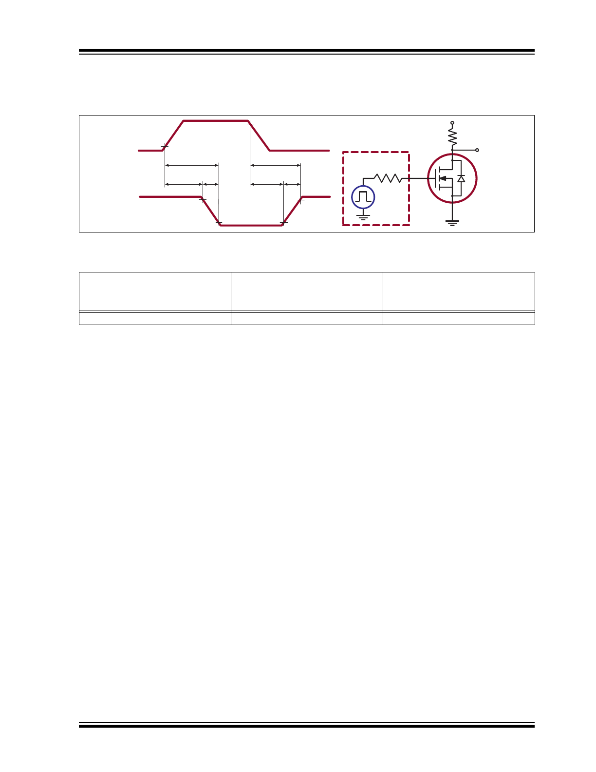
4.0
FUNCTIONAL DESCRIPTION
Figure 4-1
illustrates the switching waveforms and test
circuit for 2N7002.
90%
10%
90%
90%
10%
10%
Pulse
Generator
VDD
R
L
OUTPUT
D.U.T.
t
(ON)
t
d(ON)
t
(OFF)
t
d(OFF)
t
r
INPUT
INPUT
OUTPUT
10V
VDD
R
GEN
0V
0V
t
f
FIGURE 4-1:
Switching Waveforms and Test Circuit.
TABLE 4-1:
PRODUCT SUMMARY
BV
DSS
/BV
DGS
(V)
R
DS(ON)
(Maximum)
(Ω)
I
D(ON)
(Minimum)
(mA)
60
7.5
500
2N7002
DS20005797A-page 8
2018 Microchip Technology Inc.
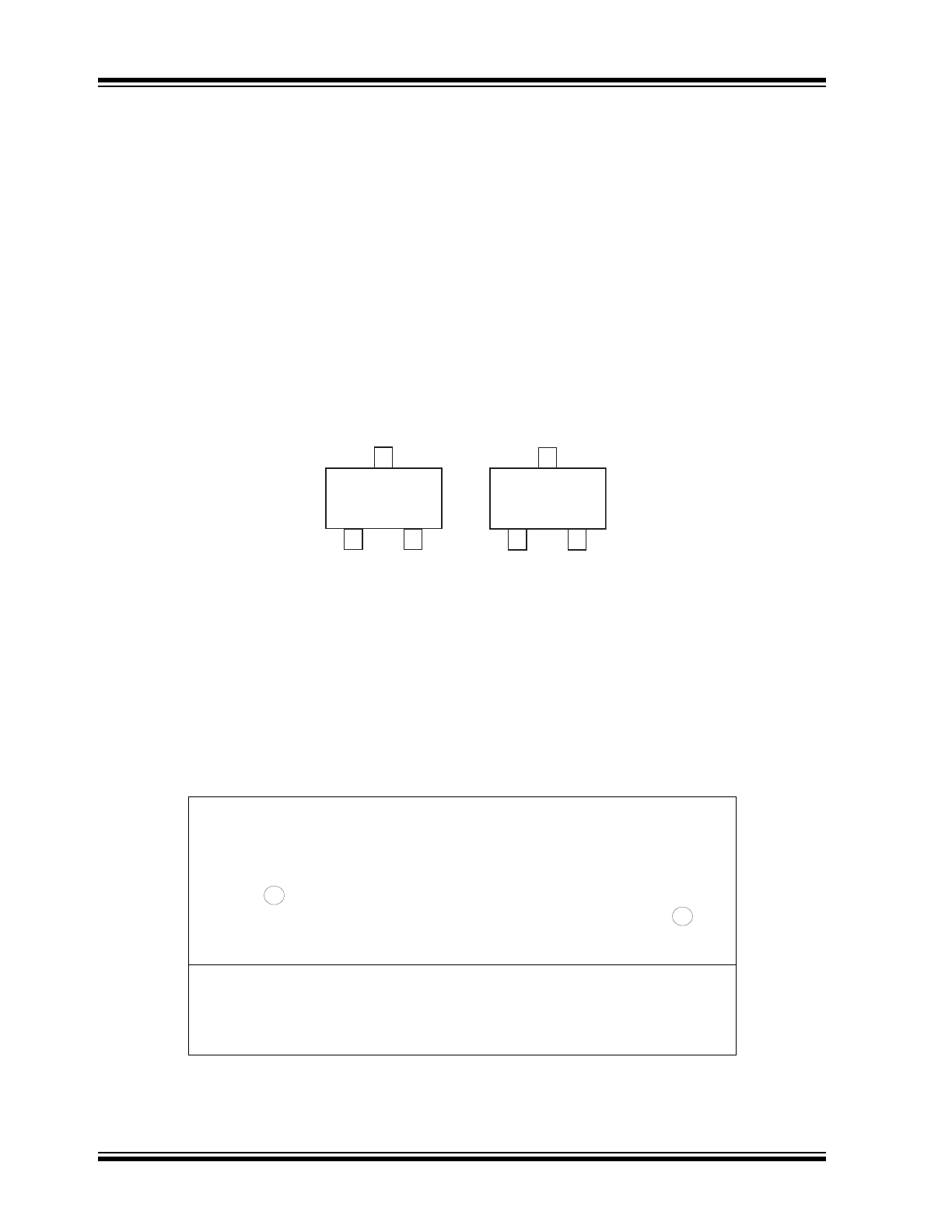
5.0
PACKAGING INFORMATION
5.1
Package Marking Information
Legend: XX...X
Product Code or Customer-specific information
Y
Year code (last digit of calendar year)
YY
Year code (last 2 digits of calendar year)
WW
Week code (week of January 1 is week ‘01’)
NNN
Alphanumeric traceability code
Pb-free JEDEC
®
designator for Matte Tin (Sn)
*
This package is Pb-free. The Pb-free JEDEC designator ( )
can be found on the outer packaging for this package.
Note:
In the event the full Microchip part number cannot be marked on one line, it will
be carried over to the next line, thus limiting the number of available
characters for product code or customer-specific information. Package may or
not include the corporate logo.
3
e
3
e
XXXNNN
702149
3-lead SOT-23
Example
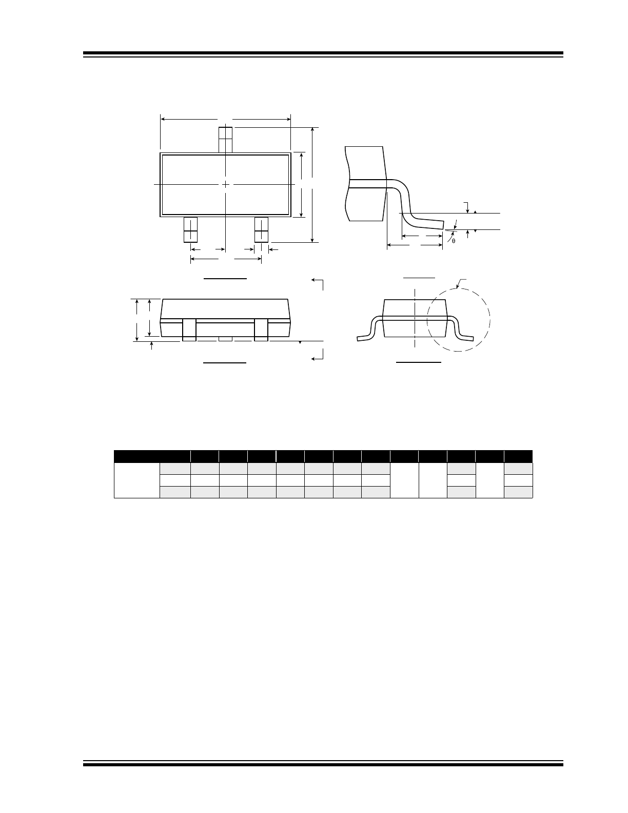
3-Lead TO-236AB (SOT-23) Package Outline (K1/T)
2.90x1.30mm body, 1.12mm height (max), 1.90mm pitch
Symbol
A
A1
A2
b
D
E
E1
e
e1
L
L1
ș
Dimension
(mm)
MIN
0.89
0.01
0.88
0.30
2.80
2.10
1.20
0.95
BSC
1.90
BSC
0.20
†
0.54
REF
0
O
NOM
-
-
0.95
-
2.90
-
1.30
0.50
-
MAX
1.12
0.10
1.02
0.50
3.04
2.64
1.40
0.60
8
O
JEDEC Registration TO-236, Variation AB, Issue H, Jan. 1999.
† This dimension differs from the JEDEC drawing.
Drawings not to scale.
View B
View A - A
Side View
Top View
View B
Gauge
Plane
Seating
Plane
0.25
L1
L
E1 E
D
3
1
2
e
e1
b
A
A
Seating
Plane
A
A2
A1
Note: For the most current package drawings, see the Microchip Packaging Specification at www.microchip.com/packaging.
Note: For the most current package drawings, see the Microchip Packaging Specification at www.microchip.com/packaging.
2018 Microchip Technology Inc.
DS20005797A-page 9
2N7002

2N7002
DS20005797A-page 10
2018 Microchip Technology Inc.
NOTES:
2018 Microchip Technology Inc.
DS20005797A-page 1
2N7002
Features
• Free from Secondary Breakdown
• Low Power Drive Requirement
• Ease of Paralleling
• Low C
ISS
and Fast Switching Speeds
• Excellent Thermal Stability
• Integral Source-Drain Diode
• High Input Impedance and High Gain
Applications
• Motor Controls
• Converters
• Amplifiers
• Switches
• Power Supply Circuits
• Drivers (Relays, Hammers, Solenoids, Lamps,
Memories, Displays, Bipolar Transistors, etc.)
General Description
The 2N7002 is a low-threshold, Enhancement-mode
(normally-off) transistor that uses a vertical DMOS
structure and a well-proven silicon-gate manufacturing
process. This combination produces a device with the
power handling capabilities of bipolar transistors and
the high input impedance and positive temperature
coefficient inherent in MOS devices. Characteristic of
all MOS structures, this device is free from thermal
runaway and thermally induced secondary breakdown.
Microchip’s vertical DMOS FETs are ideally suited to a
wide range of switching and amplifying applications
where very low threshold voltage, high breakdown
voltage, high input impedance, low input capacitance
and fast switching speeds are desired.
Package Type
3-lead SOT-23
(Top view)
See
Table 3-1
for pin information.
DRAIN
SOURCE
GATE
N-Channel Enhancement-Mode Vertical DMOS FET
2N7002
DS20005797A-page 2
2018 Microchip Technology Inc.
1.0
ELECTRICAL CHARACTERISTICS
Absolute Maximum Ratings†
Drain-to-Source Voltage ...................................................................................................................................... BV
DSS
Drain-to-Gate Voltage ......................................................................................................................................... BV
DGS
Gate-to-Source Voltage ......................................................................................................................................... ±30V
Operating Ambient Temperature, T
A
................................................................................................... –55°C to +150°C
Storage Temperature, T
S
..................................................................................................................... –55°C to +150°C
† Notice: Stresses above those listed under “Absolute Maximum Ratings” may cause permanent damage to the
device. This is a stress rating only, and functional operation of the device at those or any other conditions above those
indicated in the operational sections of this specification is not intended. Exposure to maximum rating conditions for
extended periods may affect device reliability.
DC ELECTRICAL CHARACTERISTICS
Electrical Specifications: T
A
= 25°C unless otherwise specified. (
Note 1
)
Parameter
Sym.
Min.
Typ.
Max.
Unit
Conditions
Drain-to-Source Breakdown Voltage
BV
DSS
60
—
—
V
V
GS
= 0V, I
D
= 10 µA
Gate Threshold Voltage
V
GS(th)
1
—
2.5
V
V
GS
= V
DS
, I
D
= 250 µA
Change in V
GS(th)
with Temperature
∆V
GS(th)
—
—
–5.5
mV/°C
V
GS
= V
DS
, I
D
= 250 µA
(
Note 2
)
Gate Body Leakage Current
I
GSS
—
—
±100
nA
V
GS
= ±20V, V
DS
= 0V
Zero-Gate Voltage Drain Current
I
DSS
—
—
1
µA
V
GS
= 0V, V
DS
= Maximum
Rating
—
—
500
V
GS
= 0V, V
DS
= 0.8 Maximum
Rating, T
A
= 125°C (
Note 2
)
On-State Drain Current
I
D(ON)
500
—
—
mA
V
GS
= 10V, V
DS
= 25V
Static Drain-to-Source On-State
Resistance
R
DS(ON)
—
—
7.5
Ω
V
GS
= 5V, I
D
= 50 mA
—
—
7.5
V
GS
= 10V, I
D
= 500 mA
Change in R
DS(ON)
with Temperature
∆
RDS(ON)
—
—
1
%/°C
V
GS
= 10V, I
D
= 500 mA
(
Note 2
)
Note 1: All DC parameters are 100% tested at 25°C unless otherwise stated.
(Pulse test: 300 µs pulse, 2% duty cycle)
2: Specification is obtained by characterization and is not 100% tested.
AC ELECTRICAL CHARACTERISTICS
Electrical Specifications: T
A
= 25°C unless otherwise specified. (
Note 2
)
Parameter
Sym.
Min.
Typ.
Max.
Unit
Conditions
Forward Transconductance
G
FS
80
—
—
mmho V
DS
= 25V, I
D
= 500 mA
Input Capacitance
C
ISS
—
—
50
pF
V
GS
= 0V,
V
DS
= 25V,
f = 1 MHz
Common Source Output Capacitance
C
OSS
—
—
25
Reverse Transfer Capacitance
C
RSS
—
—
5
Turn-On Time
t
(ON)
—
—
20
ns
V
DD
= 30V,
I
D
= 200 mA,
R
GEN
= 25Ω
Turn-Off Time
t
(OFF)
—
—
20
DIODE PARAMETER (
Note 2
)
Diode Forward Voltage Drop
V
SD
—
1.2
—
V
V
GS
= 0V, I
SD
= 200 mA (
Note 1
)
Reverse Recovery Time
t
rr
—
400
—
ns
V
GS
= 0V, I
SD
= 800 mA
Note 1: All DC parameters are 100% tested at 25°C unless otherwise stated.
(Pulse test: 300 µs pulse, 2% duty cycle)
2: Specification is obtained by characterization and is not 100% tested.
TEMPERATURE SPECIFICATIONS
Parameter
Sym.
Min.
Typ.
Max.
Unit
Conditions
TEMPERATURE RANGE
Operating Ambient Temperature
T
A
–55
—
+150
°C
Storage Temperature
T
S
–55
—
+150
°C
PACKAGE THERMAL RESISTANCE
3-lead SOT-23
JA
—
203
—
°C/W
THERMAL CHARACTERISTICS
Package
I
D
(
Note 1
)
(Continuous)
(mA)
I
D
(Pulsed)
(mA)
Power Dissipation at
T
A
= 25°C
(W)
I
DR
(
Note 1
)
(mA)
I
DRM
(mA)
3-lead SOT-23
115
800
0.36
115
800
Note 1: I
D
(continuous) is limited by maximum T
J
.
2018 Microchip Technology Inc.
DS20005797A-page 3
2N7002
2N7002
DS20005797A-page 4
2018 Microchip Technology Inc.
2.0
TYPICAL PERFORMANCE CURVES
2.0
1.6
1.2
0.8
0.4
0
0 10 20 30 40 50
4V
3V
7V
9V
8V
6V
5V
V
GS
= 10V
I
D
(amperes)
V
DS
(volts)
Note:
The graphs and tables provided following this note are a statistical summary based on a limited number of
samples and are provided for informational purposes only. The performance characteristics listed herein
are not tested or guaranteed. In some graphs or tables, the data presented may be outside the specified
operating range (e.g. outside specified power supply range) and therefore outside the warranted range.
FIGURE 2-1:
Output Characteristics.
0.5
0.4
0.3
0.2
0.1
0
0 0.2 0.4 0.6 0.8 10
T
A
= -55
O
C
V
DS
= 25V
25
O
C
125
O
C
G
FS
(seimens)
I
D
(amperes)
FIGURE 2-2:
Transconductance vs. Drain
Current.
0.1 1.0 10 100
1.0
0.1
0.01
0.001
T
A
= 25
O
C
SOT-23 (DC)
SOT-23 (pulsed)
V
DS
(volts)
I
D
(amperes)
FIGURE 2-3:
Maximum Rated Safe
Operating Area.
FIGURE 2-4:
Saturation Characteristics.
0 2 4 6 8 10
4V
3V
7V
9V
8V
6V
5V
V
DS
(volts)
I
D
(amperes)
V
GS
= 10V
2.0
1.6
1.2
0.8
0.4
0
0 25 50 75 100 125 150
SOT-23
P
D
(watts)
T
C
(
O
C)
0.5
0.4
0.3
0.2
0.1
0
FIGURE 2-5:
Power Dissipation vs. Case
Temperature.
1.0
0.8
0.6
0.4
0.2
0
0.001 0.01 0.1 1.0 10
SOT-23
T
A
= 25
O
C
P
D
= 0.36W
Thermal Resistance (normalized)
t
p
(seconds)
FIGURE 2-6:
Thermal Response
Characteristics.
2018 Microchip Technology Inc.
DS20005797A-page 5
2N7002
FIGURE 2-7:
-50 0 50 100 150
1.1
1.0
0.9
BV
DSS
(normalized)
T
j
(
O
C)
BV
DSS
Variation with
Temperature.
0 2 4 6 8 10
2.0
1.6
1.2
0.8
0.4
0
T
A
= -55
O
C
V
DS
= 25V
125
O
C
25
O
C
I
D
(amperes)
V
GS (volts)
FIGURE 2-8:
Transfer Characteristics.
50
25
0
0 10 20 30 40
f = 1.0MHz
C
ISS
C
OSS
C
RSS
C (picofarads)
V
DS
(volts)
FIGURE 2-9:
Capacitance vs.
Drain-to-Source Voltage.
FIGURE 2-10:
10
8
6
4
2
0
V
GS
= 5.0V
0 0.5 1.0 1.5 2.0 2.5
I
D
(amperes)
R
DSS(ON)
(ohms)
V
GS
= 10V
On-Resistance vs. Drain
Current.
1.4
1.2
1.0
0.8
0.6
2.0
1.6
1.2
0.8
0.4
0
V
GS(th)
@ 1.0mA
R
DS(ON)
@ 10V, 0.5A
V
GS(th)
(normalized)
R
DS(ON)
(normalized)
T
j
(
O
C)
-50 0 50 100 150
FIGURE 2-11:
V
GS(th)
and R
DS(ON)
Variation with Temperature.
10
8
6
4
2
0 0 0.2 0.4 0.6 0.8 1.0
30 pF
V
DS
= 40V
V
DS
= 10V
90 pF
Q
G
(nanocoulombs)
V
GS
(volts)
FIGURE 2-12:
Gate Drive Dynamic
Characteristics.
2N7002
DS20005797A-page 6
2018 Microchip Technology Inc.
3.0
PIN DESCRIPTION
Table 3-1
shows the description of pins in 2N7002.
Refer to
Package Type
for the location of pins.
TABLE 3-1:
PIN FUNCTION TABLE
Pin Number
Pin Name
Description
1
Gate
Gate
2
Source
Source
3
Drain
Drain
2018 Microchip Technology Inc.
DS20005797A-page 7
2N7002
4.0
FUNCTIONAL DESCRIPTION
Figure 4-1
illustrates the switching waveforms and test
circuit for 2N7002.
90%
10%
90%
90%
10%
10%
Pulse
Generator
VDD
R
L
OUTPUT
D.U.T.
t
(ON)
t
d(ON)
t
(OFF)
t
d(OFF)
t
r
INPUT
INPUT
OUTPUT
10V
VDD
R
GEN
0V
0V
t
f
FIGURE 4-1:
Switching Waveforms and Test Circuit.
TABLE 4-1:
PRODUCT SUMMARY
BV
DSS
/BV
DGS
(V)
R
DS(ON)
(Maximum)
(Ω)
I
D(ON)
(Minimum)
(mA)
60
7.5
500
2N7002
DS20005797A-page 8
2018 Microchip Technology Inc.
5.0
PACKAGING INFORMATION
5.1
Package Marking Information
Legend: XX...X
Product Code or Customer-specific information
Y
Year code (last digit of calendar year)
YY
Year code (last 2 digits of calendar year)
WW
Week code (week of January 1 is week ‘01’)
NNN
Alphanumeric traceability code
Pb-free JEDEC
®
designator for Matte Tin (Sn)
*
This package is Pb-free. The Pb-free JEDEC designator ( )
can be found on the outer packaging for this package.
Note:
In the event the full Microchip part number cannot be marked on one line, it will
be carried over to the next line, thus limiting the number of available
characters for product code or customer-specific information. Package may or
not include the corporate logo.
3
e
3
e
XXXNNN
702149
3-lead SOT-23
Example
3-Lead TO-236AB (SOT-23) Package Outline (K1/T)
2.90x1.30mm body, 1.12mm height (max), 1.90mm pitch
Symbol
A
A1
A2
b
D
E
E1
e
e1
L
L1
ș
Dimension
(mm)
MIN
0.89
0.01
0.88
0.30
2.80
2.10
1.20
0.95
BSC
1.90
BSC
0.20
†
0.54
REF
0
O
NOM
-
-
0.95
-
2.90
-
1.30
0.50
-
MAX
1.12
0.10
1.02
0.50
3.04
2.64
1.40
0.60
8
O
JEDEC Registration TO-236, Variation AB, Issue H, Jan. 1999.
† This dimension differs from the JEDEC drawing.
Drawings not to scale.
View B
View A - A
Side View
Top View
View B
Gauge
Plane
Seating
Plane
0.25
L1
L
E1 E
D
3
1
2
e
e1
b
A
A
Seating
Plane
A
A2
A1
Note: For the most current package drawings, see the Microchip Packaging Specification at www.microchip.com/packaging.
Note: For the most current package drawings, see the Microchip Packaging Specification at www.microchip.com/packaging.
2018 Microchip Technology Inc.
DS20005797A-page 9
2N7002
2N7002
DS20005797A-page 10
2018 Microchip Technology Inc.
NOTES: