
©
2005 Microchip Technology Inc.
DS21874B-page 1
MCP1701
Features
• 2.0 µA Typical Quiescent Current
• Input Operating Voltage Range up to 10.0V
• Low Dropout Voltage:
- 250 mV (typ) @ 100 mA
- 500 mV (typ) @ 200 mA
• High Output Current: 250 mA (V
OUT
= 5.0V)
• High-Accuracy Output Voltage: ±2% (max)
• Low Temperature Drift: ±100 ppm/°C (typ.)
• Excellent Line Regulation: 0.2%/V (typ.)
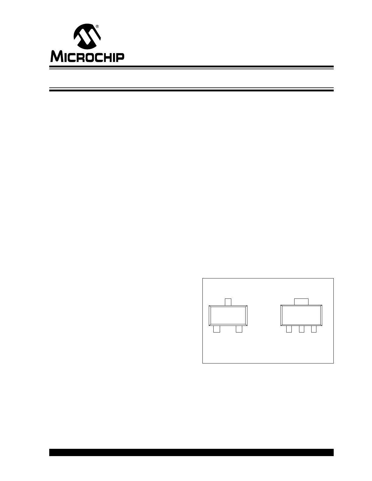
• Package Options: 3-Pin SOT-23A and
3-Pin SOT-89
• Short Circuit Protection
• Standard Output Voltage Options:
- 1.8V, 2.5V, 3.0V, 3.3V, 5.0V
Applications
• Battery-Powered Devices
• Battery-Powered Alarm Circuits
• Smoke Detectors
• CO
2
Detectors
• Smart Battery Packs
• PDAs
• Low Quiescent Current Voltage Reference
• Cameras and Portable Video Equipment
• Pagers and Cellular Phones
• Solar-Powered Instruments
• Consumer Products
• Microcontroller Power
Related Literature
• AN765, “Using Microchip’s Micropower LDOs”,
DS00765, Microchip Technology Inc., 2002
• AN766, “Pin-Compatible CMOS Upgrades to
Bipolar LDOs”, DS00766, Microchip Technology
Inc., 2002
General Description
The MCP1701 is a family of CMOS low dropout (LDO),
positive voltage regulators that can deliver up to
250 mA of current while consuming only 2.0 µA of
quiescent current (typ.). The input operating range is
specified up to 10V, making it ideal for lithium-ion (one
or two cells), 9V alkaline and other two and three
primary cell battery-powered applications.
The MCP1701 is capable of delivering 250 mA with an
input-to-output voltage differential (dropout voltage) of
650 mV. The low dropout voltage extends the battery
operating lifetime. It also permits high currents in small
packages when operated with minimum V
IN
– V
OUT
differentials.
The MCP1701 has a tight tolerance output voltage
regulation of ±0.5% (typ.) and very good line regulation
at ±0.2%. The LDO output is stable when using only
1 µF of output capacitance of either tantalum or
aluminum-electrolytic style capacitors. The MCP1701
LDO also incorporates short circuit protection to ensure
maximum reliability.
Package options include the 3-pin SOT-23A and 3-pin
SOT-89.
Package Types
V
IN
GND
V
OUT
3
1
2
MCP1701
GND V
IN
V
OUT
1
2
3
MCP1701
3-Pin SOT-23A
3-Pin SOT-89
V
IN
Note: 3-Pin SOT-23A is equivalent to the EIAJ
SC-59.
2 µA Low Dropout Positive Voltage Regulator
MCP1701
DS21874B-page 2
©
2005 Microchip Technology Inc.
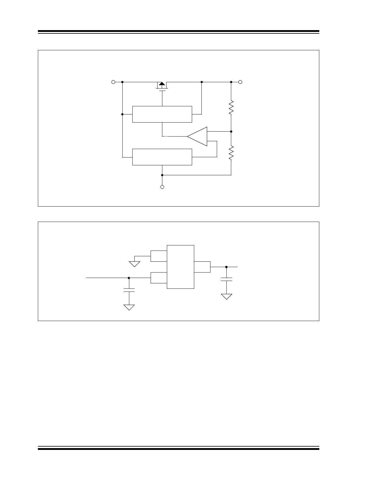
Functional Block Diagram
Typical Application Circuits
V
IN
V
OUT
GND
Short-Circuit
Protection
Voltage
Reference
+
–
MCP1701
MCP1701
GND
V
OUT
V
IN
C
IN
1 µF Tantalum
C
OUT
1 µF Tantalum
V
OUT
V
IN
3.3V
I
OUT
50 mA
9V Alkaline Battery
©
2005 Microchip Technology Inc.
DS21874B-page 3
MCP1701
1.0
ELECTRICAL
CHARACTERISTICS
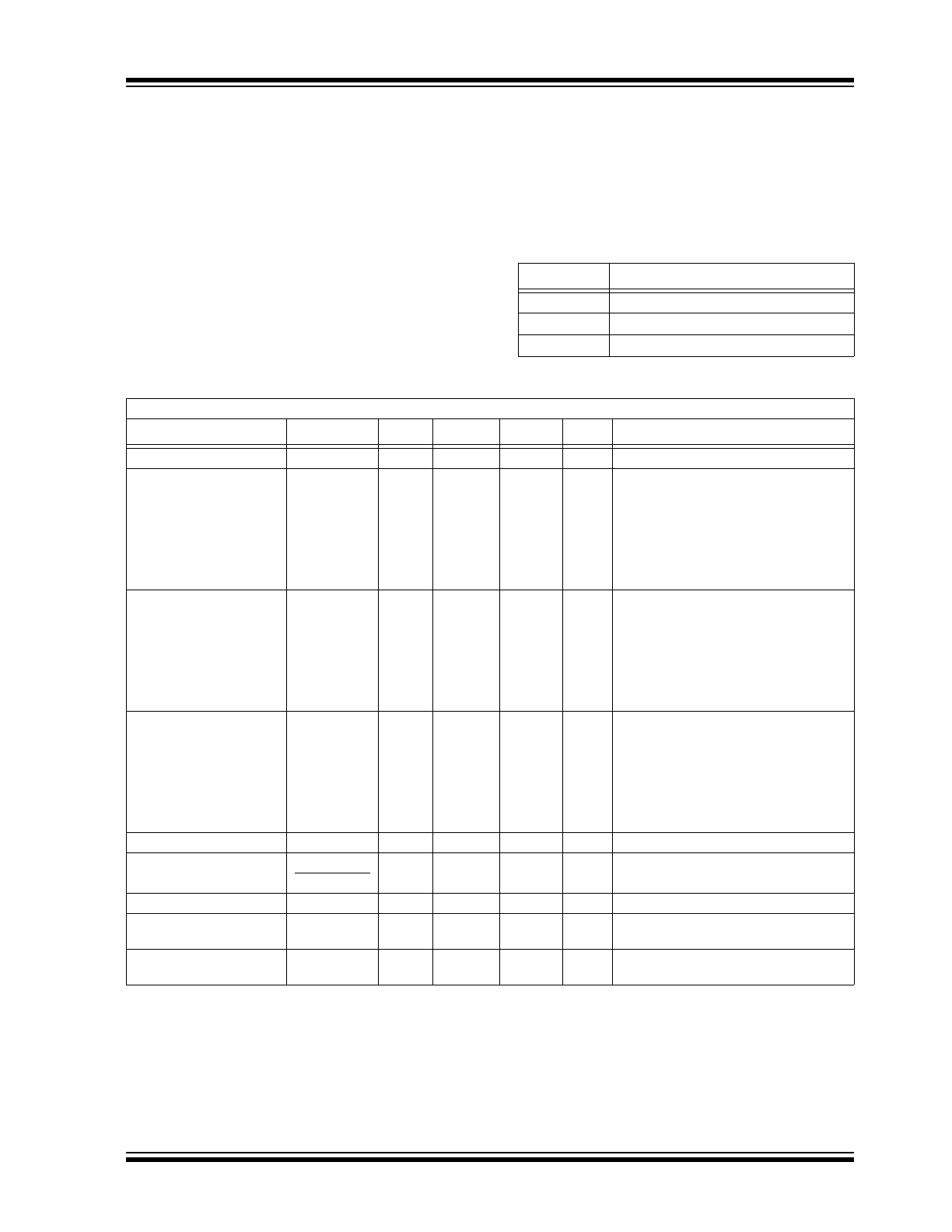
Absolute Maximum Ratings †
Input Voltage ........................................................ +12V
Output Current (Continuous)..........P
D
/(V
IN
– V
OUT
)mA
Output Current (peak) ..................................... 500 mA
Output Voltage ............... (GND – 0.3V) to (V
IN
+ 0.3V)
Continuous Power Dissipation:
3-Pin SOT-23A ............................................ 150 mW
3-Pin SOT-89............................................... 500 mW
† Notice: Stresses above those listed under “Absolute
Maximum Ratings” may cause permanent damage to the
device. These are stress ratings only and functional operation
of the device at these or any other conditions above those
indicated in the operation sections of the specifications is not
implied. Exposure to Absolute Maximum Rating conditions for
extended periods may affect device reliability.
PIN FUNCTION TABLE
Symbol
Description
GND
Ground Terminal
V
OUT
Regulated Voltage Output
V
IN
Unregulated Supply Input
ELECTRICAL CHARACTERISTICS
Electrical Specifications: Unless otherwise specified, all limits are established for an ambient temperature of T
A
= +25°C.
Parameters
Sym
Min
Typ
Max
Units
Conditions
Output Voltage Regulation
V
OUT
V
R
- 2%
V
R
±0.5%
V
R
+ 2%
V
I
OUT
= 40 mA (Note 1)
Maximum Output Current
I
OUT
MAX
250
—
—
mA
V
OUT
= 5.0V (V
IN
= V
R
+ 1.0V)
200
—
—
V
OUT
= 4.0V
150
—
—
V
OUT
= 3.3V
150
—
—
V
OUT
= 3.0V
125
—
—
V
OUT
= 2.5V
110
—
—
V
OUT
= 1.8V
Load Regulation (Note 3)
Δ
V
OUT/
V
OUT
-1.60
±0.8
+1.60
%
V
OUT
= 5.0V, 1 mA
≤
I
OUT
≤
100 mA
-2.25
±1.1
+2.25
V
OUT
= 4.0V, 1 mA
≤
I
OUT
≤
100 mA
-2.72
±1.3
+2.72
V
OUT
= 3.3V, 1 mA
≤
I
OUT
≤
80 mA
-3.00
±1.5
+3.00
V
OUT
= 3.0V, 1 mA
≤
I
OUT
≤
80 mA
-3.60
±1.8
+3.60
V
OUT
= 2.5V, 1 mA
≤
I
OUT
≤
60 mA
-1.60
±0.8
+1.60
V
OUT
= 1.8V, 1 mA
≤
I
OUT
≤
30 mA
Dropout Voltage
V
IN
- V
OUT
—
400
630
mV
I
OUT
= 200 mA, V
R
= 5.0V
—
400
630
I
OUT
= 200 mA, V
R
= 4.0V
—
400
700
I
OUT
= 160 mA, V
R
= 3.3V
—
400
700
I
OUT
= 160 mA, V
R
= 3.0V
—
400
700
I
OUT
= 120 mA, V
R
= 2.5V
—
180
300
I
OUT
= 20 mA, V
R
= 1.8V
Input Quiescent Current
I
Q
—
2.0
3.0
µA
V
IN
= V
R
+ 1.0V
Line Regulation
Δ
V
OUT
•100
Δ
V
IN
•V
OUT
—
0.2
0.3
%/V
I
OUT
= 40 mA, (V
R
+1)
≤
V
IN
≤
10.0V
Input Voltage
V
IN
—
—
10
V
Temperature Coefficient of
Output Voltage
TCV
OUT
—
±100
—
ppm/°
C
I
OUT
= 40 mA, -40°C
≤
T
A
≤ +
85°C
(Note 2)
Output Rise Time
T
R
—
200
—
µsec
10% V
R
to 90% V
R
, V
IN
= 0V to V
R
+1V,
R
L
= 25
Ω
resistive
1:
V
R
is the nominal regulator output voltage. For example: V
R
= 1.8V, 2.5V, 3.3V, 4.0V, 5.0V.
The input voltage V
IN
= V
R
+ 1.0V, I
OUT
= 40 mA.
2:
TCV
OUT
= (V
OUT-HIGH
– V
OUT-LOW
) *10
6
/ (V
R
*
Δ
Temperature), V
OUT-HIGH
= Highest voltage measured
over the temperature range. V
OUT-LOW
= Lowest voltage measured over the temperature range.
3:
Load regulation is measured at a constant junction temperature using low duty cycle pulse testing.
MCP1701
DS21874B-page 4
©
2005 Microchip Technology Inc.
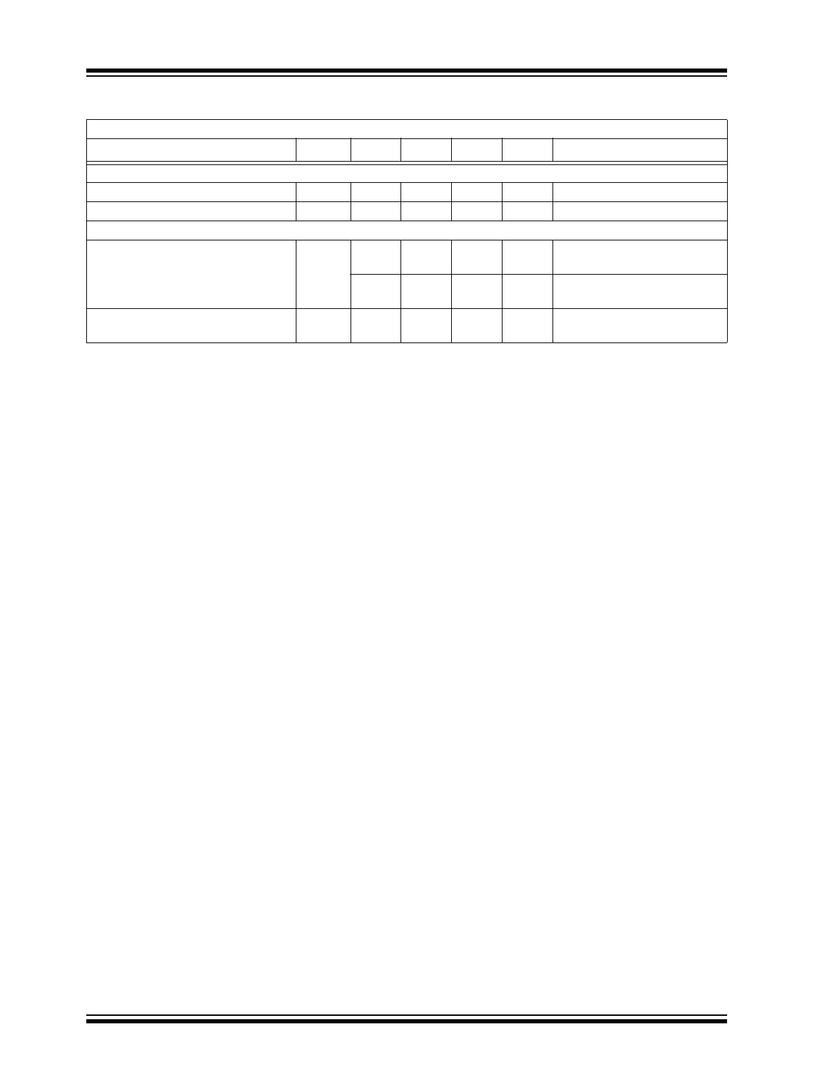
TEMPERATURE CHARACTERISTICS
Electrical Specifications: Unless otherwise specified,
T
A
= +25
°C.
Parameters
Sym
Min
Typ
Max
Units
Conditions
Temperature Ranges
Specified Temperature Range (I)
T
A
-40
—
+85
°C
Storage Temperature Range
T
A
-40
—
+125
°C
Package Thermal Resistances
Thermal Resistance, 3L-SOT-23A
θ
JA
—
335
—
°C/W
Minimum trace width single
layer application
—
230
—
°C/W
Typical FR4, 4-layer
application
Thermal Resistance, 3L-SOT-89
θ
JA
—
52
—
°C/W
Typical, when mounted on 1
square inch of copper
©
2005 Microchip Technology Inc.
DS21874B-page 5
MCP1701
2.0
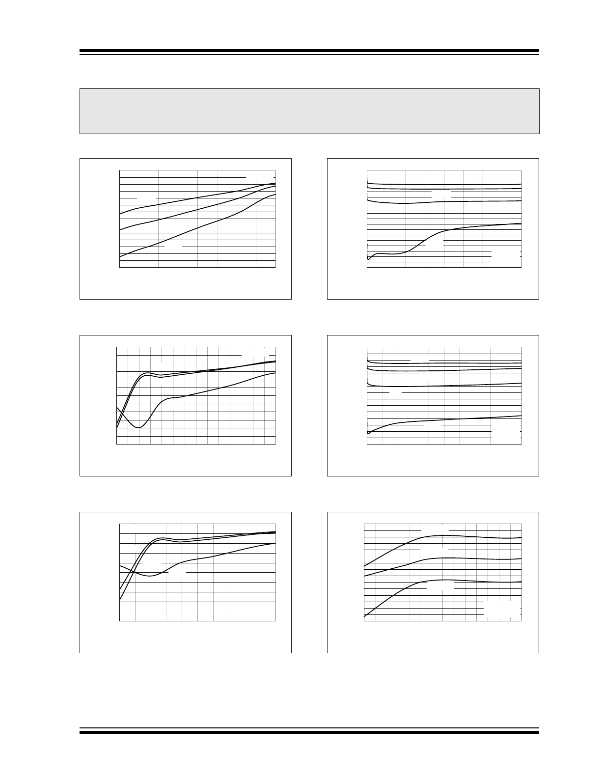
TYPICAL PERFORMANCE CURVES
Notes: Unless otherwise specified, V
OUT
= 1.8V, 3.0V, 5.0V, T
A
= +25°C, C
IN
= 1 µF Tantalum, C
OUT
= 1 µF Tantalum.
FIGURE 2-1:
Supply Current vs. Input
Voltage (V
R
= 1.8V).
FIGURE 2-2:
Supply Current vs. Input
Voltage (V
R
= 3.0V).
FIGURE 2-3:
Supply Current vs. Input
Voltage (V
R
= 5.0V).
FIGURE 2-4:
Supply Current vs. Load
Current (V
R
= 3.0V).
FIGURE 2-5:
Supply Current vs. Load
Current (V
R
= 5.0V).
FIGURE 2-6:
Supply Current vs.
Temperature.
Note:
The graphs and tables provided following this note are a statistical summary based on a limited number of
samples and are provided for informational purposes only. The performance characteristics listed herein
are not tested or guaranteed. In some graphs or tables, the data presented may be outside the specified
operating range (e.g., outside specified power supply range) and therefore outside the warranted range.
1.95
2.00
2.05
2.10
2.15
2.20
2.25
2.30
2.35
2.40
2.45
2.50
2.55
2.60
2.65
2
3
4
5
6
7
8
9
10
Input Voltage (V)
S
uppl
y C
u
rr
e
nt (
µ
A)
V
R
= 1.8V
-40°C
0°C
+25°C
1.2
1.3
1.4
1.5
1.6
1.7
1.8
1.9
2.0
2.1
2.2
2.3
2.4
3
4
5
6
7
8
9
10
Input Voltage (V)
S
uppl
y C
u
rr
e
nt (µ
A
)
-40°C
+85°C
+25°C
V
R
= 3.0V
1.50
1.65
1.80
1.95
2.10
2.25
2.40
2.55
2.70
2.85
3.00
5
6
7
8
9
10
Input Voltage (V)
S
uppl
y C
u
rr
e
nt (µ
A
)
-40°C
+85°C
+25°C
V
R
= 5.0V
1.20
1.25
1.30
1.35
1.40
1.45
1.50
1.55
1.60
1.65
1.70
1.75
1.80
1.85
1.90
1.95
2.00
2.05
2.10
0
20
40
60
80
100
120
140
160
Load Current (mA)
S
uppl
y C
u
rr
e
nt (µ
A
)
V
IN
= 4.0V
V
R
= 3.0V
+25°C
0°C
+85°C
-40°C
2.00
2.05
2.10
2.15
2.20
2.25
2.30
2.35
2.40
2.45
2.50
2.55
2.60
2.65
2.70
2.75
0
20
40
60
80
100
120
140
160
180
200
Load Current (mA)
S
uppl
y C
u
rr
e
nt (µ
A
)
-40°C
+25°C
+85°C
0°C
V
IN
= 6.0V
V
R
= 5.0V
1.4
1.5
1.6
1.7
1.8
1.9
2.0
2.1
2.2
2.3
2.4
2.5
2.6
2.7
2.8
2.9
-40
-20
0
20
40
60
80
100
Temperature (°C)
S
uppl
y C
u
rr
e
nt (µ
A
)
V
R
= 5.0V
V
R
= 1.8V
V
R
= 3.0V
V
IN
= V
R
+ 1V
I
OUT
= 0 µA
MCP1701
DS21874B-page 6
©
2005 Microchip Technology Inc.
Note: Unless otherwise indicated, V
OUT
= 1.8V, 3.0V, 5.0V, T
A
= +25°C, C
IN
= 1 µF Tantalum, C
OUT
= 1 µF Tantalum.
FIGURE 2-7:
Output Voltage vs. Input
Voltage (V
R
= 1.8V).
FIGURE 2-8:
Output Voltage vs. Input
Voltage (V
R
= 3.0V).
FIGURE 2-9:
Output Voltage vs. Input
Voltage (V
R
= 5.0V).
FIGURE 2-10:
Output Voltage vs. Load
Current (V
R
= 1.8V).
FIGURE 2-11:
Output Voltage vs. Load
Current (V
R
= 3.0V).
FIGURE 2-12:
Output Voltage vs. Load
Current (V
R
= 5.0V).
1.78
1.79
1.80
1.81
1.82
1.83
1.84
1.85
2
3
4
5
6
7
8
9
10
Input Voltage (V)
Output V
o
ltage (V
)
+85°C
+25°C
-40°C
I
OUT
= 0.1 mA
0°C
2.97
2.98
2.99
3.00
3.01
3.02
3.03
3.04
3.05
4.0
5.0
6.0
7.0
8.0
9.0
10.0
Input Voltage (V)
Output V
o
ltage (V
)
+25°C
+85°C
0°C
-40°C
I
OUT
= 0.1 mA
4.96
4.97
4.98
4.99
5.00
5.01
5.02
5.03
5.04
5.05
5.06
5.07
5.08
5.09
5.10
5.5
6.0
6.5
7.0
7.5
8.0
8.5
9.0
9.5
10.0
Input Voltage (V)
Output V
o
ltage (V
)
-40°C
+85°C
+25°C
I
OUT
= 0.1 mA
0°C
1.77
1.78
1.79
1.80
1.81
1.82
1.83
0
10
20
30
40
50
60
70
80
90
Load Current (mA)
Output V
o
ltage (V
)
+85°C
-40°C
0°C
V
IN
= 2.8V
+25°C
2.94
2.96
2.98
3.00
3.02
3.04
3.06
0
15
30
45
60
75
90
105
120
135
150
Load Current (mA)
Output V
o
ltage (V
)
-40°C
+85°C
0°C
V
IN
= 4.0V
+25°C
4.93
4.95
4.97
4.99
5.01
5.03
5.05
5.07
0
25
50
75
100
125
150
175
200
225
250
Load Current (mA)
Output V
o
ltage (V
)
-40°C
+25°C
0°C
+85°C
V
IN
= 6.0V
©
2005 Microchip Technology Inc.
DS21874B-page 7
MCP1701
Note: Unless otherwise indicated, V
OUT
= 1.8V, 3.0V, 5.0V, T
A
= +25°C, C
IN
= 1 µF Tantalum, C
OUT
= 1 µF Tantalum.
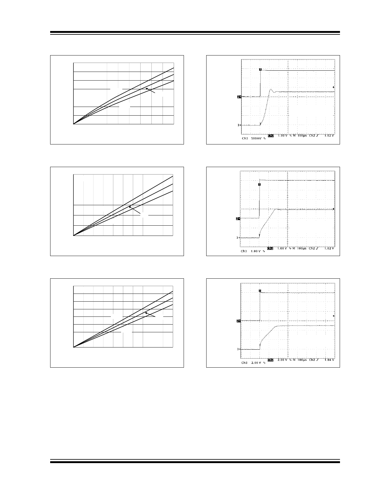
FIGURE 2-13:
Dropout Voltage vs. Load
Current (V
R
= 1.8V).
0
FIGURE 2-14:
Dropout Voltage vs. Load
Current (V
R
= 3.0V).
FIGURE 2-15:
Dropout Voltage vs. Load
Current (V
R
= 5.0V).
FIGURE 2-16:
Start-up From V
IN
(V
R
= 1.8V).
FIGURE 2-17:
Start-up From V
IN
(V
R
= 3.0V).
FIGURE 2-18:
Start-up From V
IN
(V
R
= 5.0V).
0.0
0.1
0.2
0.3
0.4
0.5
0.6
0.7
0
10
20
30
40
50
60
70
80
90
Load Current (mA)
D
ropout V
o
lt
age (V
)
-40°C
0°C
+85°C
V
R
= 1.8V
0
0.1
0.2
0.3
0.4
0.5
0.6
0
15
30
45
60
75
90
105
120
135
150
Load Current (mA)
D
ropout V
o
lt
age (V
)
+85°C
-40°C
0°C
V
R
= 3.0V
0.0
0.1
0.2
0.3
0.4
0.5
0.6
0.7
0.8
0
25
50
75
100
125
150
175
200
225
250
Load Current (mA)
D
ropout V
o
lt
age (V
)
V
R
= 5.0V
+85°C
0°C
-40°C
R
LOAD
= 25 ohms
C
OUT
= 1 µF Tantalum
V
IN
=0V to
2.8V
V
R
=1.8V
V
IN
=0V to
4.0V
V
R
=3.0V
R
LOAD
= 25 ohms
C
OUT
= 1 µF Tantalum
V
IN
=0V to
6.0V
V
R
=5.0V
R
LOAD
= 25 ohms
C
OUT
= 1 µF Tantalum
MCP1701
DS21874B-page 8
©
2005 Microchip Technology Inc.
Note: Unless otherwise indicated, V
OUT
= 1.8V, 3.0V, 5.0V, T
A
= +25°C, C
IN
= 1 µF Tantalum, C
OUT
= 1 µF Tantalum.
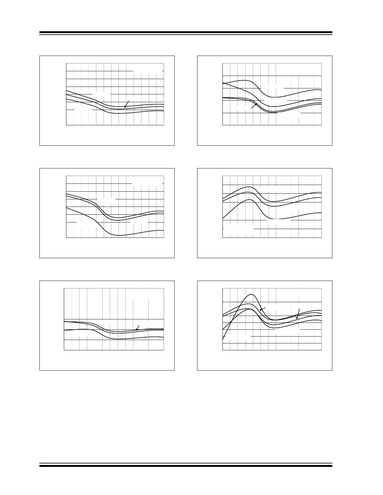
FIGURE 2-19:
Load Regulation vs.
Temperature (V
R
= 1.8V).
FIGURE 2-20:
Load Regulation vs.
Temperature (V
R
= 3.0V).
FIGURE 2-21:
Load Regulation vs.
Temperature (V
R
= 5.0V).
FIGURE 2-22:
Line Regulation vs.
Temperature (V
R
= 1.8V).
FIGURE 2-23:
Line Regulation vs.
Temperature (V
R
= 3.0V).
FIGURE 2-24:
Line Regulation vs.
Temperature (V
R
= 5.0V).
-0.40
-0.35
-0.30
-0.25
-0.20
-0.15
-0.10
-0.05
0.00
-40 -30 -20 -10
0
10
20
30
40
50
60
70
80
90
Temperature (°C)
Load R
e
gul
ati
on (%
)
V
R
= 1.8V
I
OUT
= 1 to 30mA
V
IN
= 6.0V
V
IN
= 2.8V
V
IN
= 4.0V
-0.70
-0.65
-0.60
-0.55
-0.50
-0.45
-0.40
-0.35
-0.30
-40 -30 -20 -10
0
10
20
30
40
50
60
70
80
90
Temperature (°C)
Load R
e
gul
ati
on (%
)
V
IN
= 10.0V
V
IN
= 4.0V
V
IN
= 6.0V
V
R
= 3.0V
I
OUT
= 1 to 80 mA
-0.6
-0.5
-0.4
-0.3
-0.2
-0.1
0.0
-40 -30 -20 -10
0
10
20
30
40
50
60
70
80
90
Temperature (°C)
Load R
e
gul
ati
on (%
)
V
IN
= 10.0V
V
IN
= 7.0V
V
IN
= 6.0V
V
R
= 5.0V
I
OUT
= 1 to 100 mA
0.10
0.11
0.12
0.13
0.14
0.15
-40 -30 -20 -10
0
10
20
30
40
50
60
70
80
90
Temperature (°C)
Li
ne R
e
gul
ati
on (%
/V
)
I
OUT
= 10 mA
I
OUT
= 1 mA
I
OUT
= 90 mA
I
OUT
= 40 mA
V
R
= 1.8V
V
IN
= 2.8V to 10V
0.06
0.07
0.08
0.09
0.10
0.11
0.12
0.13
-40 -30 -20 -10
0
10
20
30
40
50
60
70
80
90
Temperature (°C)
Li
ne R
e
gul
ati
on (%
/V
)
I
OUT
= 10 mA
I
OUT
= 150 mA
I
OUT
= 1 mA
V
R
= 3.0V
V
IN
= 4.0V to 10V
0.08
0.09
0.10
0.11
0.12
0.13
0.14
0.15
0.16
0.17
-40 -30 -20 -10
0
10
20
30
40
50
60
70
80
90
Temperature (°C)
Li
ne R
e
gul
ati
on (%
/V
)
V
R
= 5.0V
V
IN
= 6.0V to 10V
I
OUT
= 100 mA
I
OUT
= 250 mA
I
OUT
= 1 mA
I
OUT
= 10 mA
©
2005 Microchip Technology Inc.
DS21874B-page 9
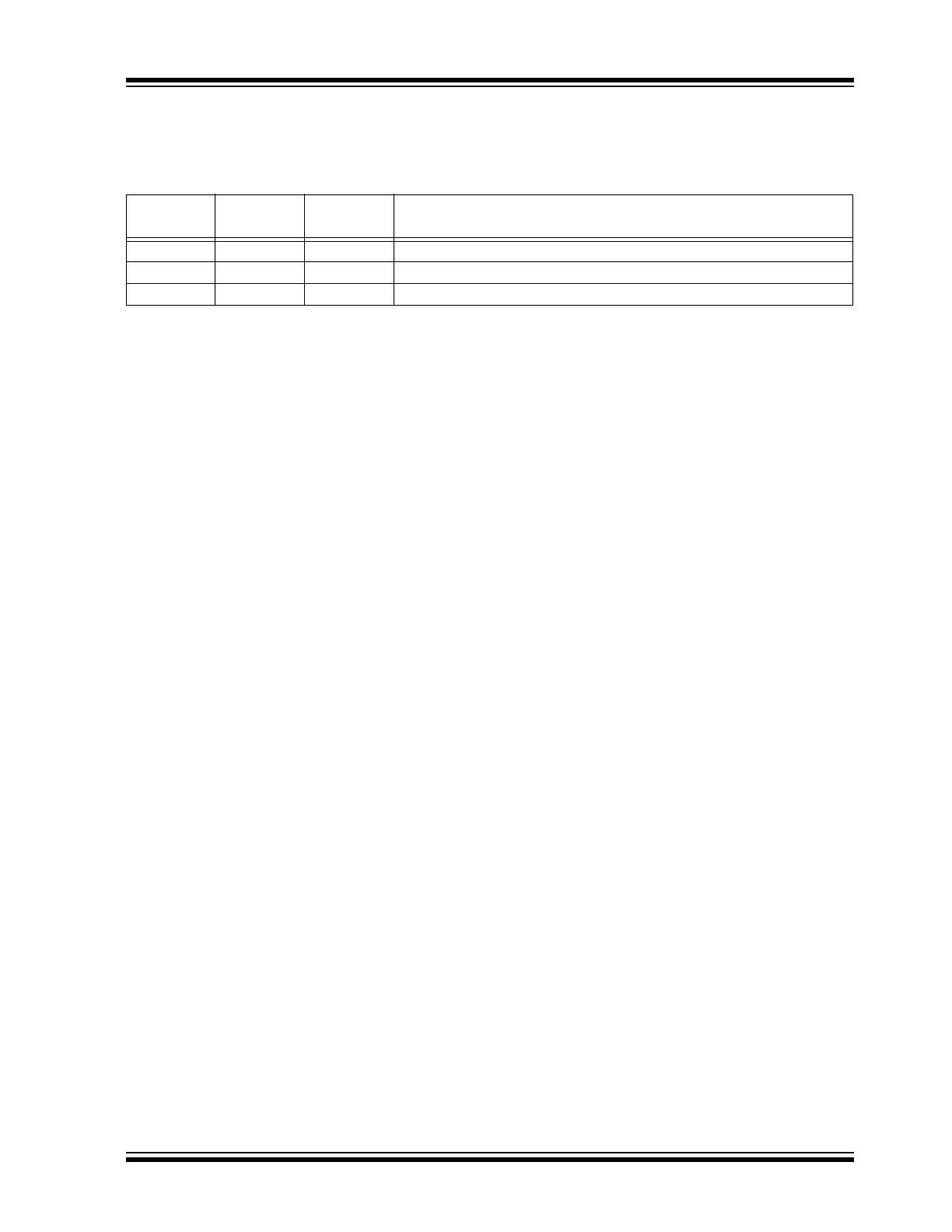
MCP1701
3.0
PIN DESCRIPTIONS
The descriptions of the pins are listed in Table 3-1.
TABLE 3-1:
PIN FUNCTION TABLE
3.1
Ground Terminal (GND)
Regulator ground. Tie GND to the negative side of the
output and the negative side of the input capacitor.
Only the LDO bias current (2 µA, typ.) flows out of this
pin, there is no high current. The LDO output regulation
is referenced to this pin. Minimize voltage drops
between this pin and the negative side of the load.
3.2
Regulated Voltage Output (V
OUT
)
Connect V
OUT
to the positive side of the load and the
positive terminal of the output capacitor. The positive
side of the output capacitor should be physically
located as close as possible to the LDO V
OUT
pin. The
current flowing out of this pin is equal to the DC load
current.
3.3
Unregulated Supply Input (V
IN
)
Connect the input supply voltage and the positive side
of the input capacitor to V
IN
. Like all low dropout linear
regulators, low source impedance is necessary for the
stable operation of the LDO. The amount of
capacitance required to ensure low source impedance
will depend on the proximity of the input source
capacitors or battery type. The input capacitor should
be physically located as close as possible to the V
IN
pin. For most applications, 1 µF of capacitance will
ensure stable operation of the LDO circuit. For applica-
tions that have load currents below 100 mA, the input
capacitance requirement can be lowered. The type of
capacitor used can be ceramic, tantalum or aluminum
electrolytic. The low equivalent series resistence
characteristics of the ceramic will yield better noise and
PSRR performance at high frequency. The current flow
into this pin is equal to the DC load current, plus the
LDO bias current (2 µA, typ.).
Pin No.
SOT-23A
Pin No.
SOT-89
Name
Function
1
1
GND
Ground Terminal
2
3
V
OUT
Regulated Voltage Output
3
2
V
IN
Unregulated Supply Input
MCP1701
DS21874B-page 10
©
2005 Microchip Technology Inc.
4.0
DETAILED DESCRIPTION
The MCP1701 is a low quiescent current, precision,
fixed-output voltage LDO. Unlike bipolar regulators,
the MCP1701 supply current does not increase
proportionally with load current.
4.1
Output Capacitor
A minimum of 1 µF output capacitor is required. The
output capacitor should have an ESR greater than
0.1
Ω
and less than 5
Ω
, plus a resonant frequency
above 1 MHz. Larger output capacitors can be used to
improve supply noise rejection and transient response.
Care should be taken when increasing C
OUT
to ensure
that the input impedance is not high enough to cause
high input impedance oscillation.
4.2
Input Capacitor
A 1 µF input capacitor is recommended for most
applications when the input impedance is on the order
of 10
Ω
. Larger input capacitance may be required for
stability when operating from a battery input, or if there
is a large distance from the input source to the LDO.
When large values of output capacitance are used, the
input capacitance should be increased to prevent high
source impedance oscillations.
4.3
Overcurrent
The MCP1701 internal circuitry monitors the amount of
current flowing through the P-channel pass transistor.
In the event of a short circuit or excessive output
current, the MCP1701 will act to limit the output current.
FIGURE 4-1:
Block Diagram.
V
IN
V
OUT
GND
Short Circuit
Protection
Voltage
Reference
+
–