

© 2008 Microchip Technology Inc.
DS22083A-page 1
MCP14628
Features
• Dual Output MOSFET Driver for Synchronous
Applications
• High Peak Output Current: 2A (typical)
• Adaptive Cross Conduction Protection
• Internal Bootstrap Blocking Device
• +36V BOOT Pin Maximum Rating
• Enhanced Light Load Efficiency Mode
• Low Supply Current: 80 µA (typical)
• High Capacitive Load Drive Capability:
- 3300 pF in 10 ns (typical)
• Tri-State PWM Pin for Power Stage Shutdown
• Input Voltage Undervoltage Lockout Protection
• Space Saving Packages:
- 8-Lead SOIC
- 8-Lead 3x3 DFN
Applications
• High Efficient Synchronous DC/DC Buck
Converters
• High Current Low Output Voltage Synchronous
DC/DC Buck Converters
• High Input Voltage Synchronous DC/DC Buck
Converters
• Core Voltage Supplies for Microprocessors
General Description
The MCP14628 is a dual MOSFET gate driver
designed to optimally drive two N-Channel MOSFETs
arranged in a non-isolated synchronous buck converter
topology. With the capability to source 2A peaks
typically from both the high-side and low-side drives,
the MCP14628 is an ideal companion to buck control-
lers that lack integrated gate drivers. Additionally,
greater design flexibility is offered by allowing the gate
drivers to be placed close to the power MOSFETs.
The MCP14628 features the capability to sink 3.5A
peak typically for the low-side gate drive. This allows
the MCP14628 the capability of holding off the low-side
power MOSFET during the rising edge of the PHASE
node. Internal adaptive cross conduction protection
circuitry is also used to mitigate both external power
MOSFETs from simultaneously conducting.
The low resistance pull-up and pull-down drives allow
the MCP14628 to quickly transition a 3300 pF load in
typically 10 ns and with a propagation time of typically
20 ns. Bootstrapping for the high-side drive is internally
implemented which allows for a reduced system cost
and design complexity.
The PWM input to the MCP14628 can be tri-stated to
force both drive outputs low for true power stage
shutdown. Light load system efficiency is improved by
using the diode emulation feature of the MCP14628.
When the FCCM pin is grounded, diode emulation
mode is entered. In this mode, discontinuous conduc-
tion is allowed by sensing when the inductor current
reach zero and turning off the low-side power
MOSFET.
Package Types
1
2
3
4
8
7
6
5
HIGHDR
BOOT
PWM
GND
LOWDR
V
CC
FCCM
PHASE
8-Lead SOIC
1
2
3
4
8
7
6
5
HIGHDR
BOOT
PWM
GND
LOWDR
V
CC
FCCM
PHASE
8-Lead DFN
Note 1: Exposed pad on the DFN is electrically isolated.
2A Synchronous Buck Power MOSFET Driver
MCP14628
DS22083A-page 2
© 2008 Microchip Technology Inc.
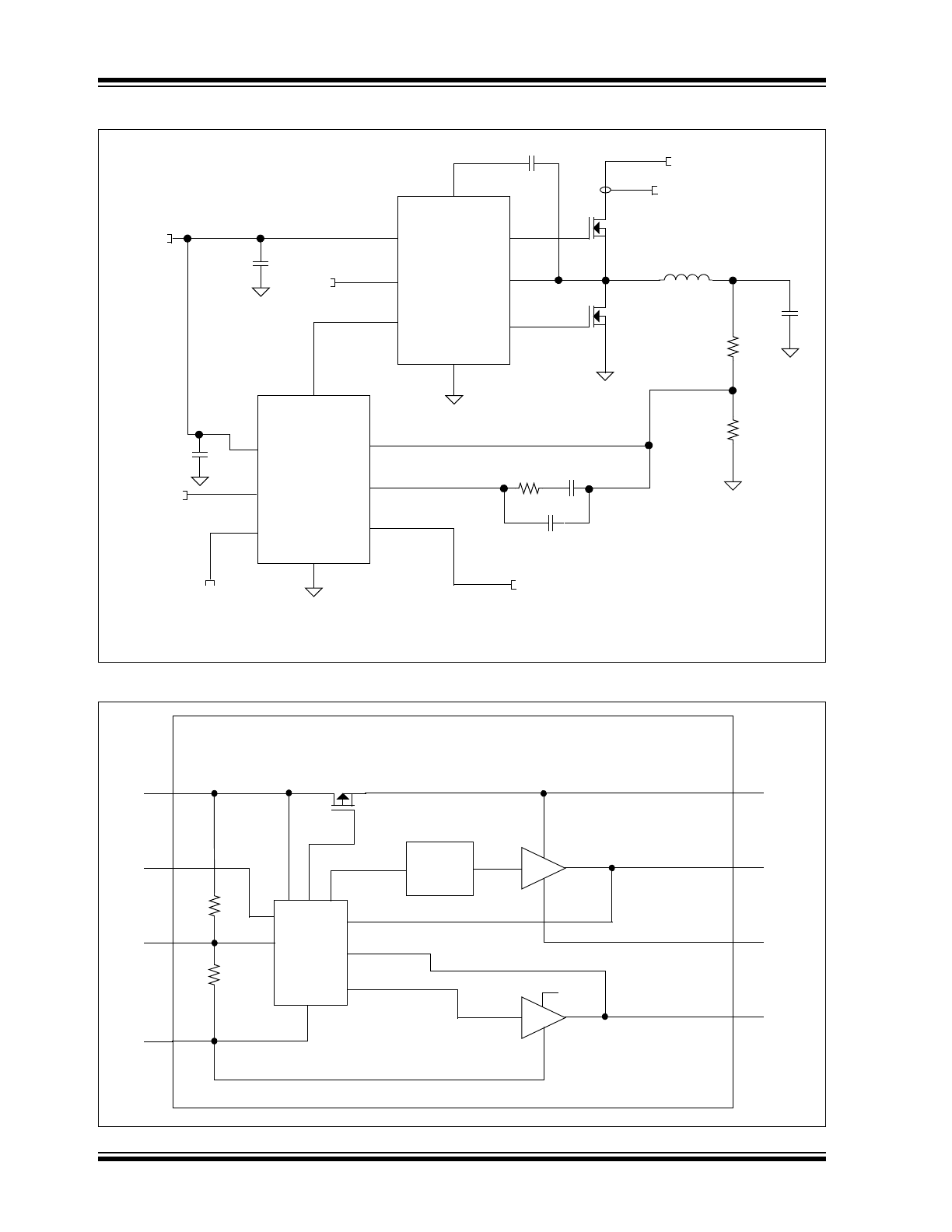
Typical Application Schematic
Functional Block Diagram
UGATE
LGATE
PHASE
GND
BOOT
V
CC
FCCM
PWM
C
BOOT
FB
V
REF
COMP
GND
VEXT
V
CC
CS
OSC IN
MCP1630
MCP14628
REFERENCE VOLTAGE
V
SUPPLY
= 12V
V
CC
= 5V
OSCILLATOR
FROM MCU
CURRENT
SENSE
CURRENT
SENSE
Q
H
Q
L
FCCM
CONTROL
BOOT
HIGHDR
PHASE
LOWDR
V
CC
FCCM
PWM
GND
V
CC
R
R
Level
Shift
Control
Logic &
Protection
© 2008 Microchip Technology Inc.
DS22083A-page 3
MCP14628
1.0
ELECTRICAL
CHARACTERISTICS
Absolute Maximum Ratings †
V
CC
, Device Supply Voltage............................. -0.3V to +7.0V
V
BOOT
, BOOT Voltage.................................... -0.3V to +36.0V
V
PHASE
, Phase Voltage........... V
BOOT
- 7.0V to V
BOOT
+ 0.3V
V
FCCM
, FCCM Voltage ........................... -0.3V to V
CC
+ .0.3V
V
PWM
, PWM Voltage ............................... -0.3V to V
CC
+ 0.3V
V
UGATE
, UGATE Voltage ....... V
PHASE
- 0.3V to V
BOOT
+ 0.3V
V
LGATE
, LGATE Voltage .......................... -0.3V to V
CC
+ 0.3V
ESD Protection on all Pins ....................................2 kV (HBM)
† Notice: Stresses above those listed under "Maximum
Ratings" may cause permanent damage to the device. This is
a stress rating only and functional operation of the device at
those or any other conditions above those indicated in the
operational sections of this specification is not intended.
Exposure to maximum rating conditions for extended periods
may affect device reliability.
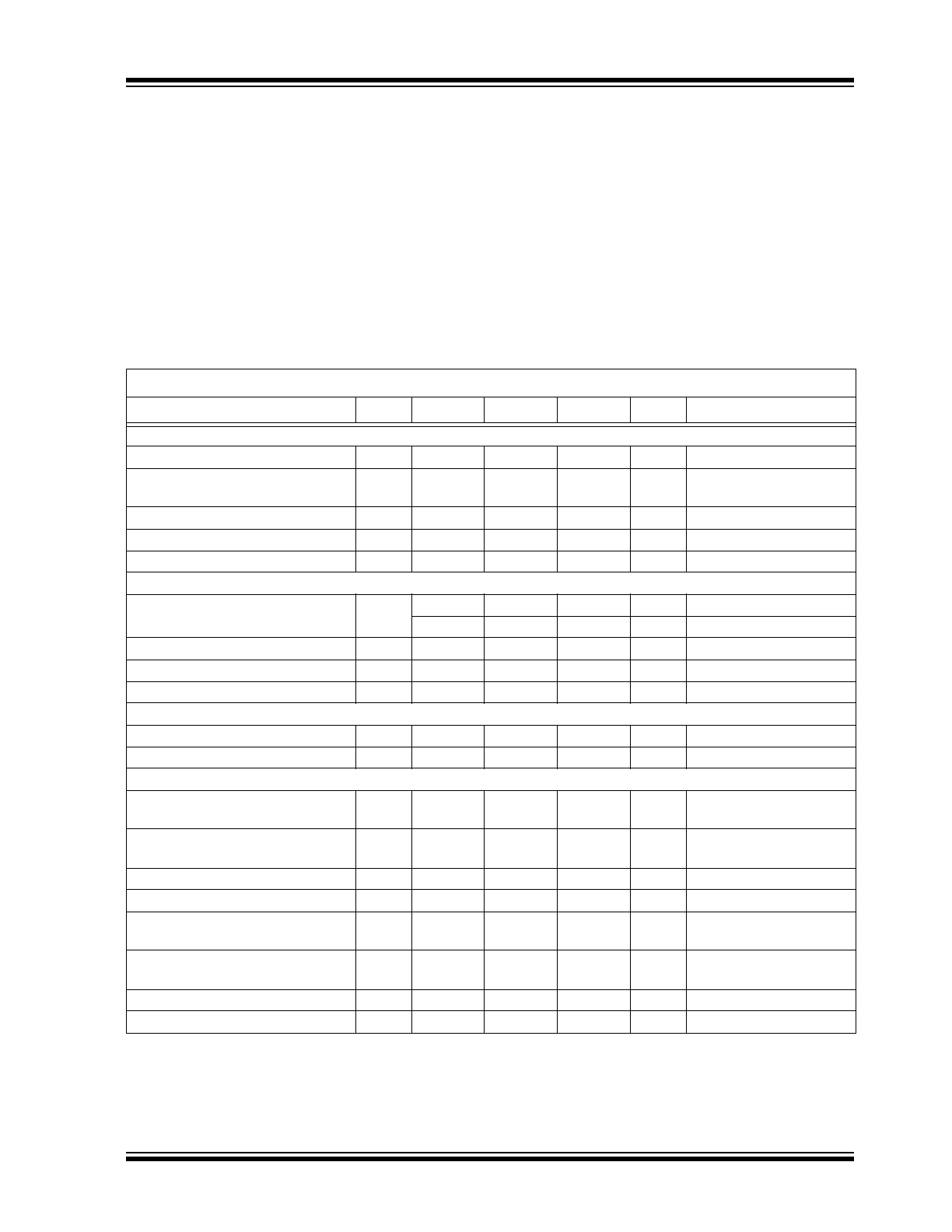
DC CHARACTERISTICS
Electrical Specifications: Unless otherwise noted, V
CC
= 5V, T
J
= -40°C to +125°C
Parameters
Sym
Min
Typ
Max
Units
Conditions
V
CC
Supply Requirements
Recommended Operating Range
V
CC
4.5
5.0
5.5
V
Bias Supply Voltage
I
VCC
—
80
—
µA
PWM pin floating,
V
FCCM
= 5V
UVLO (Rising V
CC
)
—
3.40
3.90
V
UVLO (Falling V
CC
)
2.40
2.90
—
V
Hysteresis
—
500
—
mV
PWM Input Requirements
PWM Input Current
I
PWM
—
250
—
µA
V
PWM
= 5V
—
-250
—
µA
V
PWM
= 0V
PWM Rising Threshold
0.70
1.00
1.30
V
PWM Falling Threshold
3.50
3.80
4.10
V
Tri-State Shutdown Hold-off Time
t
TSSHD
100
175
250
ns
T
A
= +25°C, Note 2
FCCM input Requirements
FCCM Low Threshold
0.50
—
—
V
FCCM High Threshold
—
—
2.0
V
Output Requirements
High Drive Source Resistance
—
1.0
2.5
Ω
500 mA source current,
Note 1
High Drive Sink Resistance
—
1.0
2.5
Ω
500 mA sink current,
Note 1
High Drive Source Current
—
2.0
—
A
Note 1
High Drive Sink Current
—
2.0
—
A
Note 1
Low Drive Source Resistance
—
1
2.5
Ω
500 mA source current,
Note 1
Low Drive Sink Resistance
—
0.5
1.0
Ω
500 mA sink current,
Note 1
Low Drive Source Current
—
2.0
—
A
Note 1
Low Drive Sink Current
—
3.5
—
A
Note 1
Note 1:
Parameter ensured by design, not production tested.
2:
See
Figure 4-1
for parameter definition.
MCP14628
DS22083A-page 4
© 2008 Microchip Technology Inc.
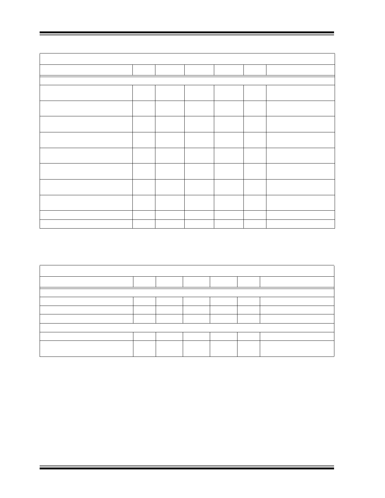
TEMPERATURE CHARACTERISTICS
Switching Times
HIGHDR Rise Time
t
RH
—
10
—
ns
C
L
= 3.3nF,
Note 1, Note 2
LOWDR Rise Time
t
RL
—
10
—
ns
C
L
= 3.3nF,
Note 1, Note 2
HIGHDR Fall Time
t
FH
—
10
—
ns
C
L
= 3.3nF,
Note 1, Note 2
LOWDR Fall Time
t
FL
—
6.0
—
ns
C
L
= 3.3nF,
Note 1, Note 2
HIGHDR Turn-off Propagation
Delay
t
PDLH
—
15
—
ns
No Load, Note 2
LOWDR Turn-off Propagation
Delay
t
PDLL
—
16
—
ns
No Load, Note 2
HIGHDR Turn-on Propagation
Delay
t
PDHH
10
18
30
ns
No Load, Note 2
LOWDR Turn-on Propagation
Delay
t
PDHL
10
22
30
ns
No Load, Note 2
Tri-State Propagation Delay
t
PTS
—
35
—
ns
No Load, Note 2
Minimum LOWDR On Time in DCM
t
LGMIN
—
400
—
ns
FCCM pin low Note 1
Electrical Specifications: Unless otherwise noted, all parameters apply with V
CC
= 5V.
Parameter
Sym
Min
Typ
Max
Units
Comments
Temperature Ranges
Specified Temperature Range
T
A
-40
—
+85
°C
Maximum Junction Temperature
T
J
—
—
+150
°C
Storage Temperature
T
A
-65
—
+150
°C
Package Thermal Resistances
Thermal Resistance, 8L-SOIC
θ
JA
—
149.5
—
°C/W
Thermal Resistance, 8L-DFN (3x3)
θ
JA
—
60.0
—
°C/W
Typical Four-layer board
with vias to ground plane
DC CHARACTERISTICS (CONTINUED)
Electrical Specifications: Unless otherwise noted, V
CC
= 5V, T
J
= -40°C to +125°C
Parameters
Sym
Min
Typ
Max
Units
Conditions
Note 1:
Parameter ensured by design, not production tested.
2:
See
Figure 4-1
for parameter definition.
© 2008 Microchip Technology Inc.
DS22083A-page 5
MCP14628
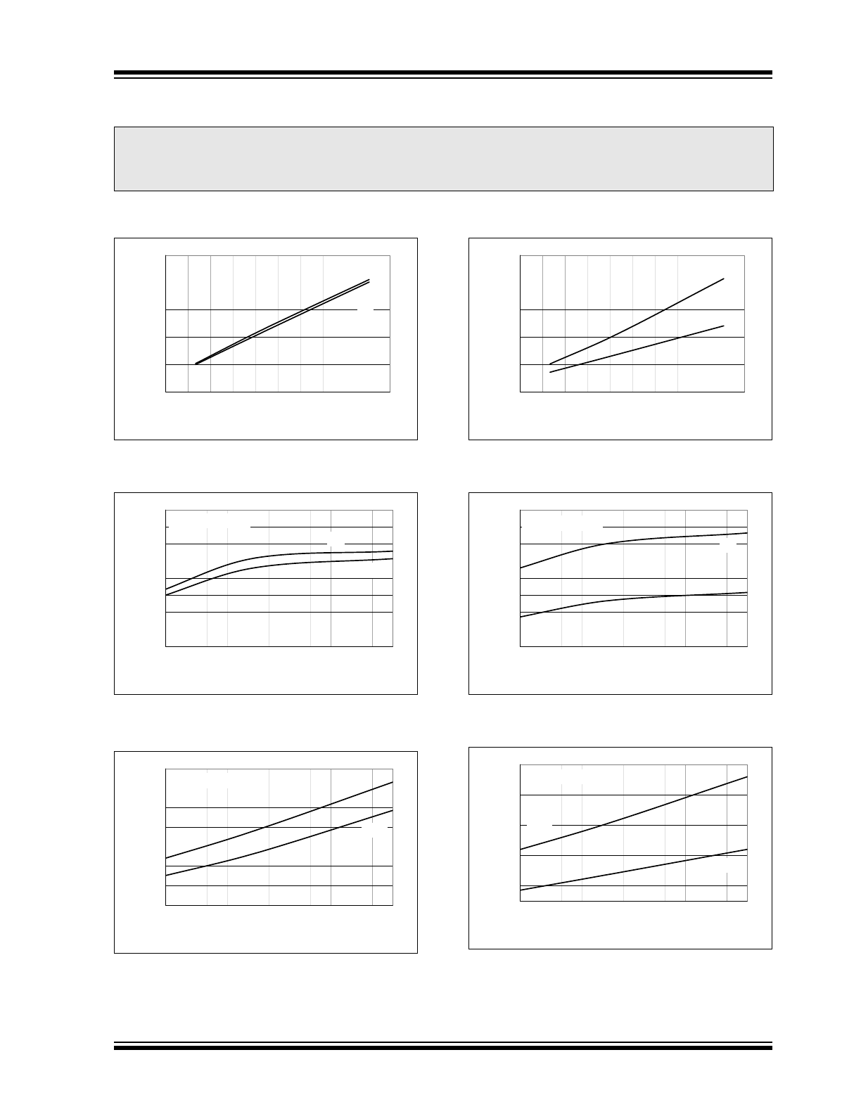
2.0
TYPICAL PERFORMANCE CURVES
Note: Unless otherwise indicated, T
A
= +25°C with V
CC
= 5.0V.
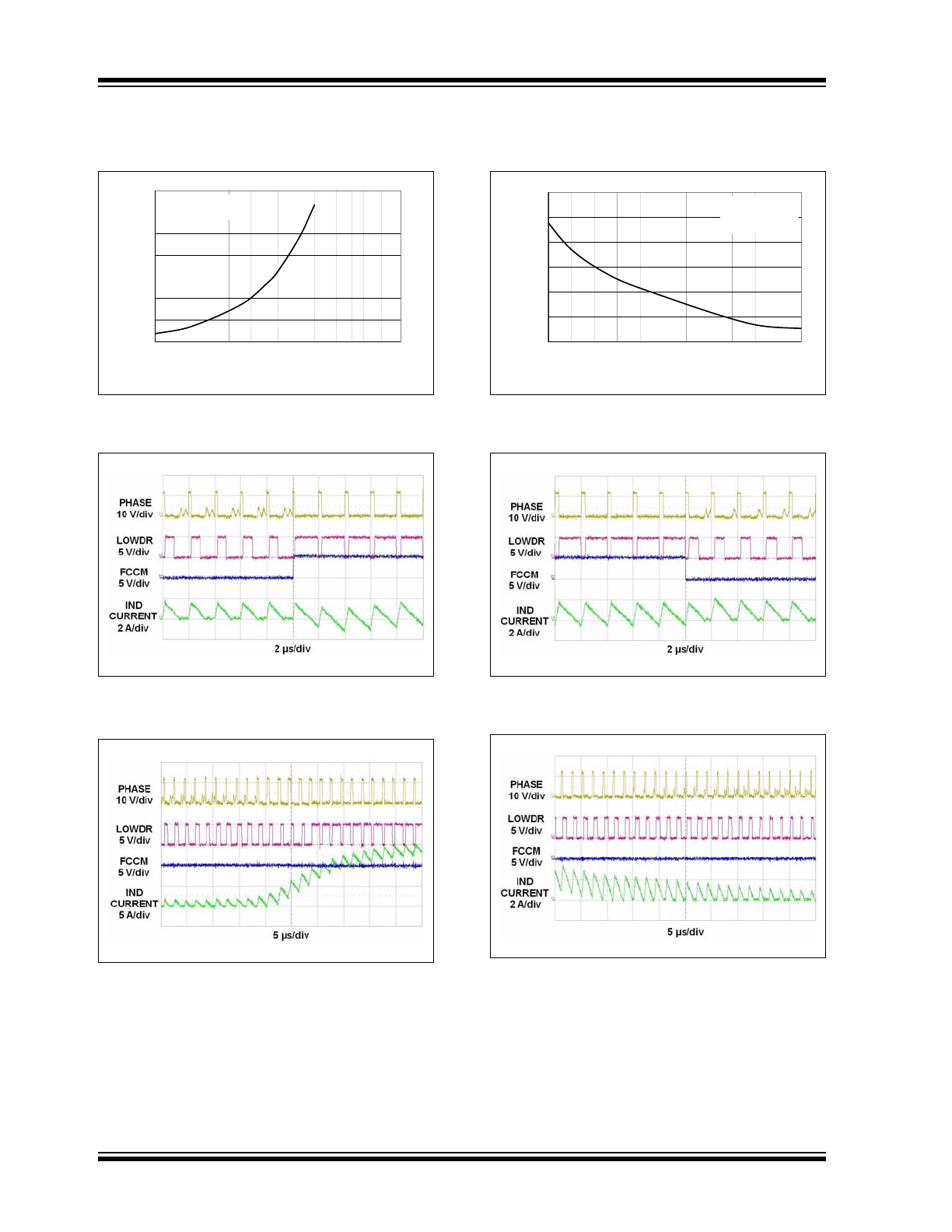
FIGURE 2-1:
Rise Times vs. Capacitive
Load.
FIGURE 2-2:
HIGHDR Rise and Fall Time
vs. Temperature.
FIGURE 2-3:
HIGHDR Propagation Delay
vs. Temperature.
FIGURE 2-4:
Fall Times vs. Capacitive
Load.
FIGURE 2-5:
LOWDR Rise and Fall Time
vs. Temperature.
FIGURE 2-6:
LOWDR Propagation Delay
vs. Temperature.
Note:
The graphs and tables provided following this note are a statistical summary based on a limited number of
samples and are provided for informational purposes only. The performance characteristics listed herein are
not tested or guaranteed. In some graphs or tables, the data presented may be outside the specified
operating range (e.g., outside specified power supply range) and therefore outside the warranted range.
0
5
10
15
20
25
0
1500
3000
4500
6000
7500
Capacitive Load (pF)
Ri
se Ti
m
e
(ns
)
t
RH
t
RL
6
7
8
9
10
11
12
13
14
-40 -25 -10
5
20
35
50
65
80
95 110 125
Temperature (°C)
Time (
n
s)
t
RH
t
FH
C
LOAD
= 3,300 pF
10
12
14
16
18
20
22
24
-40 -25 -10
5
20
35
50
65
80
95 110 125
Temperature (°C)
P
ropagation Delay (ns)
t
PDHH
t
PDLH
C
LOAD
= 3,300 pF
0
5
10
15
20
25
0
1500
3000
4500
6000
7500
Capacitive Load (pF)
Fall Time (ns)
t
FH
t
FL
4
5
6
7
8
9
10
11
12
-40 -25 -10
5
20
35
50
65
80
95 110 125
Temperature (°C)
Time (
n
s)
t
RL
t
FL
C
LOAD
= 3,300 pF
12
14
16
18
20
22
24
26
28
30
-40 -25 -10
5
20
35
50
65
80
95 110 125
Temperature (°C)
Time (
n
s)
t
PDHL
t
PDLL
C
LOAD
= 3,300 pF
MCP14628
DS22083A-page 6
© 2008 Microchip Technology Inc.
Typical Performance Curves (Continued)
Note: Unless otherwise indicated, T
A
= +25°C with V
CC
= 5.0V.
FIGURE 2-7:
Supply Current vs.
Frequency.
FIGURE 2-8:
DCM to CCM Transition
Operation.
FIGURE 2-9:
Load Transition
(0.5A - 15A).
FIGURE 2-10:
Supply Current vs.
Temperature.
FIGURE 2-11:
CCM to DCM Transition
Operation.
FIGURE 2-12:
Load Transition
(15A - 0.5A).
0
10
20
30
40
50
60
70
100
1000
10000
Frequency (kHz)
S
upply Current
(mA)
C
LOAD
= 3,300 pF
Duty Cycle = 30%
580
600
620
640
660
680
700
-40 -25 -10
5
20
35
50
65
80
95
110 125
Temperature (°C)
Supp
ly Curre
nt
(
µ
A)
C
LOAD
= 3,300 pF
F
SW
= 12.5 kHz
Duty Cycle = 30%
© 2008 Microchip Technology Inc.
DS22083A-page 7
MCP14628
Typical Performance Curves (Continued)
Note: Unless otherwise indicated, T
A
= +25°C with V
CC
= 5.0V.
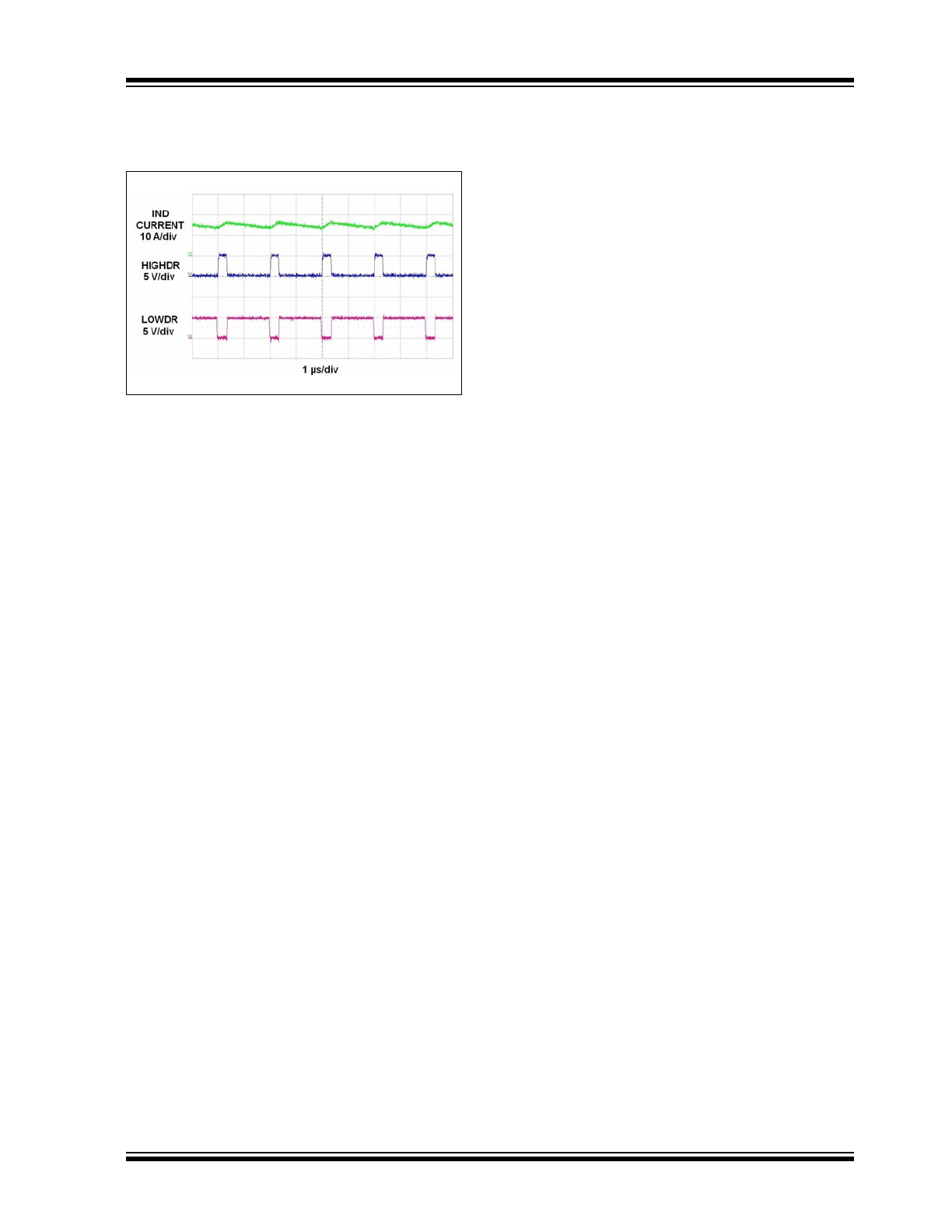
FIGURE 2-13:
HIGHDR and LOWDR
Operation.

MCP14628
DS22083A-page 8
© 2008 Microchip Technology Inc.
3.0
PIN DESCRIPTIONS
The descriptions of the pins are listed in
Table 3-1
.
TABLE 3-1:
PIN FUNCTION TABLE .
3.1
High-side Gate Driver Pin
(HIGHDR)
The HIGHDR pin provides the gate drive signal to
control the high-side power MOSFET. The gate of the
high-side power MOSFET is connected to this pin.
3.2
Floating Bootstrap Supply Pin
(BOOT)
The BOOT pin is the floating bootstrap supply pin for
the high-side gate drive. A capacitor is connected
between this pin and the PHASE pin to provide the
necessary charge to turn on the high-side power MOS-
FET.
3.3
PWM Input Control Pin (PWM)
The control input signal is supplied to the PWM pin.
This tri-state pin controls the state of the HIGHDR and
LOWDR pins. Placing a voltage equal to V
CC
/2 on this
pin causes both the HIGHDR and LOWDR to a low
state.
3.4
Ground Pin (GND)
The GND pin provides ground for the MCP14628 cir-
cuitry. It should have a low impedance connection to
the bias supply source return. High peak currents will
flow out the GND pin when the low-side power
MOSFET is being turned off.
3.5
Low-side Gate Driver Pin
(LOWDR)
The LOWDR pin provides the gate drive signal to
control the low-side power MOSFET. The gate of the
low-side power MOSFET is connected to this pin.
3.6
Supply Input Voltage Pin (V
CC
)
The V
CC
pin provides bias to the MCP14628. A bypass
capacitor is to be placed between this pin and the GND
pin. This capacitor should be placed as close to the
MCP14628 as possible.
3.7
Forced Continuous Conduction
Mode Pin (FCCM)
The FCCM pin enables or disables the forced
continuous conduction mode. With the FCCM pin con-
nected to ground the MCP14628 enters a diode emula-
tion mode to improve system efficiency at light loads.
Continuous conduction is forced if the FCCM pin is
connected to V
CC
.
3.8
Switch Node Pin (PHASE)
The PHASE pin provides the return path for the high-
side gate driver. The source of the high-side power
MOSFET is connected to this pin.
3.9
DFN Exposed Pad
The exposed metal pad of the DFN package is not
internally connected to any potential. Therefore, this
pad can be connected to a ground plane or other
copper plane on a printed circuit board to aid in heat
removal from the package.
SOIC
3x3 DFN
Symbol
Description
1
1
HIGHDR
High-side Gate Driver Pin
2
2
BOOT
Floating Bootstrap Supply Pin
3
3
PWM
PWM Input Control Pin
4
4
GND
Ground
5
5
LOWDR
Low-side Gate Driver Pin
6
6
V
CC
Supply Input Voltage
7
7
FCCM
Forced Continuous Conduction Mode Pin
8
8
PHASE
Switch Node Pin
—
PAD
NC
Exposed Metal Pad

© 2008 Microchip Technology Inc.
DS22083A-page 9
MCP14628
4.0
DETAILED DESCRIPTION
4.1
Device Overview
The MCP14628 is a dual MOSFET gate driver
designed to optimally drive both high-side and low-side
N-channel MOSFETs arranged in a non-isolated
synchronous buck converter topology.
The MCP14628 is capable of suppling 2A (typical)
peak current to the floating high-side power MOSFET
that is connected to the HIGHDR pin. With the excep-
tion of a capacitor, all of the circuitry needed to drive
this high-side N-channel MOSFET is internal to the
MCP14628. A blocking device is placed between the
V
CC
and BOOT pins that allows the bootstrap capacitor
to be charged to V
CC
when the low-side power MOS-
FET is conducting. Refer to Section 5.1, for informa-
tion on determining the proper size of the bootstrap
capacitor. The HIGHDR is also capable of sinking 2A
(typical) peak current.
The LOWDR is capable of sourcing 2A (typical) peak
current and sinking 3.5A (typical) peak current. This
helps ensure that the low-side power MOSFET stays
turned off during the high dv/dt of the PHASE node.
4.2
Adaptive Cross-Conduction
Protection
The MCP14628 prevents cross-conduction power loss
by adaptively ensuring that the high-side and low-side
power MOSFETs are not conducting simultaneously.
When the PWM signal goes low, the HIGHDR is pulled
low and the LOWDR signal is held low until the
HIGHDR reach 1V (typically). At that time, the LOWDR
is allowed to turn on.
4.3
FCCM Mode
The MCP14628 features a diode emulation mode to
enhance the light load system efficiency. The FCCM
pin enables or disables the diode emulating mode. With
the FCCM pin grounded, diode emulation mode is
entered. The forced continuous conduction mode is
entered when the FCCM pin is connected to V
CC
.
In diode emulation mode, the MCP14628 turns off the
low-side power MOSFET when the inductor current
reaches approximately zero even if the PWM input sig-
nal is still low. The LOWDR and HIGHDR both stay low
until the next switching cycle begins. To prevent false
termination of the LOWDR signal, there is a 400 ns
minimum on time, t
LGMIN
, of the LOWDR. This also
ensures that the bootstrap capacitor is fully charged.
In forced continuous conduction mode, the LOWDR of
the MCP14628 does not terminate until the PWM input
signal transitions from a low to a high.
4.4
Tri-State PWM
The PWM input pin of the MCP14628 controls the high
current LOWDR and HIGHDR drive signals. These
signals have three distinct operating modes depending
upon the state of the PWM input signal.
A logic low on the PWM pin cause the LOWDR drive
signal to be high and the HIGHDR drive signal to be
low. When the PWM signal transitions to a logic high,
the LOWDR signal goes low and the HIGHDR signal go
high. To ensure proper operation the PWM input signal
should be capable of a logic low of 0V and a logic high
of 5V.
The third operating mode of the drive signals occurs
when the PWM signal is set to a value equal to V
CC
/2
(typically). When the PWM signal dwells at this voltage
for 175 ns (typically) the MCP14628 disables both
LOWDR and HIGHDR drive signals. Both drive signals
are pulled and held low. Once the PWM signal moves
beyond V
CC
/2, the MCP14628 removes the shutdown
state of the drive signals.
MCP14628
DS22083A-page 10
© 2008 Microchip Technology Inc.
4.5
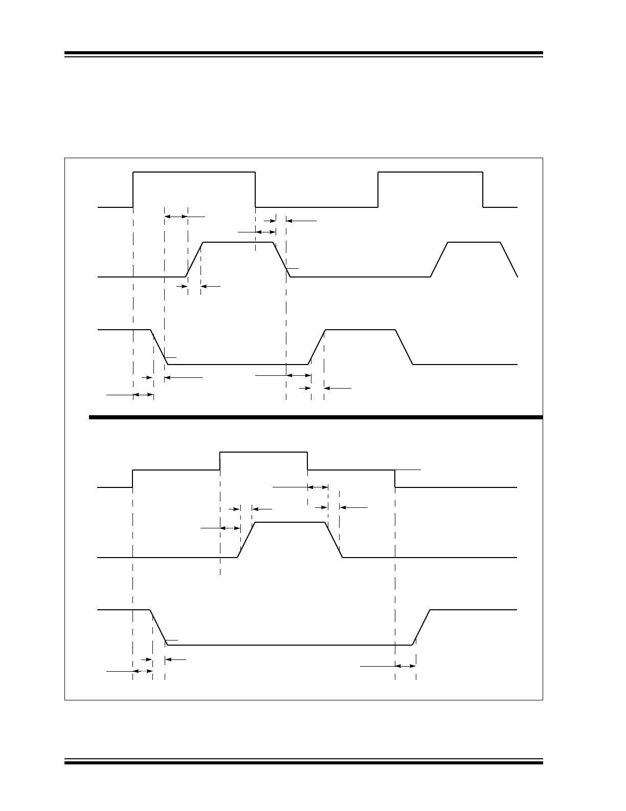
Timing Diagram
The PWM signal applied to the MCP14628 is suppled
by a controller IC that regulates the power supply
output. The timing diagram in
Figure 4-1
graphically
depicts the PWM signal and the output signals of the
MCP14628.
FIGURE 4-1:
MCP14628 Timing Diagram.
PWM
HIGHDR
LOWDR
t
PDLL
t
FL
t
PDHH
t
RH
t
PDLH
t
FH
t
RL
t
PDHL
1V
1
V
PWM
HIGHDR
LOWDR
V
CC
/2
t
PTS
t
TSSHD
t
RH
t
PTS
t
FH
t
FL
t
TSSHD
1V
V
CC
0V
V
CC