
2017 Microchip Technology Inc.
DS20005603A-page 1
MIC45208-1/-2
Features
• No Compensation Required
• Up to 10A Output Current
• >93% Peak Efficiency
• Output Voltage: 0.8V to 0.85*V
IN
with
±1% Accuracy
• Adjustable Switching Frequency from 200 kHz to
600 kHz
• Enable Input and Open-Drain Power Good (PG)
Output
• Hyper Speed Control
®
(MIC45208-2) Architecture
enables Fast Transient Response
• HyperLight Load
®
(MIC45208-1) improves Light
Load Efficiency
• Supports Safe Start-up into Pre-Biased Output
• –40 C to +125°C Junction Temperature Range
• Thermal Shutdown Protection
• Short-Circuit Protection with Hiccup mode
• Adjustable Current Limit
• Available in 52-Pin 10 mm x 10 mm x 4 mm QFN
Package
Applications
• High-Power Density Point-of-Load (POL)
Conversion
• Servers, Routers, Networking and Base Stations
• FPGAs, DSP and Low-Voltage ASIC Power Supplies
• Industrial and Medical Equipment
General Description
The MIC45208-1/-2 is a synchronous, step-down regula-
tor module, featuring a unique adaptive ON-time control
architecture. The module incorporates a DC-to-DC
controller, power MOSFETs, bootstrap diode, bootstrap
capacitor and an inductor in a single package, simplifying
the design and layout process for the end user.
This highly integrated solution expedites system
design and improves product time-to-market. The
internal MOSFETs and inductor are optimized to
achieve high efficiency at a low-output voltage. The
fully optimized design can deliver up to 10A current
under a wide input voltage range of 4.5V to 26V,
without requiring additional cooling.
The MIC45208-1 uses the HyperLight Load (HLL) while
the MIC45208-2 uses Hyper Speed Control (HSC) archi-
tecture, which enables ultra-fast load transient
response, allowing for a reduction of output capacitance.
The MIC45208 offers 1% output accuracy that can be
adjusted from 0.8V to 0.85*V
IN
with two external
resistors. Additional features include thermal shutdown
protection, input undervoltage lockout, adjustable
current limit and short-circuit protection. The MIC45208
allows for safe start-up into a pre-biased output.
Data sheet and other support documentation can be
found on the Microchip web site at:
www.microchip.com
.
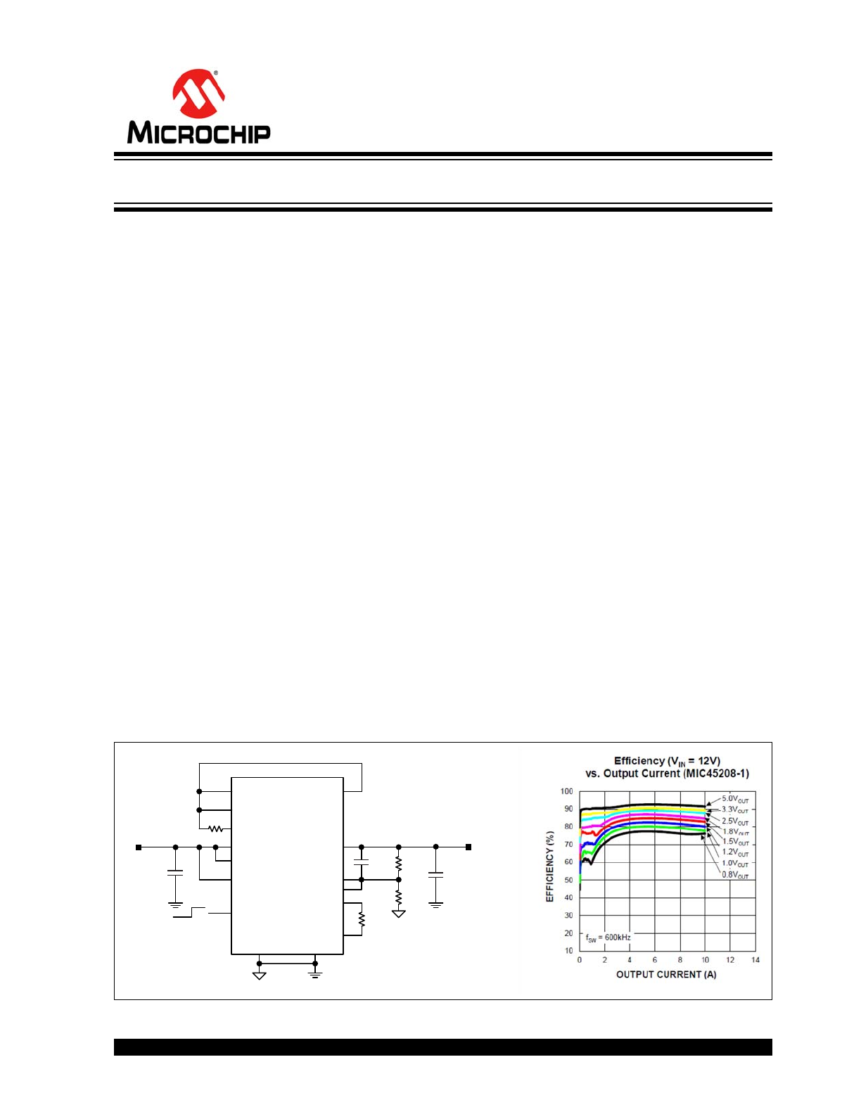
Typical Application Schematic
R
FB1
V
OUT
1.5V/10A
MIC45208
V
IN
12V
C
OUT
C
IN
GND
PV
IN
V
OUT
R
FB2
FB
SW
I
LIM
PGND
BST
ANODE
EN
FREQ
ON
PG
PV
DD
5V
DD
R
LIM
RIB
OFF
V
IN
C
FF
RIA
26V, 10A DC-to-DC Power Module
MIC45208-1/-2
DS20005603A-page 2
2017 Microchip Technology Inc.
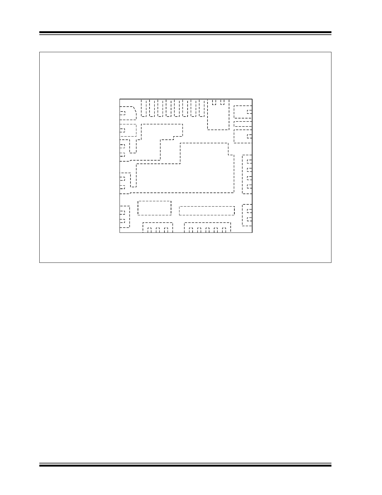
Package Types
5V
DD
5V
DD
PV
DD
PV
IN
PV
DD
PGND
PGND
PGND
KEEPOUT
SW
SW
SW
KEEPOUT
PV
IN
PV
IN
ANODE
ANODE
RIB
V
OUT
RIA
RIA
KEEPOUT
SW
SW
SW
SW
SW
KEEPOUT
V
OUT
V
OUT
GND
I
LIM
FREQ
V
IN
EN
PG
FB
GND
BST
BST
BST
PV
IN
PV
IN
PV
IN
PV
IN
KEEPOUT
V
OUT
V
OUT
V
OUT
V
OUT
V
OUT
V
OUT
PGND
SW
PV
IN
ePAD
V
OUT
ePAD
1
2
3
13
4
5
6
7
8
9
10
11
12
14
15
52
51
50
49
48
47
46
45
44
43
42
16
17
18
19
20
21
22
23
24
25
26
41
40
39
29
38
37
36
35
34
33
32
31
30
28
27
MIC45208-1/-2
52-Pin 10 mm x 10 mm QFN (MP)
(Top View)
2017 Microchip Technology Inc.
DS20005603A-page 3
MIC45208-1/-2
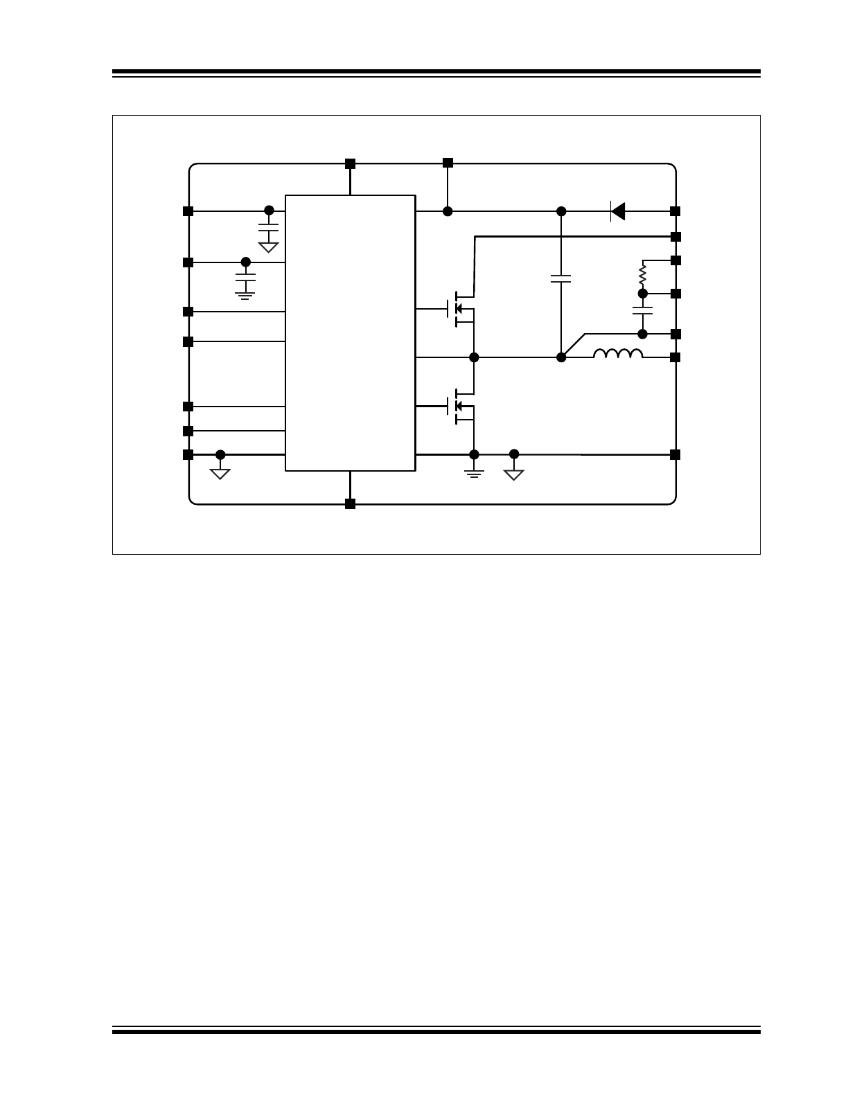
Functional Block Diagram
PWM
CONTROLLER
V
OUT
Q1
Q2
PV
IN
BST
EN
I
LIM
PV
DD
PGND
5V
DD
FREQ
PG
SW
GND
L1
C3
SW
DH
DL
V
IN
BST
ANODE
PGND
V
DD
AGND
PV
DD
I
LIM
PG
FB
FREQ
EN
FB
D1
V
IN
RIA
C4
C1
C2
R1
RIB

MIC45208-1/-2
DS20005603A-page 4
2017 Microchip Technology Inc.
1.0
ELECTRICAL CHARACTERISTICS
Absolute Maximum Ratings
†
V
PVIN
, V
VIN
to PGND................................................................................................................................. –0.3V to +30V
V
PVDD
, V
5VDD
, V
ANODE
to PGND ................................................................................................................ –0.3V to +6V
V
SW
, V
FREQ
, V
ILIM
, V
EN
to PGND .................................................................................................. –0.3V to (V
IN
+ 0.3V)
V
BST
to V
SW
................................................................................................................................................. –0.3V to +6V
V
BST
to PGND
.......................................................................................................................................... –0.3V to +36V
V
PG
to PGND ............................................................................................................................. –0.3V to (5 V
DD
+ 0.3V)
V
FB
, V
RIB
to PGND..................................................................................................................... –0.3V to (5 V
DD
+ 0.3V)
PGND to GND.......................................................................................................................................... –0.3V to +0.3V
Junction Temperature........................................................................................................................................... +150°C
Storage Temperature (T
S
) ..................................................................................................................... –65°C to +150°C
Lead Temperature (soldering, 10s) ...................................................................................................................... +260°C
ESD Rating ............................................................................................................................................... ESD Sensitive
Operating Ratings
(
1
)
Supply Voltage (V
PVIN,
V
VIN
) ......................................................................................................................... 4.5V to 26V
Output Current ........................................................................................................................................................... 10A
Enable Input (V
EN
) ............................................................................................................................................ 0V to V
IN
Power-Good (V
PG
) ......................................................................................................................................... 0V to 5V
DD
Junction Temperature (T
J
)..................................................................................................................... –40°C to +125°C
Junction Thermal Resistance
(
2
)
10 mm x 10 mm x 4 mm QFN-52 (
JA
) ...........................................................................................................16.6°C/W
10 mm x 10 mm 4 mm QFN-52 (
JC
) ...................................................................................................................4°C/W
Note 1:
The device is not ensured to function outside the operating range.
2:
JA
and
JC
were measured using the MIC45208 evaluation board.
†
Notice:
Stresses above those listed under “Maximum Ratings” may cause permanent damage to the device. This
is a stress rating only and functional operation of the device at those or any other conditions above those indi-
cated in the operational sections of this specification is not intended. Exposure to maximum rating conditions for
extended periods may affect device reliability.

2017 Microchip Technology Inc.
DS20005603A-page 5
MIC45208-1/-2
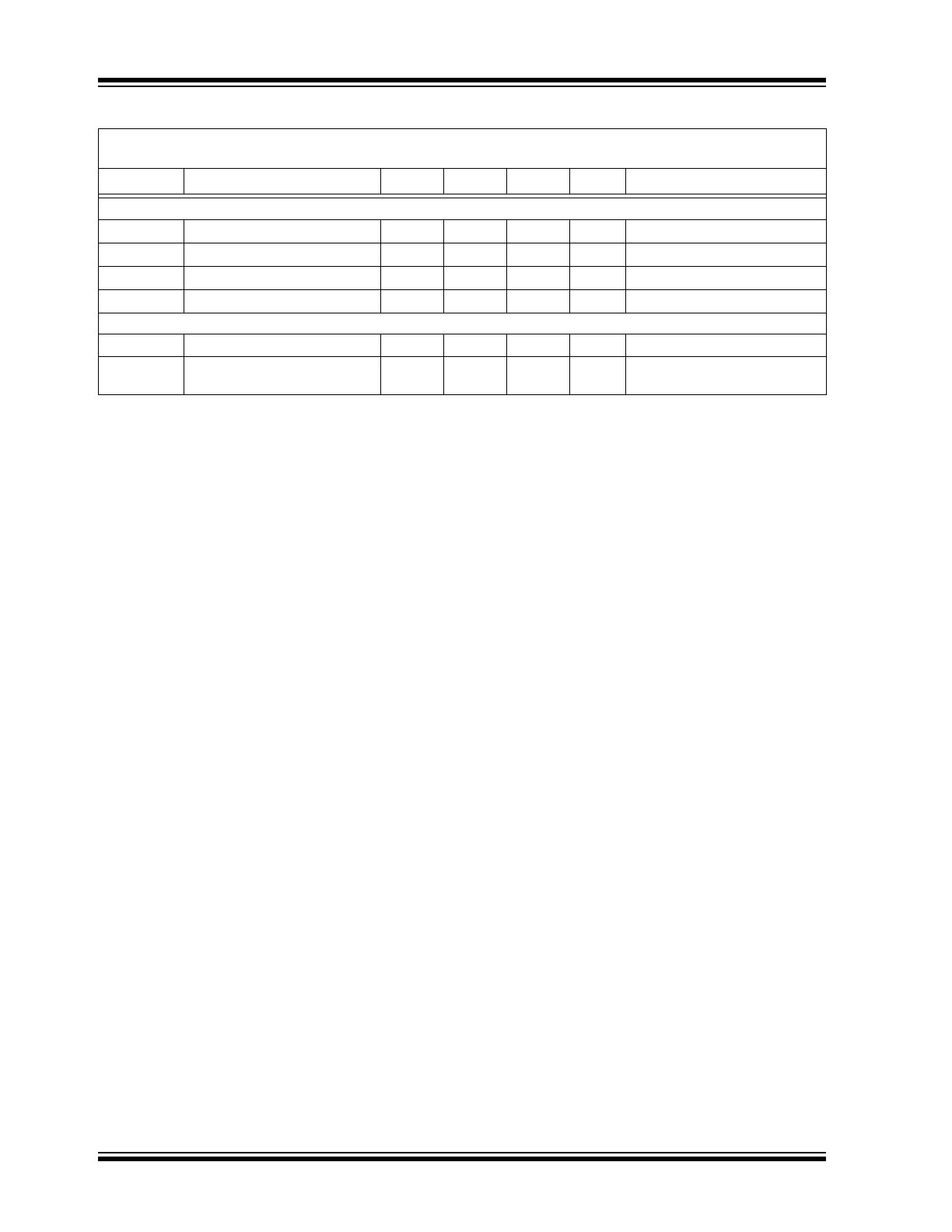
TABLE 1-1:
ELECTRICAL CHARACTERISTICS
(
1
)
Electrical Specifications:
unless otherwise specified, PV
IN
= V
IN
= V
EN
= 12V; V
OUT
= 3.3V; V
BST
– V
SW
= 5V;
T
J
= +25°C. Boldface values indicate –40°C
T
J
+125°C.
Symbol
Parameter
Min.
Typ.
Max.
Units
Test Conditions
Power Supply Input
V
IN
, PV
IN
Input Voltage Range
4.5
—
26
V
—
I
Q
Quiescent Supply Current
(MIC45208-1)
—
—
0.75
mA
V
FB
= 1.5V
I
Q
Quiescent Supply Current
(MIC45208-2)
—
2.1
3
mA
V
FB
= 1.5V
I
IN
Operating Current:
MIC45208-1
—
0.4
—
mA
V
PVIN
= V
IN
= 12V,
V
OUT
= 1.8V, I
OUT
= 0A,
f
SW
= 600 kHz
MIC45208-2
—
43
—
I
SHDN
Shutdown Supply Current
—
4
10
µA
SW = Unconnected, V
EN
= 0V
5V
DD
Output
V
DD
5V
DD
Output Voltage
4.8
5.1
5.4
V
V
IN
= 7V to 26V, I
5VDD
= 10 mA
UVLO
5V
DD
UVLO Threshold
3.8
4.2
4.6
V
V
5VDD
Rising
UVLO_HYS 5V
DD
UVLO Hysteresis
—
400
—
mV
V
5VDD
Falling
V
DD(LR)
LDO Load Regulation
0.6
2
3.6
%
I
5VDD
= 0 to 40 mA
Reference
V
FB
Feedback Reference Voltage
0.792
0.8
0.808
V
T
J
= +25°C
0.784
0.8
0.816
–40°C
T
J
+125°C
I
FB_BIAS
Feedback Bias Current
—
5
500
nA
V
FB
= 0.8V
Enable Control
EN
HIGH
EN Logic Level High
1.8
—
—
V
—
EN
LOW
EN Logic level Low
—
—
0.6
V
—
EN
HYS
EN Hysteresis
—
200
—
mV
—
I
ENBIAS
EN Bias Current
—
5
10
µA
V
EN
= 12V
Oscillator
f
SW
Switching Frequency
400
600
750
kHz
V
FREQ
= V
IN,
I
OUT
= 2A
—
350
—
V
FREQ
= 50% V
IN,
I
OUT
= 2A
D
MAX
Maximum Duty Cycle
—
85
—
%
—
D
MIN
Minimum Duty Cycle
—
0
—
%
V
FB
= 1V
t
OFF(MIN)
Minimum OFF-Time
140
200
260
ns
—
Soft Start
t
SS
Soft Start Time
—
3
—
ms
FB from 0V to 0.8V
Short-Circuit Protection
V
CL_OFFSET
Current-Limit Threshold
–30
–14
0
mV
V
FB
= 0.79V
V
SC
Short-Circuit Threshold
–23
–7
9
mV
V
FB
= 0V
I
CL
Current-Limit Source Current
50
70
90
µA
V
FB
= 0.79V
I
SC
Short-Circuit Source Current
25
35
45
µA
V
FB
= 0V
Leakage
I
SW_Leakage
SW, BST Leakage Current
—
—
10
µA
—
I
FREQ_LEAK
FREQ Pin Leakage Current
—
—
10
µA
—
Note 1:
Specification for packaged product only.
MIC45208-1/-2
DS20005603A-page 6
2017 Microchip Technology Inc.
Power Good (PG)
V
PG_TH
PG Threshold Voltage
85
90
95
%V
OUT
Sweep V
FB
from Low-to-High
V
PG_HYS
PG Hysteresis
—
6
—
%V
OUT
Sweep V
FB
from High-to-Low
t
PG_DLY
PG Delay Time
—
100
—
µs
Sweep V
FB
from Low-to-High
V
PG_LOW
PG Low Voltage
—
70
200
mV
V
FB
< 90% x V
NOM
, I
PG
= 1 mA
Thermal Protection
T
SHD
Overtemperature Shutdown
—
160
—
°C
T
J
Rising
T
SHD_HYS
Overtemperature Shutdown
Hysteresis
—
15
—
°C
—
TABLE 1-1:
ELECTRICAL CHARACTERISTICS
(
1
)
(CONTINUED)
Electrical Specifications:
unless otherwise specified, PV
IN
= V
IN
= V
EN
= 12V; V
OUT
= 3.3V; V
BST
– V
SW
= 5V;
T
J
= +25°C. Boldface values indicate –40°C
T
J
+125°C.
Symbol
Parameter
Min.
Typ.
Max.
Units
Test Conditions
Note 1:
Specification for packaged product only.
2017 Microchip Technology Inc.
DS20005603A-page 7
MIC45208-1/-2
2.0
TYPICAL PERFORMANCE CURVES
Note:
Unless otherwise indicated, V
IN
= 12V, f
SW
= 600 kHz, T
J
= +25°C.
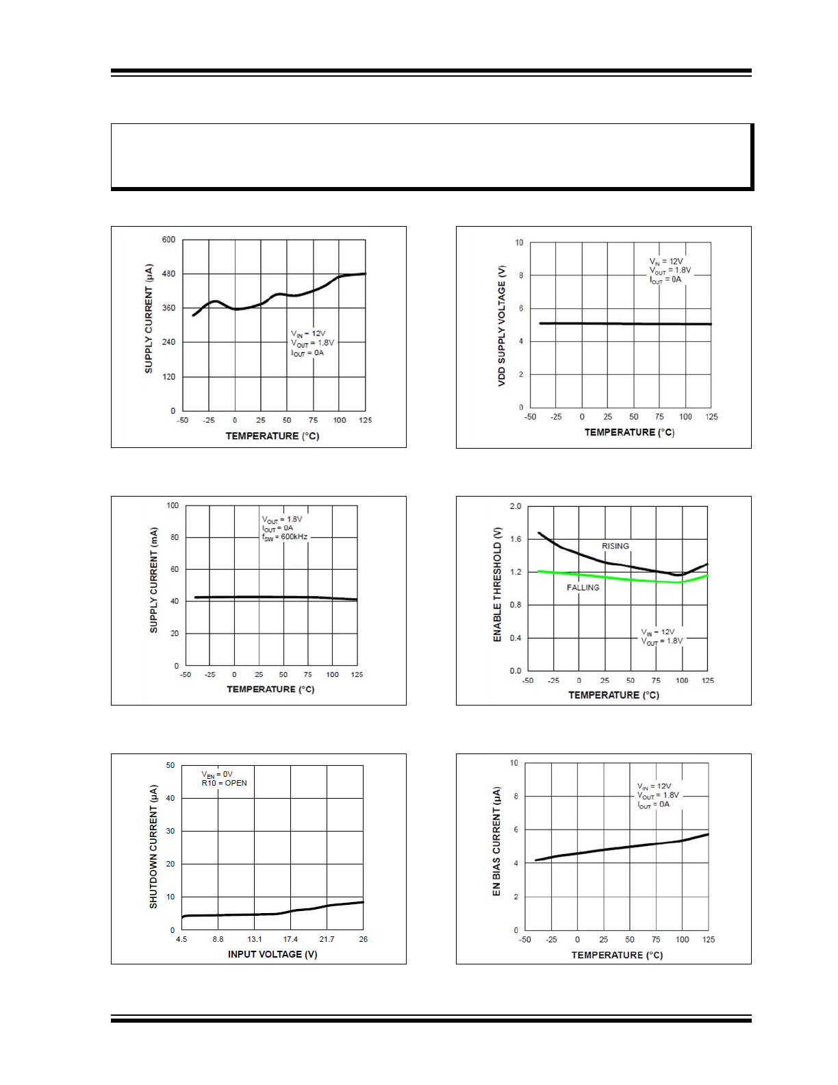
FIGURE 2-1:
V
IN
Operating Supply
Current vs. Temperature (MIC45208-1).
FIGURE 2-2:
V
IN
Operating Supply
Current vs. Temperature (MIC45208-2).
FIGURE 2-3:
V
IN
Shutdown Current vs.
Input Voltage.
FIGURE 2-4:
V
DD
Supply Voltage vs.
Temperature.
FIGURE 2-5:
Enable Threshold vs.
Temperature.
FIGURE 2-6:
EN Bias Current vs.
Temperature.
Note:
The graphs and tables provided following this note are a statistical summary based on a limited number of
samples and are provided for informational purposes only. The performance characteristics listed herein
are not tested or guaranteed. In some graphs or tables, the data presented may be outside the specified
operating range (e.g., outside specified power supply range) and therefore outside the warranted range.
MIC45208-1/-2
DS20005603A-page 8
2017 Microchip Technology Inc.
Note:
Unless otherwise indicated, V
IN
= 12V, f
SW
= 600 kHz, T
J
= +25°C.
FIGURE 2-7:
Feedback Voltage vs.
Temperature.
FIGURE 2-8:
Output Voltage
vs.Temperature.
FIGURE 2-9:
Switching Frequency
vs.Temperature.
FIGURE 2-10:
Output Peak Current-Limit
vs. Temperature.
FIGURE 2-11:
Efficiency (V
IN
= 5V) vs.
Output Current (MIC45208-1).
FIGURE 2-12:
Efficiency (V
IN
= 12V) vs.
Output Current (MIC45208-1).
2017 Microchip Technology Inc.
DS20005603A-page 9
MIC45208-1/-2
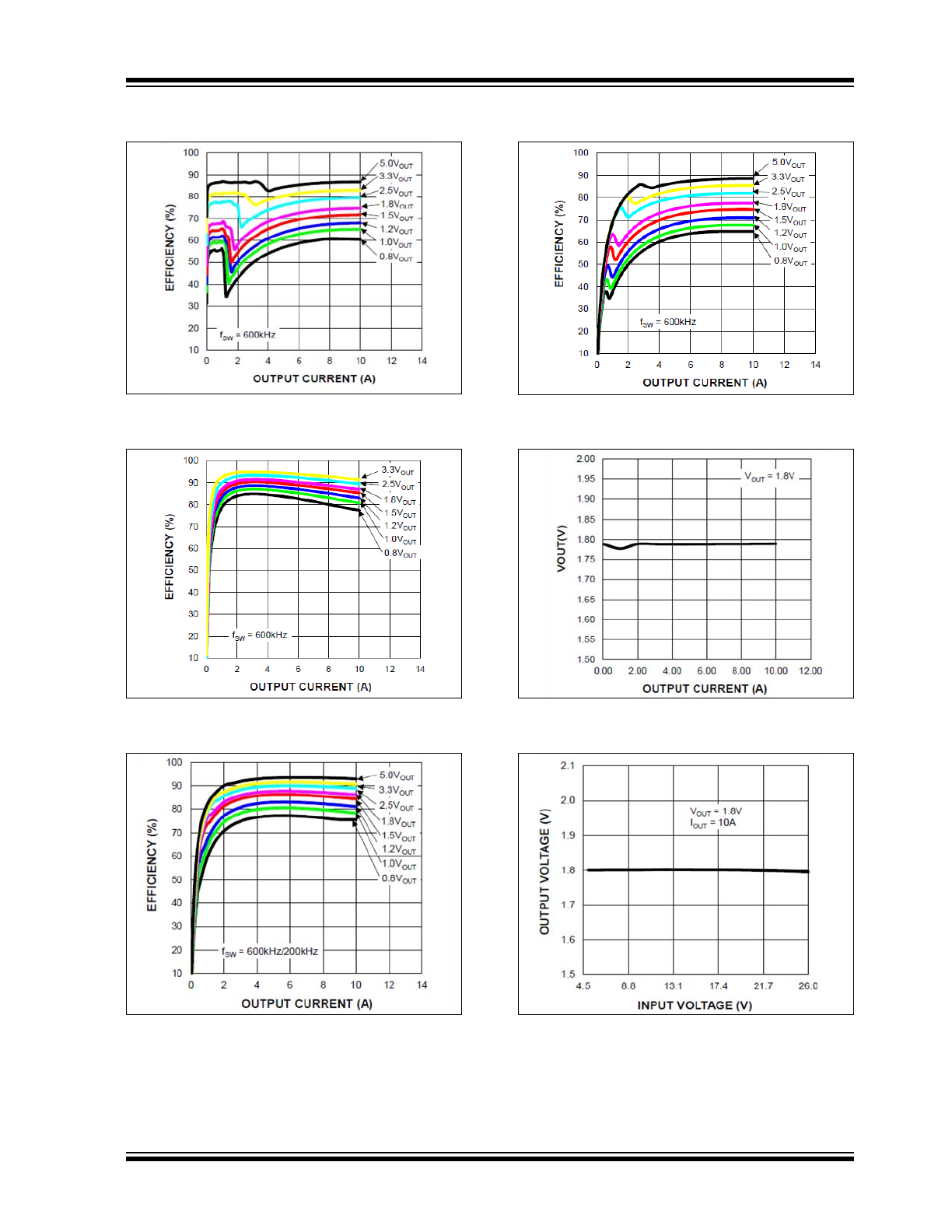
Note:
Unless otherwise indicated, V
IN
= 12V, f
SW
= 600 kHz, T
J
= +25°C.
FIGURE 2-13:
Efficiency (V
IN
= 24V) vs.
Output Current (MIC45208-1).
FIGURE 2-14:
Efficiency (V
IN
= 5V) vs.
Output Current (MIC45208-2).
FIGURE 2-15:
Efficiency (V
IN
= 12V) vs.
Output Current (MIC45208-2).
FIGURE 2-16:
Efficiency (V
IN
= 24V) vs.
Output Current (MIC45208-2).
FIGURE 2-17:
Load Regulation vs. Input
Voltage.
FIGURE 2-18:
Line Regulation.
MIC45208-1/-2
DS20005603A-page 10
2017 Microchip Technology Inc.
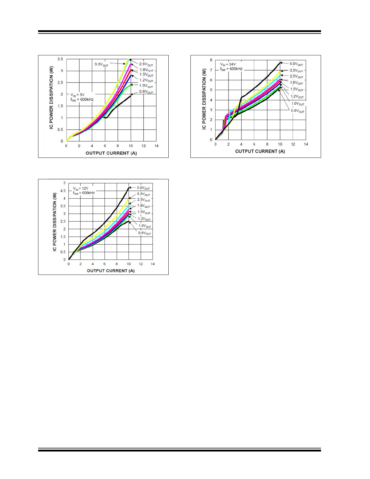
Note:
Unless otherwise indicated, V
IN
= 12V, f
SW
= 600 kHz, T
J
= +25°C.
FIGURE 2-19:
IC Power Dissipation
(V
IN
= 5V) vs. Output Current (MIC-45208-1).
FIGURE 2-20:
IC Power Dissipation
(V
IN
= 12V) vs. Output Current (MIC45208-1).
FIGURE 2-21:
IC Power Dissipation
(V
IN
= 24V) vs. Output Current (MIC45208-1).