
2010 Microchip Technology Inc.
DS22065C-page 1
25LC512
Device Selection Table
Features:
• 20 MHz max. Clock Speed
• Byte and Page-level Write Operations:
- 128-byte page
- 5 ms max.
- No page or sector erase required
• Low-Power CMOS Technology:
- Max. Write Current: 5 mA at 5.5V, 20 MHz
- Read Current: 10 mA at 5.5V, 20 MHz
- Standby Current: 1
A at 2.5V (Deep power-
down)
• Electronic Signature for Device ID
• Self-Timed Erase and Write cycles:
- Page Erase (5 ms, typical)
- Sector Erase (10 ms/sector, typical)
- Bulk Erase (10 ms, typical)
• Sector Write Protection (16K byte/sector):
- Protect none, 1/4, 1/2 or all of array
• Built-In Write Protection:
- Power-on/off data protection circuitry
- Write enable latch
- Write-protect pin
• High Reliability:
- Endurance: 1 Million erase/write cycles
- Data Retention: >200 years
- ESD Protection: >4000V
• Temperature Ranges Supported:
• Pb-free and RoHS Compliant
Pin Function Table
Description:
The Microchip Technology Inc. 25LC512 is a 512 Kbit
serial EEPROM memory with byte-level and page-level
serial EEPROM functions. It also features Page, Sector
and Chip erase functions typically associated with
Flash-based products. These functions are not required
for byte or page write operations. The memory is
accessed via a simple Serial Peripheral Interface (SPI)
compatible serial bus. The bus signals required are a
clock input (SCK) plus separate data in (SI) and data out
(SO) lines. Access to the device is controlled by a Chip
Select (CS) input.
Communication to the device can be paused via the
hold pin (HOLD). While the device is paused, transi-
tions on its inputs will be ignored, with the exception of
Chip Select, allowing the host to service higher priority
interrupts.
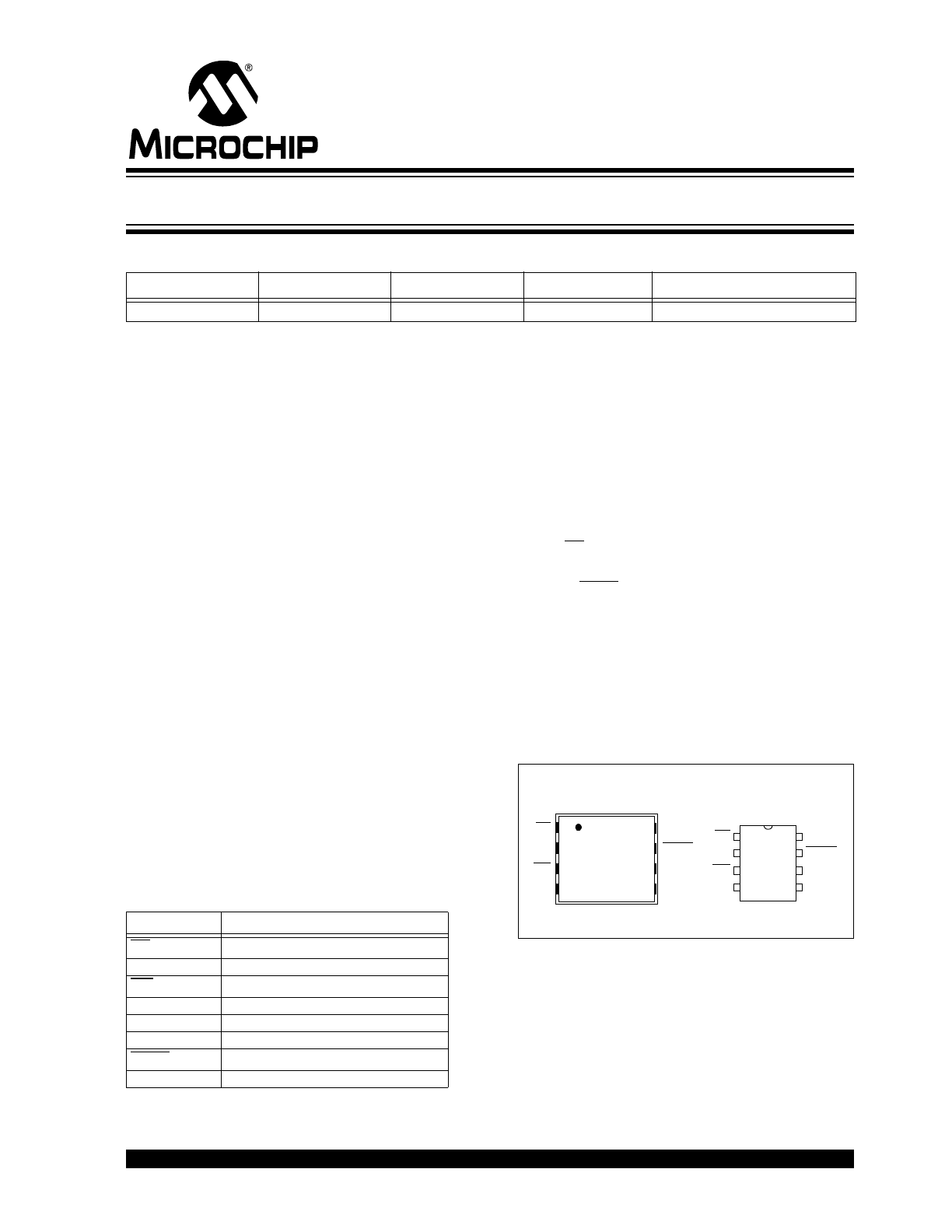
The 25LC512 is available in standard packages includ-
ing 8-lead PDIP, SOIC, and advanced 8-lead DFN
package. All packages are Pb-free and RoHS
compliant.
Package Types (not to scale)
Part Number
V
CC
Range
Page Size
Temp. Ranges
Packages
25LC512
2.5-5.5V
128 Byte
I,E
P, SN, SM, MF
- Industrial (I):
-40
C to +85C
- Automotive (E):
-40°C to +125°C
Name
Function
CS
Chip Select Input
SO
Serial Data Output
WP
Write-Protect
V
SS
Ground
SI
Serial Data Input
SCK
Serial Clock Input
HOLD
Hold Input
V
CC
Supply Voltage
25L
C512
CS
SO
WP
V
SS
1
2
3
4
8
7
6
5
V
CC
HOLD
SCK
SI
PDIP/SOIC/SOIJ
(P, SN, SM)
DFN
CS
SO
WP
V
SS
HOLD
SCK
SI
25L
C512
5
6
7
8
4
3
2
1
V
CC
(MF)
512 Kbit SPI Bus Serial EEPROM
25LC512
DS22065C-page 2
2010 Microchip Technology Inc.
1.0
ELECTRICAL CHARACTERISTICS
Absolute Maximum Ratings
(†)
V
CC
.............................................................................................................................................................................6.5V
All inputs and outputs w.r.t. V
SS
......................................................................................................... -0.6V to V
CC
+1.0V
Storage temperature .................................................................................................................................-65°C to 150°C
Ambient temperature under bias ...............................................................................................................-40°C to 125°C
ESD protection on all pins ..........................................................................................................................................4 kV
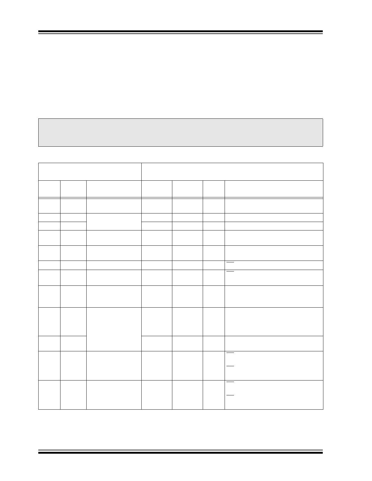
TABLE 1-1:
DC CHARACTERISTICS
† NOTICE: Stresses above those listed under “Absolute Maximum Ratings” may cause permanent damage to the
device. This is a stress rating only and functional operation of the device at those or any other conditions above those
indicated in the operational listings of this specification is not implied. Exposure to maximum rating conditions for an
extended period of time may affect device reliability.
DC CHARACTERISTICS
Industrial (I):
T
A
= -40°C to +85°C
V
CC
= 2.5V to 5.5V
Automotive (E):
T
A
= -40°C to +125°C
V
CC
= 2.5V to 5.5V
Param.
No.
Sym.
Characteristic
Min.
Max.
Units
Test Conditions
D001
V
IH
1
High-level input
voltage
.7 V
CC
V
CC
+1
V
D002
V
IL
1
Low-level input
voltage
-0.3
0.3 V
CC
V
V
CC
2.7V
D003
V
IL
2
-0.3
0.2 V
CC
V
V
CC
< 2.7V
D004
V
OL
Low-level output
voltage
—
0.4
V
I
OL
= 2.1 mA
D005
V
OH
High-level output
voltage
V
CC
-0.2
—
V
I
OH
= -400
A
D006
I
LI
Input leakage current
—
±1
A
CS = V
CC
, V
IN
= V
SS
or V
CC
D007
I
LO
Output leakage
current
—
±1
A
CS = V
CC
, V
OUT
= V
SS
or V
CC
D008
C
INT
Internal capacitance
(all inputs and
outputs)
—
7
pF
T
A
= 25°C, CLK = 1.0 MHz,
V
CC
= 5.0V (Note)
D009
I
CC
Read
Operating current
—
—
10
5
mA
mA
V
CC
= 5.5V; F
CLK
= 20.0 MHz;
SO = Open
V
CC
= 2.5V; F
CLK
= 10.0 MHz;
SO = Open
D010
I
CC
Write
—
—
7
5
mA
mA
V
CC
= 5.5V
V
CC
= 2.5V
D011
I
CCS
Standby current
—
—
20
10
A
A
CS = V
CC
= 5.5V, Inputs tied to V
CC
or
V
SS
, 125°C
CS = V
CC
= 5.5V, Inputs tied to V
CC
or
V
SS
, 85°C
D012
I
CCSPD
Deep power-down
current
—
2
1
A
A
CS = V
CC
= 2.5V, Inputs tied to V
CC
or
V
SS
, 125°C
CS = V
CC
= 2.5V, Inputs tied to V
CC
or
V
SS
, 85°C
Note:
This parameter is periodically sampled and not 100% tested.
2010 Microchip Technology Inc.
DS22065C-page 3
25LC512
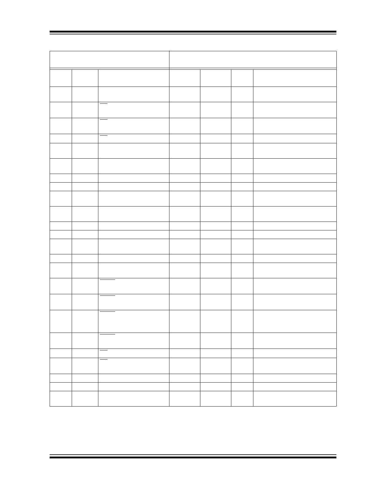
TABLE 1-2:
AC CHARACTERISTICS
AC CHARACTERISTICS
Industrial (I):
T
A
= -40°C to +85°C
V
CC
= 2.0V to 5.5V
Automotive (E):
T
A
= -40°C to +125°C
V
CC
= 2.5V to 5.5V
Param.
No.
Sym.
Characteristic
Min.
Max.
Units
Conditions
1
F
CLK
Clock frequency
—
—
20
10
MHz
MHz
4.5V
V
CC
5.5V (I)
2.5V
V
CC
5.5V (I, E)
2
T
CSS
CS setup time
25
50
—
—
ns
ns
4.5V
V
CC
5.5V (I)
2.5V
V
CC
5.5V (I, E)
3
T
CSH
CS hold time
50
100
—
—
ns
ns
4.5V
V
CC
5.5V (I)
2.5V
V
CC
5.5V (I, E)
4
T
CSD
CS disable time
50
—
ns
—
5
Tsu
Data setup time
5
10
—
—
ns
ns
4.5V
V
CC
5.5V (I)
2.5V
V
CC
5.5V (I, E)
6
T
HD
Data hold time
10
20
—
—
ns
ns
4.5V
V
CC
5.5V (I)
2.5V
V
CC
5.5V (I, E)
7
T
R
CLK rise time
—
20
ns
(Note 1)
8
T
F
CLK fall time
—
20
ns
(Note 1)
9
T
HI
Clock high time
25
50
—
—
ns
ns
4.5V
V
CC
5.5V (I)
2.5V
V
CC
5.5V (I, E)
10
T
LO
Clock low time
25
50
—
—
ns
ns
4.5V
V
CC
5.5V (I)
2.5V
V
CC
5.5V (I, E)
11
T
CLD
Clock delay time
50
—
ns
—
12
T
CLE
Clock enable time
50
—
ns
—
13
T
V
Output valid from clock low
—
—
25
50
ns
ns
4.5V
V
CC
5.5V (I)
2.5V
V
CC
5.5V (I, E)
14
T
HO
Output hold time
0
—
ns
(Note 1)
15
T
DIS
Output disable time
—
—
25
50
ns
ns
4.5V
V
CC
5.5V (I)
2.5V
V
CC
5.5V (I, E)
16
T
HS
HOLD setup time
10
20
—
—
ns
ns
4.5V
V
CC
5.5V (I)
2.5V
V
CC
5.5V (I, E)
17
T
HH
HOLD hold time
10
20
—
—
ns
ns
4.5V
V
CC
5.5V (I)
2.5V
V
CC
5.5V (I, E)
18
T
HZ
HOLD low to output
High-Z
15
30
—
—
ns
ns
4.5V
V
CC
5.5V (I)
2.5V
V
CC
5.5V (I, E)
(Note 1)
19
T
HV
HOLD high to output valid
15
30
—
—
ns
ns
4.5V
V
CC
5.5V (I)
2.5V
V
CC
5.5V (I, E)
20
T
REL
CS High to Standby mode
—
100
s
—
21
T
PD
CS High to Deep power-
down
—
100
s
—
22
T
CE
Chip erase cycle time
—
10
ms
—
23
T
SE
Sector erase cycle time
—
10
ms
—
24
T
WC
Internal write cycle time
—
5
ms
Byte or Page mode and Page
Erase
Note 1: This parameter is periodically sampled and not 100% tested.
2: This parameter is not tested but established by characterization and qualification. For endurance
estimates in a specific application, please consult the Total Endurance™ Model, which can be obtained
from Microchip’s web site at www.microchip.com.

25LC512
DS22065C-page 4
2010 Microchip Technology Inc.
TABLE 1-3:
AC TEST CONDITIONS
25
—
Endurance
1M
—
E/W
Cycles
Page mode, 25°C, 5.5V (Note 2)
TABLE 1-2:
AC CHARACTERISTICS (CONTINUED)
AC CHARACTERISTICS
Industrial (I):
T
A
= -40°C to +85°C
V
CC
= 2.0V to 5.5V
Automotive (E):
T
A
= -40°C to +125°C
V
CC
= 2.5V to 5.5V
Param.
No.
Sym.
Characteristic
Min.
Max.
Units
Conditions
Note 1: This parameter is periodically sampled and not 100% tested.
2: This parameter is not tested but established by characterization and qualification. For endurance
estimates in a specific application, please consult the Total Endurance™ Model, which can be obtained
from Microchip’s web site at www.microchip.com.
AC Waveform:
V
LO
= 0.2V
—
V
HI
= V
CC
- 0.2V
(Note 1)
V
HI
= 4.0V
(Note 2)
C
L
= 30 pF
—
Timing Measurement Reference Level
Input
0.5 V
CC
Output
0.5 V
CC
Note 1: For V
CC
4.0V
2: For V
CC
> 4.0V
2010 Microchip Technology Inc.
DS22065C-page 5
25LC512
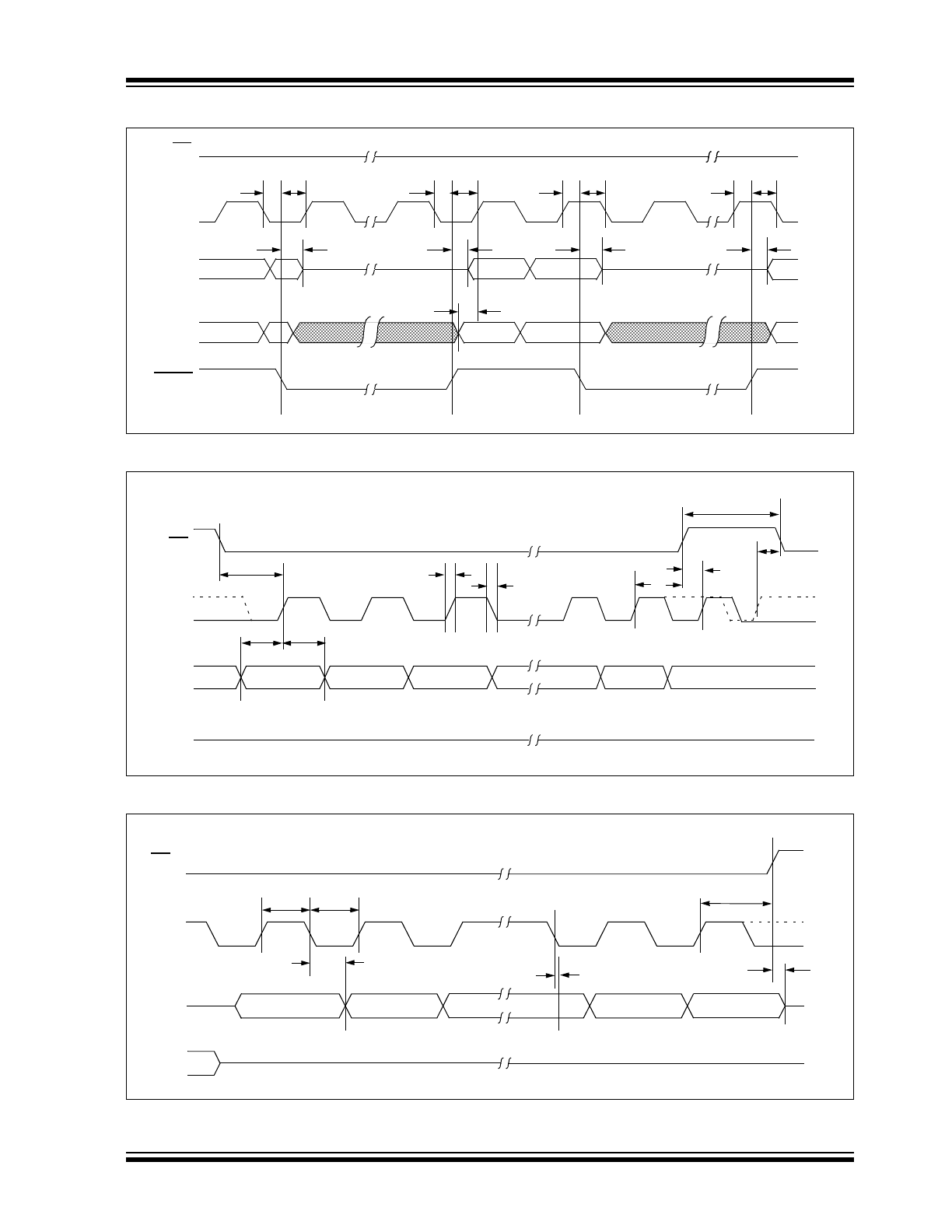
FIGURE 1-1:
HOLD TIMING
FIGURE 1-2:
SERIAL INPUT TIMING
FIGURE 1-3:
SERIAL OUTPUT TIMING
CS
SCK
SO
SI
HOLD
17
16
16
17
19
18
Don’t Care
5
High-Impedance
n + 1
n
n - 1
n
n
n - 1
17
16
17
16
19
18
High-Impedance
n - 2
n + 1
n
n - 2
Don’t Care
CS
SCK
SI
SO
6
5
8
7
11
3
LSB in
MSB in
High-Impedance
12
Mode 1,1
Mode 0,0
2
4
CS
SCK
SO
10
9
13
MSB out
LSB out
3
15
Don’t Care
SI
Mode 1,1
Mode 0,0
14
25LC512
DS22065C-page 6
2010 Microchip Technology Inc.
2.0
FUNCTIONAL DESCRIPTION
2.1
Principles of Operation
The 25LC512 is a 65,536 byte Serial EEPROM
designed to interface directly with the Serial Periph-
eral Interface (SPI) port of many of today’s popular
microcontroller families, including Microchip’s PIC
®
microcontrollers. It may also interface with microcon-
trollers that do not have a built-in SPI port by using
discrete I/O lines programmed properly in firmware to
match the SPI protocol.
The 25LC512 contains an 8-bit instruction register. The
device is accessed via the SI pin, with data being
clocked in on the rising edge of SCK. The CS pin must
be low and the HOLD pin must be high for the entire
operation.
Table 2-1 contains a list of the possible instruction
bytes and format for device operation. All instructions,
addresses, and data are transferred MSB first, LSB
last.
Data (SI) is sampled on the first rising edge of SCK
after CS goes low. If the clock line is shared with other
peripheral devices on the SPI bus, the user can assert
the HOLD input and place the 25LC512 in ‘HOLD’
mode. After releasing the HOLD pin, operation will
resume from the point when the HOLD was asserted.
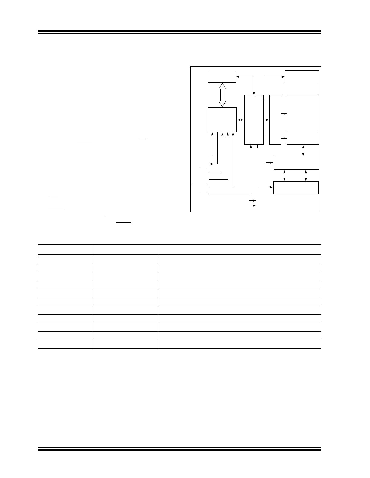
BLOCK DIAGRAM
TABLE 2-1:
INSTRUCTION SET
SI
SO
SCK
CS
HOLD
WP
STATUS
Register
I/O Control
Memory
Control
Logic
X
Dec
HV Generator
EEPROM
Array
Page Latches
Y Decoder
Sense Amp.
R/W Control
Logic
V
CC
V
SS
Instruction Name
Instruction Format
Description
READ
0000 0011
Read data from memory array beginning at selected address
WRITE
0000 0010
Write data to memory array beginning at selected address
WREN
0000 0110
Set the write enable latch (enable write operations)
WRDI
0000 0100
Reset the write enable latch (disable write operations)
RDSR
0000 0101
Read STATUS register
WRSR
0000 0001
Write STATUS register
PE
0100 0010
Page Erase – erase one page in memory array
SE
1101 1000
Sector Erase – erase one sector in memory array
CE
1100 0111
Chip Erase – erase all sectors in memory array
RDID
1010 1011
Release from Deep power-down and read electronic signature
DPD
1011 1001
Deep Power-Down mode
2010 Microchip Technology Inc.
DS22065C-page 7
25LC512
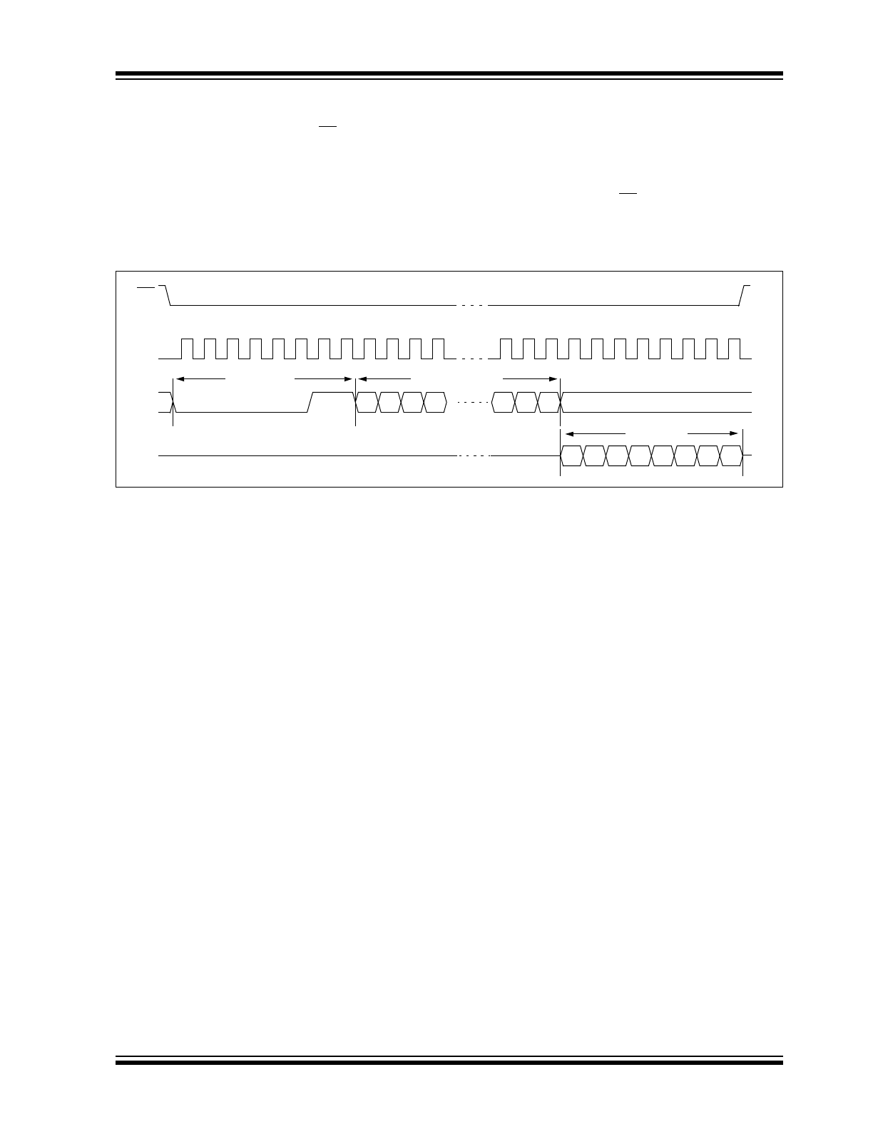
Read Sequence
The device is selected by pulling CS low. The 8-bit
READ instruction is transmitted to the 25LC512 fol-
lowed by the 16-bit address. After the correct READ
instruction and address are sent, the data stored in the
memory at the selected address is shifted out on the
SO pin. The data stored in the memory at the next
address can be read sequentially by continuing to
provide clock pulses. The internal Address Pointer is
automatically incremented to the next higher address
after each byte of data is shifted out. When the highest
address is reached (FFFFh), the address counter rolls
over to address 0000h allowing the read cycle to be
continued indefinitely. The READ instruction is
terminated by raising the CS pin (Figure 2-1).
FIGURE 2-1:
READ SEQUENCE
SO
SI
SCK
CS
0
2
3
4
5
6
7
8
9 10 11
21 22 23 24 25 26 27 28 29 30 31
1
0
1
0
0
0
0
0
1
15 14 13 12
2
1
0
7
6
5
4
3
2
1
0
Instruction
16-bit Address
Data Out
High-Impedance
25LC512
DS22065C-page 8
2010 Microchip Technology Inc.
2.2
Write Sequence
Prior to any attempt to write data to the 25LC512, the
write enable latch must be set by issuing the WREN
instruction (Figure 2-4). This is done by setting CS low
and then clocking out the proper instruction into the
25LC512. After all eight bits of the instruction are trans-
mitted, the CS must be brought high to set the write
enable latch. If the write operation is initiated immedi-
ately after the WREN instruction without CS being
brought high, the data will not be written to the array
because the write enable latch will not have been
properly set.
A write sequence includes an automatic, self timed
erase cycle. It is not required to erase any portion of the
memory prior to issuing a WRITE instruction.
Once the write enable latch is set, the user may
proceed by setting the CS low, issuing a WRITE instruc-
tion, followed by the 16-bit address, and then the data
to be written. Up to 128 bytes of data can be sent to the
device before a write cycle is necessary. The only
restriction is that all of the bytes must reside in the
same page.
For the data to be actually written to the array, the CS
must be brought high after the Least Significant bit (D0)
of the n
th
data byte has been clocked in. If CS is
brought high at any other time, the write operation will
not be completed. Refer to Figure 2-2 and Figure 2-3
for more detailed illustrations on the byte write
sequence and the page write sequence, respectively.
While the write is in progress, the STATUS register may
be read to check the status of the WPEN, WIP, WEL,
BP1 and BP0 bits (Figure 2-6). A read attempt of a
memory array location will not be possible during a
write cycle. When the write cycle is completed, the
write enable latch is reset.
FIGURE 2-2:
BYTE WRITE SEQUENCE
Note:
When doing a write of less than 128 bytes
the data in the rest of the page is refreshed
along with the data bytes being written.
This will force the entire page to endure a
write cycle, for this reason endurance is
specified per page.
Note:
Page write operations are limited to writing
bytes within a single physical page,
regardless of the number of bytes
actually being written. Physical page
boundaries start at addresses that are
integer multiples of the page buffer size (or
‘page size’), and end at addresses that are
integer multiples of page size – 1. If a
Page Write command attempts to write
across a physical page boundary, the
result is that the data wraps around to the
beginning of the current page (overwriting
data previously stored there), instead of
being written to the next page as might be
expected. It is therefore necessary for the
application software to prevent page write
operations that would attempt to cross a
page boundary.
SO
SI
CS
9 10 11
21 22 23 24 25 26 27 28 29 30 31
0
0
0
0
0
0
0
1
15 14 13 12
2
1
0 7
6
5
4
3
2
1
0
Instruction
16-bit Address
Data Byte
High-Impedance
SCK
0
2
3
4
5
6
7
1
8
Twc
2010 Microchip Technology Inc.
DS22065C-page 9
25LC512
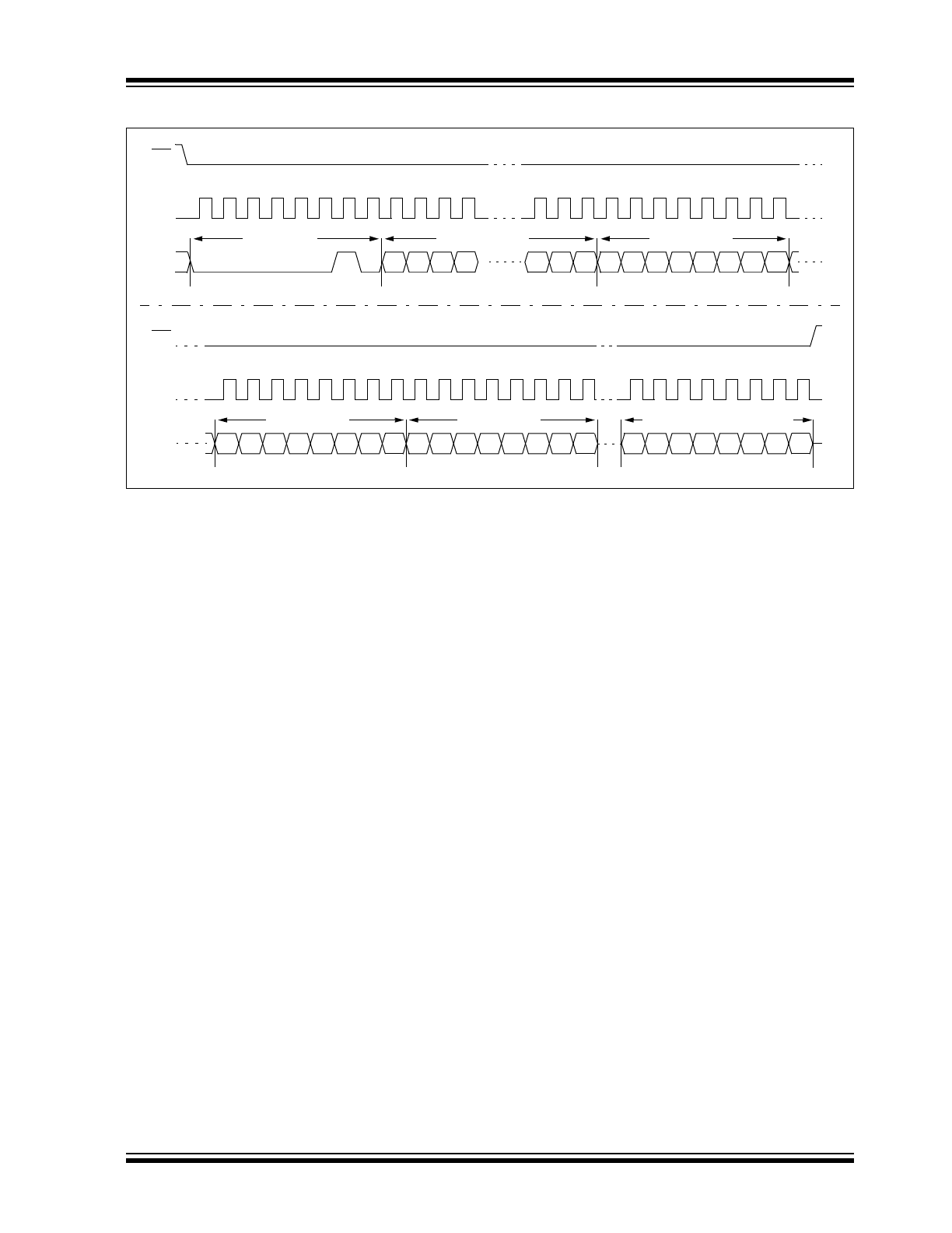
FIGURE 2-3:
PAGE WRITE SEQUENCE
SI
CS
9 10 11
21 22 23 24 25 26 27 28 29 30 31
0
0
0
0
0
0
0
1
15 14 13 12
2
1
0
7
6
5
4
3
2
1
0
Instruction
16-bit Address
Data Byte 1
SCK
0
2
3
4
5
6
7
1
8
SI
CS
41 42 43
46 47
7
6
5
4
3
2
1
0
Data Byte n (128 max)
SCK
32
34 35 36 37 38 39
33
40
7
6
5
4
3
2
1
0
Data Byte 3
7
6
5
4
3
2
1
0
Data Byte 2
44 45
25LC512
DS22065C-page 10
2010 Microchip Technology Inc.
2.3
Write Enable (WREN) and Write
Disable (WRDI)
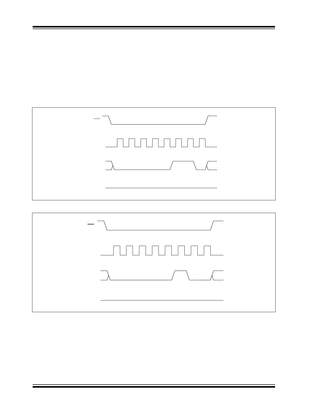
The 25LC512 contains a write enable latch. See
Table 2-4 for the Write-Protect Functionality Matrix.
This latch must be set before any write operation will be
completed internally. The WREN instruction will set the
latch, and the WRDI will reset the latch.
The following is a list of conditions under which the
write enable latch will be reset:
• Power-up
• WRDI instruction successfully executed
• WRSR instruction successfully executed
• WRITE instruction successfully executed
• PE instruction successfully executed
• SE instruction successfully executed
• CE instruction successfully executed
FIGURE 2-4:
WRITE ENABLE SEQUENCE (WREN)
FIGURE 2-5:
WRITE DISABLE SEQUENCE (WRDI)
SCK
0
2
3
4
5
6
7
1
SI
High-Impedance
SO
CS
0
1
0
0
0
0
0
1
SCK
0
2
3
4
5
6
7
1
SI
High-Impedance
SO
CS
0
1
0
0
0
0
0
10