
© 2009 Microchip Technology Inc.
Preliminary
DS22136B-page 1
25LC010A
25LC020A
25LC040A
Features:
• Max. Clock 5 MHz
• Low-Power CMOS Technology:
- Max. Write Current: 5 mA at 5.5V, 5 MHz
- Read Current: 5 mA at 5.5V, 5 MHz
- Standby Current: 10
μA at 5.5V
• 128 x 8 through 512 x 8-bit Organization
• Byte and Page-level Write Operations
• Self-Timed Erase and Write Cycles (6 ms max.)
• Block Write Protection:
- Protect none, 1/4, 1/2 or all of array
• Built-in Write Protection:
- Power-on/off data protection circuitry
- Write enable latch
- Write-protect pin
• Sequential Read
• High Reliability:
- Endurance: >1M erase/write cycles
- Data retention: > 200 years
- ESD protection: > 4000V
• Temperature Range Supported:
• Package is Pb-Free and RoHS Compliant
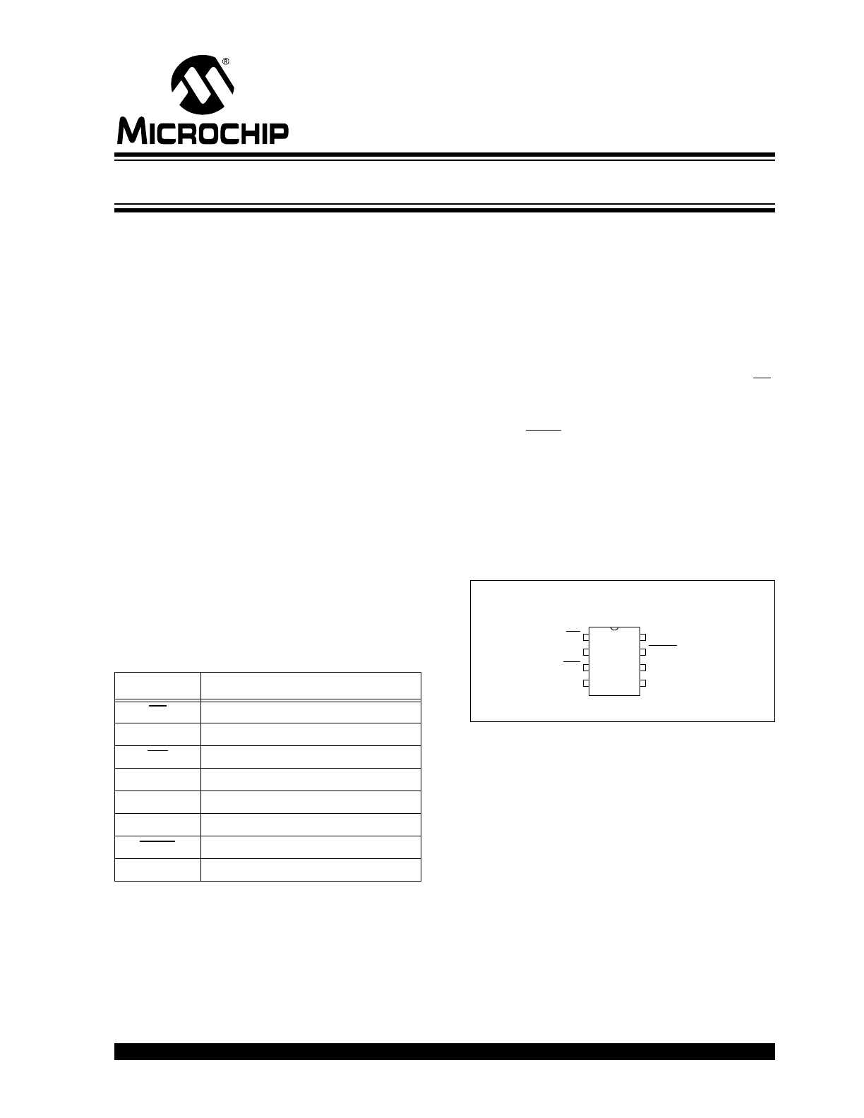
Pin Function Table
Description:
Microchip Technology Inc. 25LCXXXA* devices are
low-density 1 through 4 Kbit Serial Electrically Eras-
able PROMs (EEPROM). The devices are organized in
blocks of x8-bit memory and support the Serial Periph-
eral Interface (SPI) compatible serial bus architecture.
Byte-level and page-level functions are supported.
The bus signals required are a clock input (SCK) plus
separate data in (SI) and data out (SO) lines. Access to
the device is controlled through a Chip Select (CS)
input.
Communication to the device can be paused via the
hold pin (HOLD). While the device is paused, transi-
tions on its inputs will be ignored, with the exception of
Chip Select, allowing the host to service higher priority
interrupts.
The 25LCXXXA is available in a standard 8-lead SOIC
package. The package is Pb-free and RoHS
Compliant.
Package Types (not to scale)
- Extended (H):
-40°C to +150°C
Name
Function
CS
Chip Select Input
SO
Serial Data Output
WP
Write-Protect
V
SS
Ground
SI
Serial Data Input
SCK
Serial Clock Input
HOLD
Hold Input
V
CC
Supply Voltage
CS
SO
WP
V
SS
1
2
3
4
8
7
6
5
V
CC
HOLD
SCK
SI
SOIC
(SN)
1K-4K SPI Serial EEPROM High Temp Family Data Sheet
*25LCXXXA is used in this document as a generic part number for the 25 series devices.

25LCXXXA
DS22136B-page 2
Preliminary
© 2009 Microchip Technology Inc.
Device Selection Table
Part Number
Density
(bits)
Organization
V
CC
Range
Max. Speed
(MHz)
Page Size
(Bytes)
Temp.
Range
Package
25LC010A
1K
128 x 8
2.5V-5.5V
5
16
H
SN
25LC020A
2K
256 x 8
2.5V-5.5V
5
16
H
SN
25LC040A
4K
512 x 8
2.5V-5.5V
5
16
H
SN
© 2009 Microchip Technology Inc.
Preliminary
DS22136B-page 3
25LCXXXA
1.0
ELECTRICAL CHARACTERISTICS
Absolute Maximum Ratings
(†)
V
CC
............................................................................................................................................................................. 6.5V
All inputs and outputs w.r.t. V
SS
..........................................................................................................-0.6V to V
CC
+1.0V
Storage temperature ................................................................................................................................. -65°C to 155°C
Ambient temperature under bias........................................................................................................... -40°C to 150°C
(1)
ESD protection on all pins.......................................................................................................................................... 4 kV
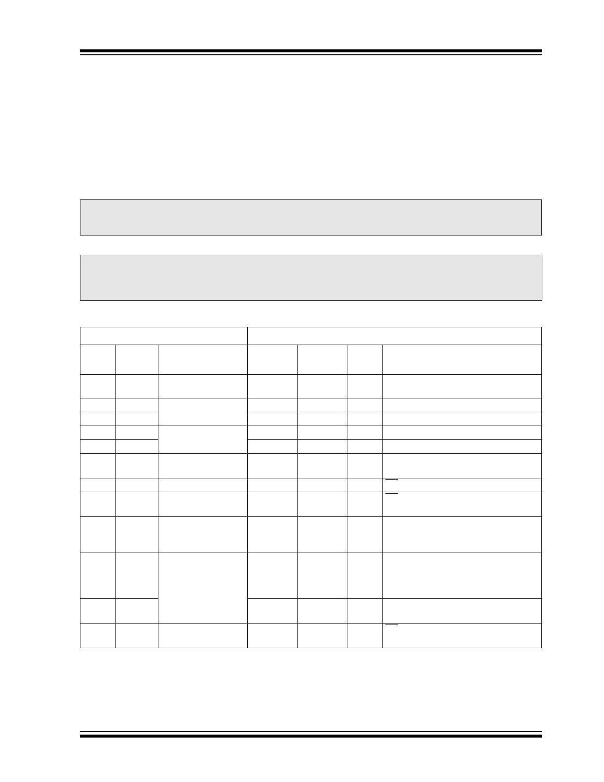
TABLE 1-1:
DC CHARACTERISTICS
Note 1: AEC-Q100 reliability testing for devices intended to operate at 150°C is 1,000 hours. Any design in which
the total operating time between 125°C and 150°C will be greater than 1,000 hours is not warranted with-
out prior written approval from Microchip Technology Inc.
† NOTICE: Stresses above those listed under “Absolute Maximum Ratings” may cause permanent damage to the
device. This is a stress rating only and functional operation of the device at those or any other conditions above those
indicated in the operational listings of this specification is not implied. Exposure to maximum rating conditions for an
extended period of time may affect device reliability.
DC CHARACTERISTICS
Extended (H):
T
A
= -40°C to +150°C
V
CC
= 2.5V to 5.5V
Param.
No.
Sym.
Characteristic
Min.
Max.
Units
Test Conditions
D001
V
IH
1
High-level input
voltage
.7 V
CC
V
CC
+1
V
D002
V
IL
1
Low-level input
voltage
-0.3
0.3V
CC
V
V
CC
≥ 2.7V
D003
V
IL
2
-0.3
0.2V
CC
V
V
CC
< 2.7V
D004
V
OL
Low-level output
voltage
—
0.4
V
I
OL
= 2.1 mA
D005
V
OL
—
0.2
V
I
OL
= 1.0 mA
D006
V
OH
High-level output
voltage
V
CC
-0.5
—
V
I
OH
= -400
μA
D007
I
LI
Input leakage current
—
±2
μA
CS = V
CC
, V
IN
= V
SS
OR
V
CC
D008
I
LO
Output leakage
current
—
±2
μA
CS = V
CC
, V
OUT
= V
SS
OR
V
CC
D009
C
INT
Internal Capacitance
(all inputs and
outputs)
—
7
pF
T
A
= 25°C, CLK = 1.0 MHz,
V
CC
= 5.0V (Note)
D010
I
CC
Read
Operating Current
—
—
5
2.5
mA
mA
V
CC
= 5.5V; F
CLK
= 5.0 MHz;
SO = Open
V
CC
= 2.5V; F
CLK
= 3.0 MHz;
SO = Open
D011
I
CC
Write
—
—
5
3
mA
mA
V
CC
= 5.5V
V
CC
= 2.5V
D012
I
CCS
Standby Current
—
—
10
μA
CS = V
CC
= 5.5V, Inputs tied to V
CC
or
V
SS
, 150°C
Note:
This parameter is periodically sampled and not 100% tested.
25LCXXXA
DS22136B-page 4
Preliminary
© 2009 Microchip Technology Inc.
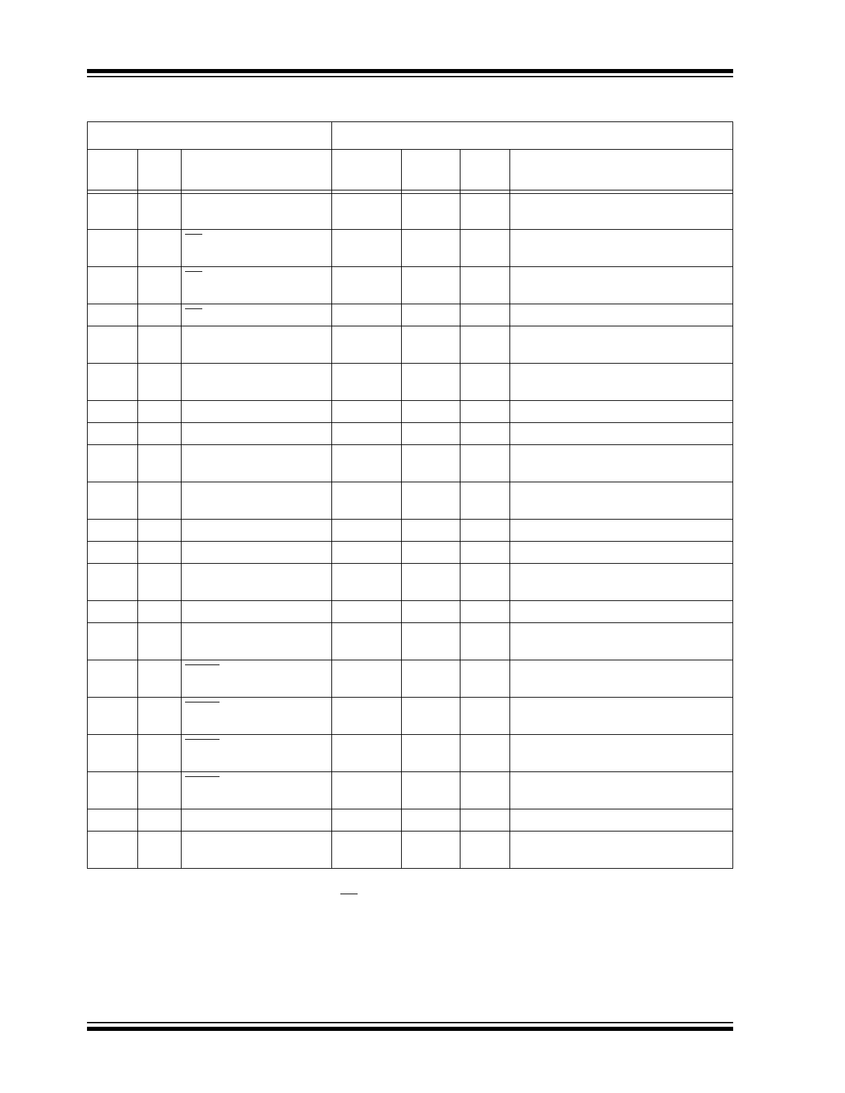
TABLE 1-2:
AC CHARACTERISTICS
AC CHARACTERISTICS
Extended (H):
T
A
= -40°C to +150°C
V
CC
= 2.5V to 5.5V
Param.
No.
Sym.
Characteristic
Min.
Max.
Units
Test Conditions
1
F
CLK
Clock Frequency
—
—
5
3
MHz
MHz
4.5V
≤ Vcc ≤ 5.5V
2.5V
≤ Vcc < 4.5V
2
T
CSS
CS Setup Time
100
150
—
—
ns
ns
4.5V
≤ Vcc ≤ 5.5V
2.5V
≤ Vcc < 4.5V
3
T
CSH
CS Hold Time
200
250
—
—
ns
ns
4.5V
≤ Vcc ≤ 5.5V
2.5V
≤ Vcc < 4.5V
4
T
CSD
CS Disable Time
50
—
ns
—
5
Tsu
Data Setup Time
20
30
—
—
ns
ns
4.5V
≤ Vcc ≤ 5.5V
2.5V
≤ Vcc < 4.5V
6
T
HD
Data Hold Time
40
50
—
—
ns
ns
4.5V
≤ Vcc ≤ 5.5V
2.5V
≤ Vcc < 4.5V
7
T
R
CLK Rise Time
—
100
ns
(Note 1)
8
T
F
CLK Fall Time
—
100
ns
(Note 1)
9
T
HI
Clock High Time
100
150
—
—
ns
ns
4.5V
≤ Vcc ≤ 5.5V
2.5V
≤ Vcc < 4.5V
10
T
LO
Clock Low Time
100
150
—
—
ns
ns
4.5V
≤ Vcc ≤ 5.5V
2.5V
≤ Vcc < 4.5V
11
T
CLD
Clock Delay Time
50
—
ns
—
12
T
CLE
Clock Enable Time
50
—
ns
—
13
T
V
Output Valid from Clock
Low
—
—
100
160
ns
ns
4.5V
≤ Vcc ≤ 5.5V
2.5V
≤ Vcc < 4.5V
14
T
HO
Output Hold Time
0
—
ns
(Note 1)
15
T
DIS
Output Disable Time
—
—
80
160
ns
ns
4.5V
≤ Vcc ≤ 5.5V (Note 1)
2.5V
≤ Vcc ≤ 4.5V (Note 1)
16
T
HS
HOLD Setup Time
40
80
—
—
ns
ns
4.5V
≤ Vcc ≤ 5.5V
2.5V
≤ Vcc < 4.5V
17
T
HH
HOLD Hold Time
40
80
—
—
ns
ns
4.5V
≤ Vcc ≤ 5.5V
2.5V
≤ Vcc < 4.5V
18
T
HZ
HOLD Low to Output
High-Z
60
160
—
—
ns
ns
4.5V
≤ Vcc ≤ 5.5V (Note 1)
2.5V
≤ Vcc < 4.5V (Note 1)
19
T
HV
HOLD High to Output
Valid
60
160
—
—
ns
ns
4.5V
≤ Vcc ≤ 5.5V
2.5V
≤ Vcc < 4.5V
20
T
WC
Internal Write Cycle Time
—
6
ms
(Note 2)
21
—
Endurance
1,000,000
—
E/W
Cycles
Page Mode, 25°C, V
CC
= 5.5V
(Note 3)
Note 1: This parameter is periodically sampled and not 100% tested.
2: T
WC
begins on the rising edge of CS after a valid write sequence and ends when the internal write cycle
is complete.
3: This parameter is not tested but ensured by characterization. For endurance estimates in a specific
application, please consult the Total Endurance™ Model which can be obtained from our web site:
www.microchip.com.
© 2009 Microchip Technology Inc.
Preliminary
DS22136B-page 5
25LCXXXA
TABLE 1-3:
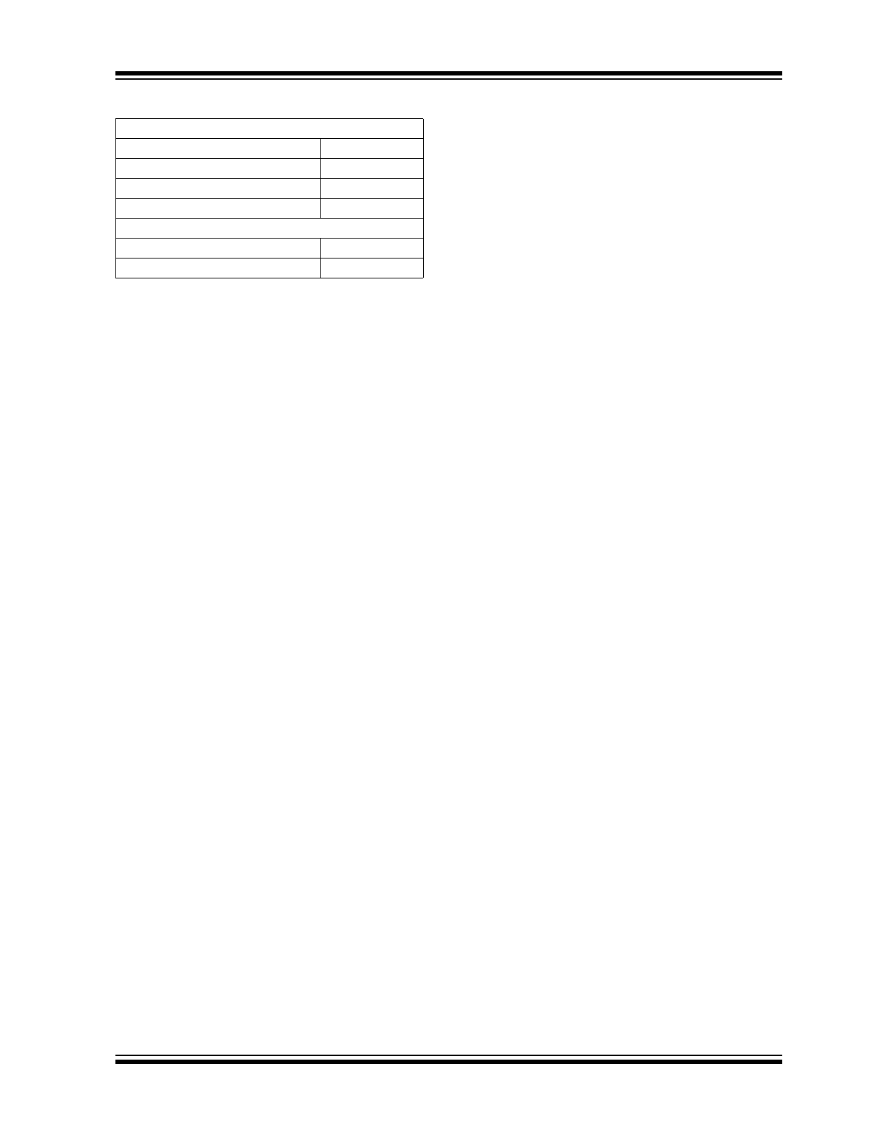
AC TEST CONDITIONS
AC Waveform:
V
LO
= 0.2V
—
V
H I
= V
CC
- 0.2V
(Note 1)
V
H I
= 4.0V
(Note 2)
C
L
= 50 pF
—
Timing Measurement Reference Level
Input
0.5 V
CC
Output
0.5 V
CC
Note 1: For V
CC
≤ 4.0V
2: For V
CC
> 4.0V
25LCXXXA
DS22136B-page 6
Preliminary
© 2009 Microchip Technology Inc.
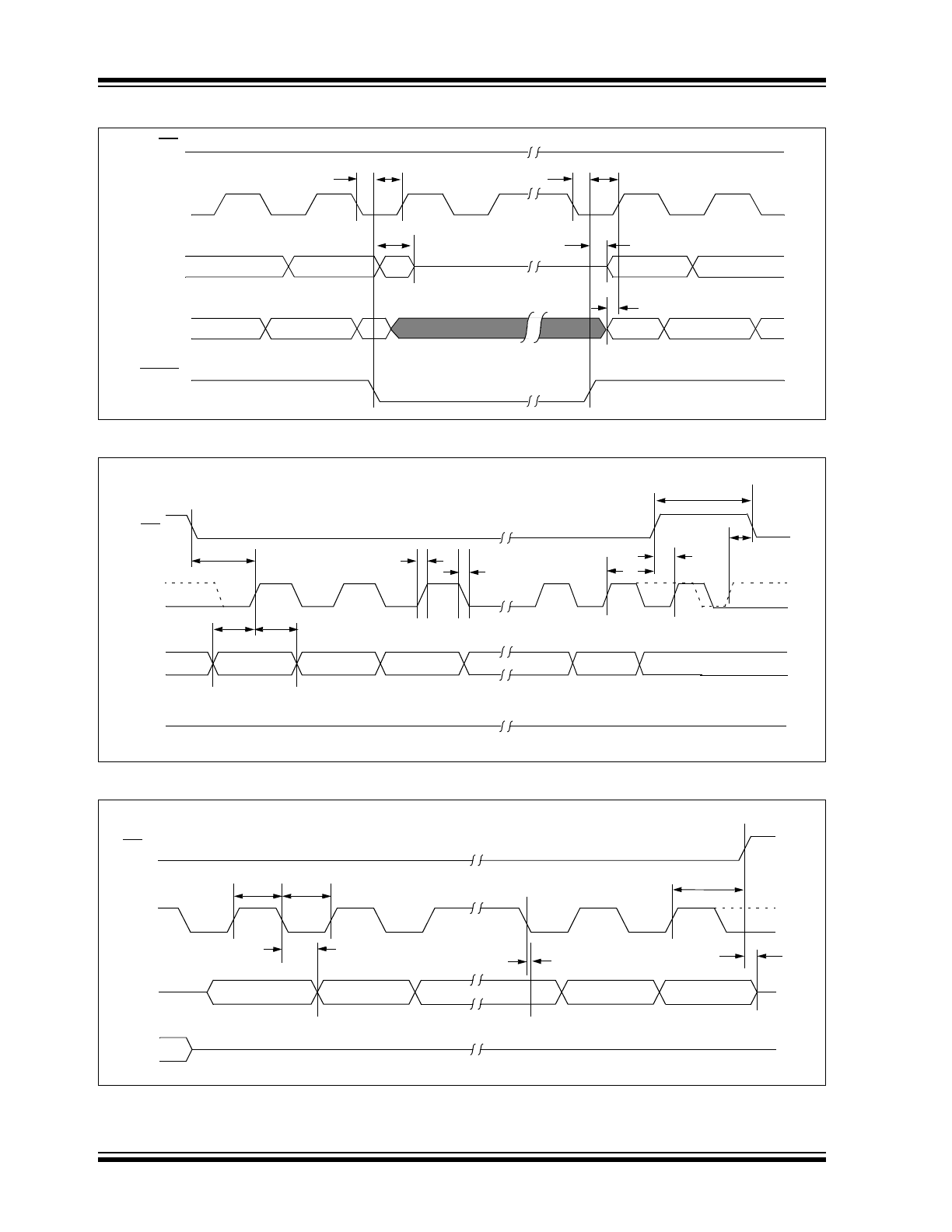
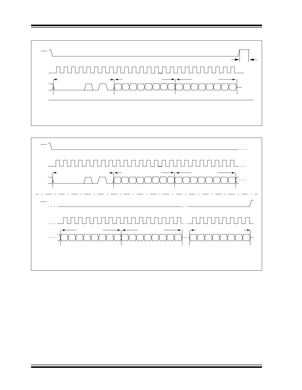
FIGURE 1-1:
HOLD TIMING
FIGURE 1-2:
SERIAL INPUT TIMING
FIGURE 1-3:
SERIAL OUTPUT TIMING
CS
SCK
SO
SI
HOLD
17
16
16
17
19
18
Don’t Care
5
High-Impedance
n + 2
n + 1
n
n - 1
n
n + 2
n + 1
n
n
n - 1
CS
SCK
SI
SO
6
5
8
7
11
3
LSB in
MSB in
High-Impedance
12
Mode 1,1
Mode 0,0
2
4
CS
SCK
SO
10
9
13
MSB out
ISB out
3
15
Don’t Care
SI
Mode 1,1
Mode 0,0
14
© 2009 Microchip Technology Inc.
Preliminary
DS22136B-page 7
25LCXXXA
2.0
PIN DESCRIPTIONS
The descriptions of the pins are listed in Table 2-1.
TABLE 2-1:
PIN FUNCTION TABLE
2.1
Chip Select (CS)
A low level on this pin selects the device. A high level
deselects the device and forces it into Standby mode.
However, a programming cycle which is already
initiated or in progress will be completed, regardless of
the CS input signal. If CS is brought high during a
program cycle, the device will go into Standby mode as
soon as the programming cycle is complete. When the
device is deselected, SO goes to the high-impedance
state, allowing multiple parts to share the same SPI
bus. A low-to-high transition on CS after a valid write
sequence initiates an internal write cycle. After power-
up, a low level on CS is required prior to any sequence
being initiated.
2.2
Serial Output (SO)
The SO pin is used to transfer data out of the
25LCXXXA. During a read cycle, data is shifted out on
this pin after the falling edge of the serial clock.
2.3
Write-Protect (WP)
The WP pin is a hardware write-protect input pin. When
it is low, all write to the array or STATUS registers are
disabled, but any other operations function normally.
When WP is high, all functions including nonvolatile
writes, operate normally. At any time, when WP is low,
the write enable Reset latch will be reset and program-
ming will be inhibited. However, if a write cycle is
already in progress, WP going low will not change or
disable the write cycle. See Table 5-1 for Write-Protect
Functionality Matrix.
2.4
Serial Input (SI)
The SI pin is used to transfer data into the device. It
receives instructions, addresses and data. Data is
latched on the rising edge of the serial clock.
2.5
Serial Clock (SCK)
The SCK is used to synchronize the communication
between a master and the 25LCXXXA. Instructions,
addresses or data present on the SI pin are latched on
the rising edge of the clock input, while data on the SO
pin is updated after the falling edge of the clock input.
2.6
Hold (HOLD)
The HOLD pin is used to suspend transmission to the
25LCXXXA while in the middle of a serial sequence
without having to retransmit the entire sequence again.
It must be held high any time this function is not being
used. Once the device is selected and a serial
sequence is underway, the HOLD pin may be pulled
low to pause further serial communication without
resetting the serial sequence. The HOLD pin must be
brought low while SCK is low, otherwise the HOLD
function will not be invoked until the next SCK high-to-
low transition. The 25LCXXXA must remain selected
during this sequence. The SI, SCK and SO pins are in
a high-impedance state during the time the device is
paused and transitions on these pins will be ignored. To
resume serial communication, HOLD must be brought
high while the SCK pin is low, otherwise serial
communication will not resume. Lowering the HOLD
line at any time will tri-state the SO line.
Name
Pin Number
Function
CS
1
Chip Select Input
SO
2
Serial Data Output
WP
3
Write-Protect Pin
V
SS
4
Ground
SI
5
Serial Data Input
SCK
6
Serial Clock Input
HOLD
7
Hold Input
V
CC
8
Supply Voltage
25LCXXXA
DS22136B-page 8
Preliminary
© 2009 Microchip Technology Inc.
3.0
FUNCTIONAL DESCRIPTION
3.1
Principles of Operation
The 25LCXXXA are low-density serial EEPROMs
designed to interface directly with the Serial Peripheral
Interface (SPI) port of many of today’s popular micro-
controller families, including Microchip’s PIC
®
micro-
controllers. It may also interface with microcontrollers
that do not have a built-in SPI port by using discrete I/
O lines programmed properly in firmware to match the
SPI protocol.
The 25LCXXXA contains an 8-bit instruction register.
The device is accessed via the SI pin, with data being
clocked in on the rising edge of SCK. The CS pin must
be low and the HOLD pin must be high for the entire
operation.
Table 3-1 contains a list of the possible instruction
bytes and format for device operation. All instructions,
addresses, and data are transferred MSB first, LSB
last.
Data (SI) is sampled on the first rising edge of SCK
after CS goes low. If the clock line is shared with other
peripheral devices on the SPI bus, the user can assert
the HOLD input and place the 25LCXXXA in ‘HOLD’
mode. After releasing the HOLD pin, operation will
resume from the point when the HOLD was asserted.
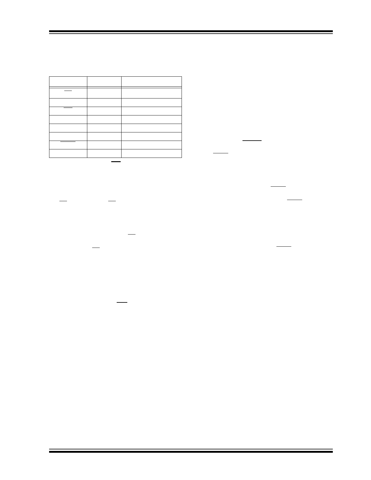
BLOCK DIAGRAM
TABLE 3-1:
INSTRUCTION SET
SI
SO
SCK
CS
HOLD
WP
STATUS
Register
I/O Control
Memory
Control
Logic
X
Dec
HV Generator
EEPROM
Array
Page Latches
Y Decoder
Sense Amp.
R/W Control
Logic
V
CC
V
SS
Instruction Name
Instruction Format
Description
READ
0000 A
8
011
Read data from memory array beginning at selected address
WRITE
0000 A
8
010
Write data to memory array beginning at selected address
WRDI
0000 x100
Reset the write enable latch (disable write operations)
WREN
0000 x110
Set the write enable latch (enable write operations)
RDSR
0000 x101
Read STATUS register
WRSR
0000 x001
Write STATUS register
Note:
For the 24LC040A device, A
8
is the 9
th
address bit, which is used to address the entire 512 byte array.
For the 24LC020A and 24LC010A devcies, A
8
is a don’t care.
x
= don’t care.
© 2009 Microchip Technology Inc.
Preliminary
DS22136B-page 9
25LCXXXA
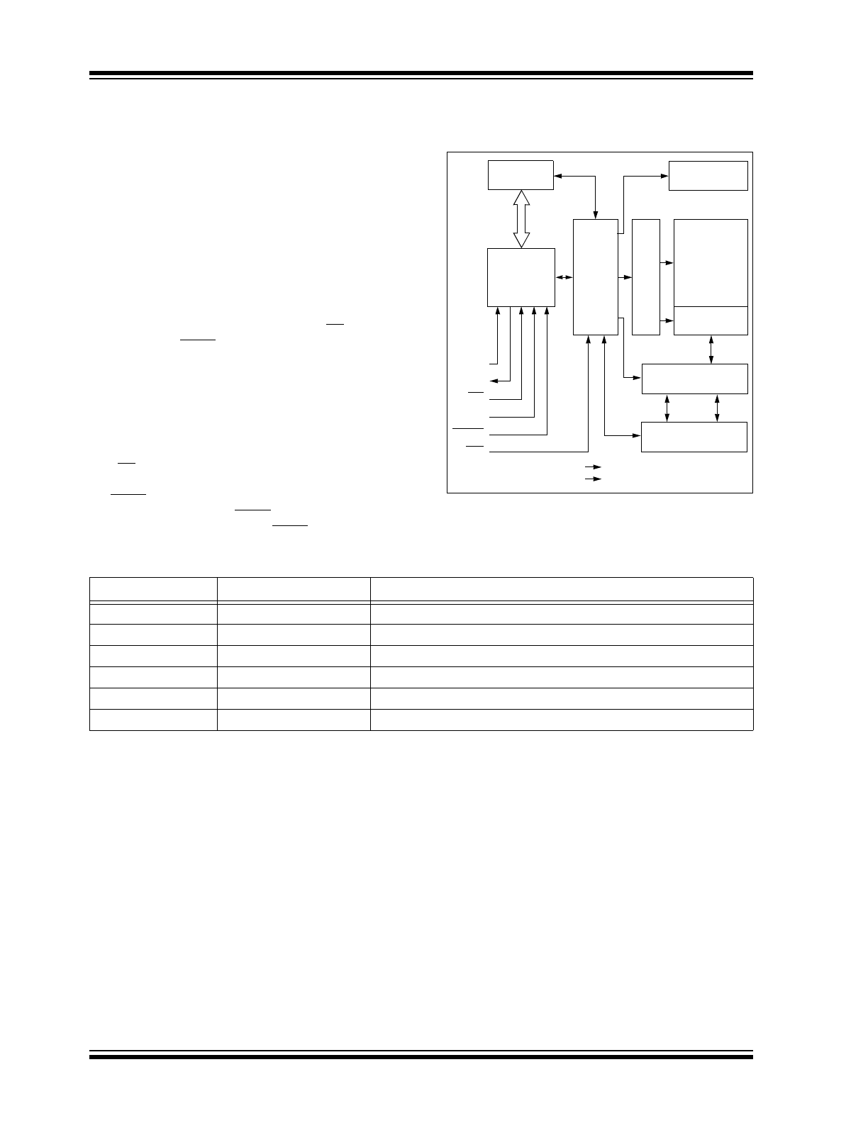
3.2
Read Sequence
The device is selected by pulling CS low. The 8-bit
READ
instruction is transmitted to the 25LCXXXA fol-
lowed by the 8-bit address. For the 25LC040A the MSb
(A8) is sent to the slave during the instruction
sequence. See Figure 3-1 for more details. After the
correct READ instruction and address are sent, the data
stored in the memory at the selected address is shifted
out on the SO pin. The data stored in the memory at the
next address can be read sequentially by continuing to
provide clock pulses. The internal Address Pointer is
automatically incremented to the next higher address
after each byte of data is shifted out. When the highest
address is reached, the address counter rolls over to
address 000h allowing the read cycle to be continued
indefinitely. The read operation is terminated by raising
the CS pin (Figure 3-1).
3.3
Write Sequence
Prior to any attempt to write data to the 25LCXXXA, the
write enable latch must be set by issuing the WREN
instruction (Figure 3-4). This is done by setting CS low
and then clocking out the proper instruction into the
25LCXXXA. After all eight bits of the instruction are
transmitted, the CS must be brought high to set the
write enable latch. If the write operation is initiated
immediately after the WREN instruction without CS
being brought high, the data will not be written to the
array because the write enable latch will not have been
properly set.
Once the write enable latch is set, the user may
proceed by setting the CS low, issuing a WRITE instruc-
tion, followed by the 8-bit address, and then the data to
be written. Up to 16 bytes can be sent to the device
before a write cycle is necessary. The only restriction is
that all of the bytes must reside in the same page. Addi-
tionally a page address begins with ‘XXXX 0000’ and
ends with ‘XXXX 1111’. If the internal address counter
reaches ‘XXXX 1111’ and clock signals continue to be
applied to the ship, the address counter will roll back to
the first address of the page and over-write any data
that previously existed in those locations.
For the data to be actually written to the array, the CS
must be brought high after the Least Significant bit (D0)
of the n
th
data byte has been clocked in. If CS is
brought high at any other time, the write operation will
not be completed. Refer to Figure 3-6 and Figure 3-4
for more detailed illustrations on the byte write
sequence and the page write sequence, respectively.
While the write is in progress, the STATUS register may
be read to check the status of the WIP, WEL, BP1 and
BP0 bits (Figure 3-6). A read attempt of a memory
array location will not be possible during a write cycle.
When the write cycle is completed, the write enable
latch is reset.
FIGURE 3-1:
READ SEQUENCE
Note:
Page write operations are limited to writing
bytes within a single physical page,
regardless of the number of bytes
actually being written. Physical page
boundaries start at addresses that are
integer multiples of the page buffer size (or
‘page size’) and, end at addresses that are
integer multiples of page size – 1. If a page
write command attempts to write across a
physical page boundary, the result is that
the data wraps around to the beginning of
the current page (overwriting data
previously stored there), instead of being
written to the next page as might be
expected. It is therefore necessary for the
application software to prevent page write
operations that would attempt to cross a
page boundary.
SO
SI
SCK
CS
0
2
3
4
5
6
7
8
9 10 11
1
0
1
A
8
0
0
0
0
1
A
7
A
6
A
5
A
4
A
1
A
0
7
6
5
4
3
2
1
0
Data Out
High-impedance
A
3
A
2
Lower Address Byte
12 13 14 15 16 17 18 19 20 21 22 23
Instruction+Address MSb
For the 24LC010A device both A8 and A7 are don’t cares.
For the 24LC020A device A8 is a don’t care.
25LCXXXA
DS22136B-page 10
Preliminary
© 2009 Microchip Technology Inc.
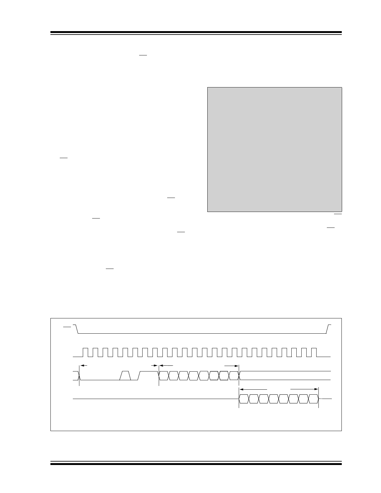
FIGURE 3-2:
BYTE WRITE SEQUENCE
FIGURE 3-3:
PAGE WRITE SEQUENCE
SI
CS
9 10 11
0
0
A
8
0
0
0
0
1
7
6
5
4
3
2
1
0
Data Byte
SCK
0
2
3
4
5
6
7
1
8
Instruction+Address MSb
Lower Address Byte
A
7
A
6
A
5
A
4
A
3
A
1
A
0
A
2
12 13 14 15 16 17 18 19 20 21 22 23
Twc
SO
High-impedance
For the 24LC010A device both A8 and A7 are don’t cares.
For the 24LC020A device A8 is a don’t care.
SI
CS
9 10 11
0
0
A
8
0
0
0
0
1
7
6
5
4
3
2
1
0
Data Byte 1
SCK
0
2
3
4
5
6
7
1
8
SI
CS
33 34 35
38 39
7
6
5
4
3
2
1
0
Data Byte n (16 max.)
SCK
24
26 27 28 29 30 31
25
32
7
6
5
4
3
2
1
0
Data Byte 3
7
6
5
4
3
2
1
0
Data Byte 2
36 37
Instruction+Address MSb
Lower Address Byte
A
7
A
6
A
5
A
4
A
3
A
1
A
0
A
2
12 13 14 15 16 17 18 19 20 21 22 23
For the 24LC010A device both A8 and A7 are don’t cares.
For the 24LC020A device A8 is a don’t care.