

A Microchip Technology Company
©2011 Silicon Storage Technology, Inc.
DS25080A
11/11
Not Recommended for New Designs
www.microchip.com
Features
• Single 3.0-3.6V Read and Write Operations
• Serial Interface Architecture
– SPI Compatible: Mode 0 and Mode 3
• 33 MHz Max Clock Frequency
• Superior Reliability
– Endurance: 100,000 Cycles (typical)
– Greater than 100 years Data Retention
• Low Power Consumption:
– Active Read Current: 7 mA (typical)
– Standby Current: 8 µA (typical)
• Flexible Erase Capability
– Uniform 4 KByte sectors
– Uniform 32 KByte overlay blocks
• Fast Erase and Byte-Program:
– Chip-Erase Time: 70 ms (typical)
– Sector- or Block-Erase Time: 18 ms (typical)
– Byte-Program Time: 14 µs (typical)
• Auto Address Increment (AAI) Programming
– Decrease total chip programming time over Byte-Pro-
gram operations
• End-of-Write Detection
– Software Status
• Hold Pin (HOLD#)
– Suspends a serial sequence to the memory
without deselecting the device
• Write Protection (WP#)
– Enables/Disables the Lock-Down function of the status
register
• Software Write Protection
– Write protection through Block-Protection bits in status
register
• Temperature Range
– Commercial: 0°C to +70°C
– Industrial: -40°C to +85°C
– Extended: -20°C to +85°C
• Packages Available
– 8-lead SOIC 150 mil body width
for SST25LF020A
– 8-contact WSON (5mm x 6mm)
• All non-Pb (lead-free) devices are RoHS compliant
2 Mbit SPI Serial Flash
SST25LF020A
SST serial flash family features a four-wire, SPI-compatible interface that allows
for a low pin-count package occupying less board space and ultimately lowering
total system costs. SST25LF020A SPI serial flash memory is manufactured with
SST proprietary, high performance CMOS SuperFlash Technology. The split-gate
cell design and thick-oxide tunneling injector attain better reliability and manufac-
turability compared with alternate approaches.
Not recommended for new designs.
Please use SST25VF020B

©2011 Silicon Storage Technology, Inc.
DS25080A
11/11
2
2 Mbit SPI Serial Flash
SST25LF020A
Not Recommended for New Designs
A Microchip Technology Company
Product Description
SST’s serial flash family features a four-wire, SPI-compatible interface that allows for a low pin-
count package occupying less board space and ultimately lowering total system costs.
SST25LF020A SPI serial flash memories are manufactured with SST’s proprietary, high perfor-
mance CMOS SuperFlash technology. The split-gate cell design and thick-oxide tunneling injector
attain better reliability and manufacturability compared with alternate approaches.
The SST25LF020A devices significantly improve performance, while lowering power consumption.
The total energy consumed is a function of the applied voltage, current, and time of application.
Since for any given voltage range, the SuperFlash technology uses less current to program and
has a shorter erase time, the total energy consumed during any Erase or Program operation is
less than alternative flash memory technologies. The SST25LF020A devices operate with a single
3.0-3.6V power supply.
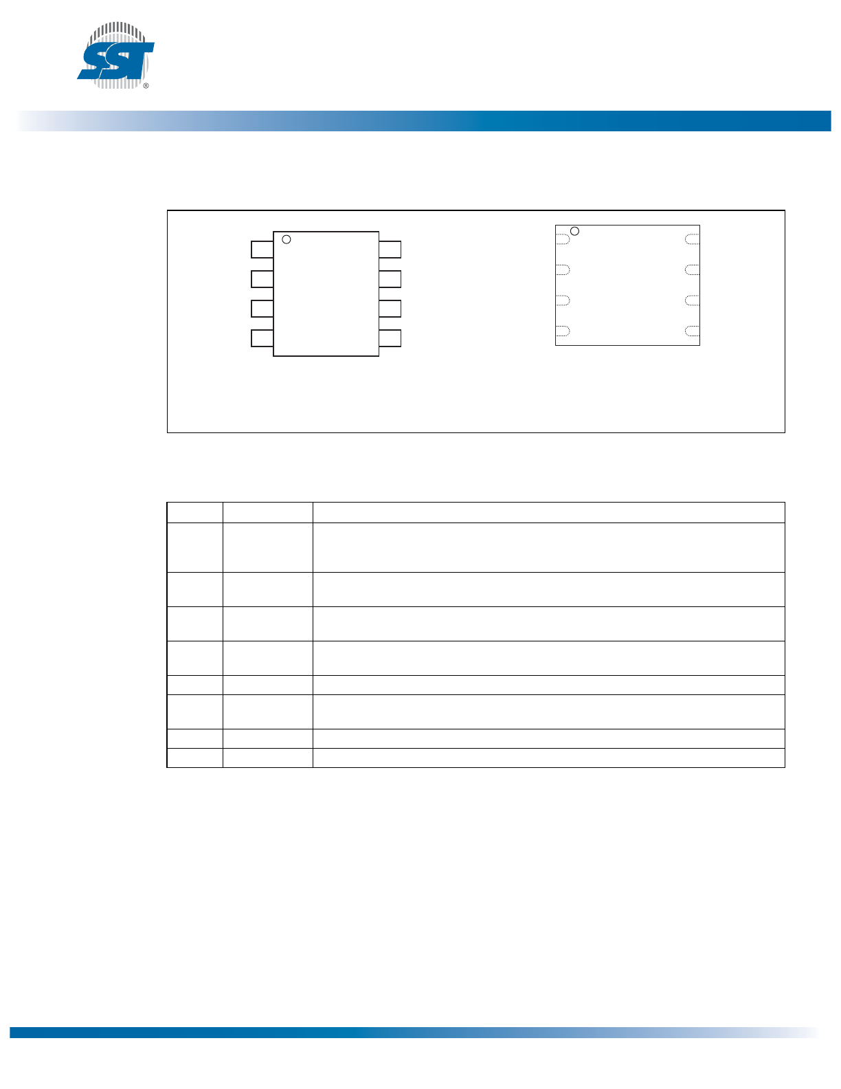
The SST25LF020A devices are offered in an 8-lead SOIC 150 mil body width (SA) package, and in
an 8-contact WSON package. See Figure 2 for the pin assignments.
©2011 Silicon Storage Technology, Inc.
DS25080A
11/11
3
2 Mbit SPI Serial Flash
SST25LF020A
Not Recommended for New Designs
A Microchip Technology Company
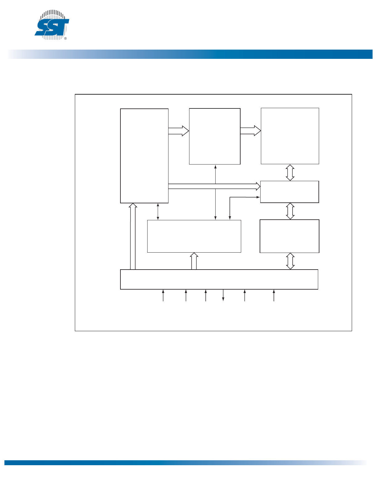
Block Diagram
Figure 1: Functional Block Diagram
1242 B1.0
I/O Buffers
and
Data Latches
SuperFlash
Memory
X - Decoder
Control Logic
Address
Buffers
and
Latches
CE#
Y - Decoder
SCK
SI
SO
WP#
HOLD#
Serial Interface
©2011 Silicon Storage Technology, Inc.
DS25080A
11/11
4
2 Mbit SPI Serial Flash
SST25LF020A
Not Recommended for New Designs
A Microchip Technology Company
Pin Description
Figure 2: Pin Assignments
Table 1: Pin Description
Symbol
Pin Name
Functions
SCK
Serial Clock
To provide the timing of the serial interface.
Commands, addresses, or input data are latched on the rising edge of the clock input,
while output data is shifted out on the falling edge of the clock input.
SI
Serial Data
Input
To transfer commands, addresses, or data serially into the device.
Inputs are latched on the rising edge of the serial clock.
SO
Serial Data
Output
To transfer data serially out of the device.
Data is shifted out on the falling edge of the serial clock.
CE#
Chip Enable
The device is enabled by a high to low transition on CE#. CE# must remain low for the
duration of any command sequence.
WP#
Write Protect
The Write Protect (WP#) pin is used to enable/disable BPL bit in the status register.
HOLD#
Hold
To temporarily stop serial communication with SPI flash memory without resetting the
device.
V
DD
Power Supply
To provide power supply (3.0-3.6V).
V
SS
Ground
T1.0 25080
8-lead SOIC
8-contact WSON
1
2
3
4
8
7
6
5
CE#
SO
WP#
VSS
Top View
VDD
HOLD#
SCK
SI
1242 08-wson P2.0
1
2
3
4
8
7
6
5
CE#
SO
WP#
VSS
VDD
HOLD#
SCK
SI
Top View
1242 08-soic P1.0
©2011 Silicon Storage Technology, Inc.
DS25080A
11/11
5
2 Mbit SPI Serial Flash
SST25LF020A
Not Recommended for New Designs
A Microchip Technology Company
Memory Organization
The SST25LF020A SuperFlash memory array is organized in 4 KByte sectors with 32 KByte overlay
blocks.
Device Operation
The SST25LF020A is accessed through the SPI (Serial Peripheral Interface) bus compatible protocol.
The SPI bus consist of four control lines; Chip Enable (CE#) is used to select the device, and data is
accessed through the Serial Data Input (SI), Serial Data Output (SO), and Serial Clock (SCK).
The SST25LF020A supports both Mode 0 (0,0) and Mode 3 (1,1) of SPI bus operations. The differ-
ence between the two modes, as shown in Figure 3, is the state of the SCK signal when the bus mas-
ter is in Stand-by mode and no data is being transferred. The SCK signal is low for Mode 0 and SCK
signal is high for Mode 3. For both modes, the Serial Data In (SI) is sampled at the rising edge of the
SCK clock signal and the Serial Data Output (SO) is driven after the falling edge of the SCK clock sig-
nal.
Figure 3: SPI Protocol
1242 F02.0
MODE 3
SCK
SI
SO
CE#
MODE 3
DON T CARE
Bit 7 Bit 6 Bit 5 Bit 4 Bit 3 Bit 2 Bit 1 Bit 0
Bit 7 Bit 6 Bit 5 Bit 4 Bit 3 Bit 2 Bit 1Bit 0
MODE 0
MODE 0
HIGH IMPEDANCE
MSB
MSB
©2011 Silicon Storage Technology, Inc.
DS25080A
11/11
6
2 Mbit SPI Serial Flash
SST25LF020A
Not Recommended for New Designs
A Microchip Technology Company
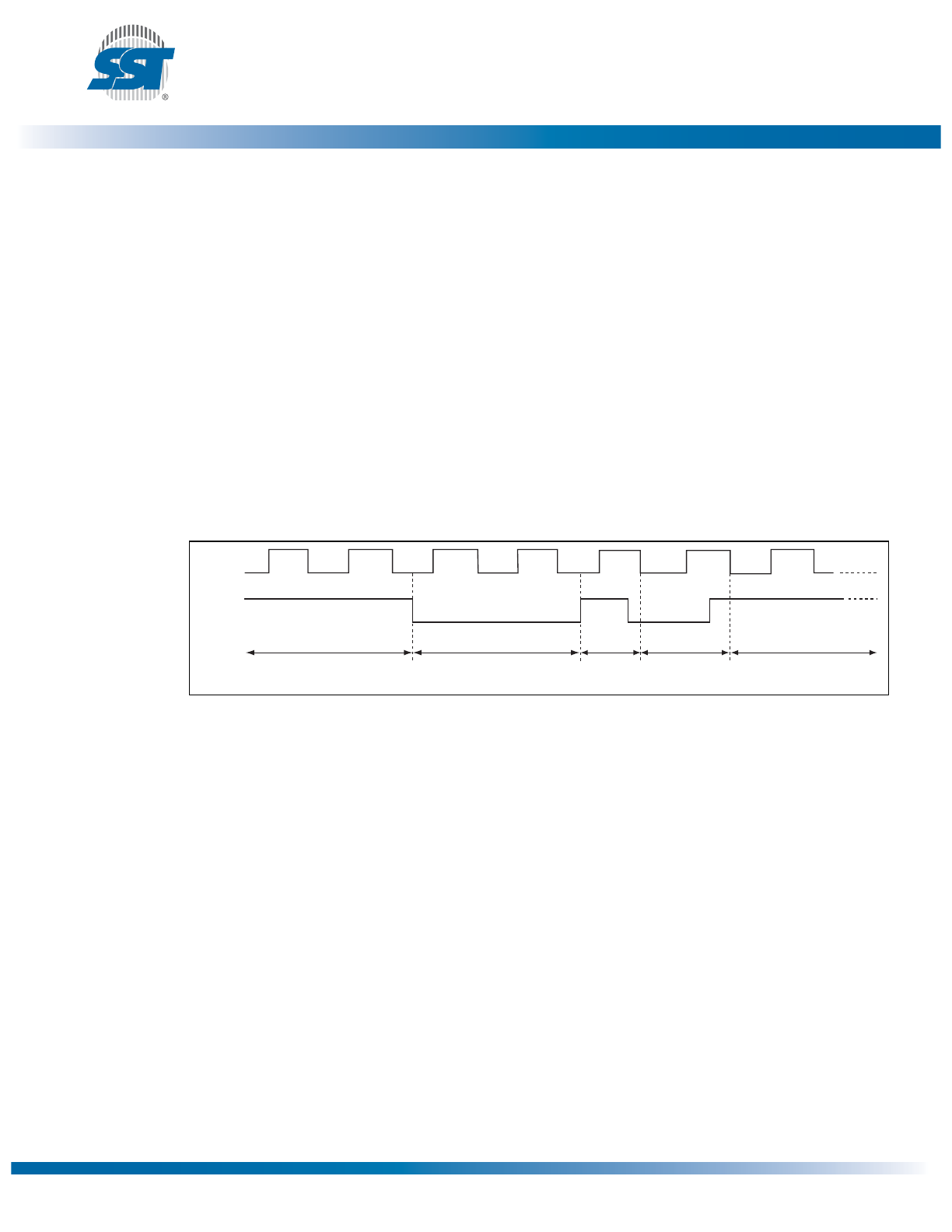
Hold Operation
HOLD# pin is used to pause a serial sequence underway with the SPI flash memory without resetting
the clocking sequence. To activate the HOLD# mode, CE# must be in active low state. The HOLD#
mode begins when the SCK active low state coincides with the falling edge of the HOLD# signal. The
HOLD mode ends when the HOLD# signal’s rising edge coincides with the SCK active low state.
If the falling edge of the HOLD# signal does not coincide with the SCK active low state, then the device
enters Hold mode when the SCK next reaches the active low state. Similarly, if the rising edge of the
HOLD# signal does not coincide with the SCK active low state, then the device exits in Hold mode
when the SCK next reaches the active low state. See Figure 4 for Hold Condition waveform.
Once the device enters Hold mode, SO will be in high-impedance state while SI and SCK can be V
IL
or
V
IH
.
If CE# is driven active high during a Hold condition, it resets the internal logic of the device. As long as
HOLD# signal is low, the memory remains in the Hold condition. To resume communication with the
device, HOLD# must be driven active high, and CE# must be driven active low. See Figure 19 for Hold
timing.
Figure 4: Hold Condition Waveform
Write Protection
SST25LF020A provides software Write protection. The Write Protect pin (WP#) enables or disables
the lock-down function of the status register. The Block-Protection bits (BP1, BP0, and BPL) in the sta-
tus register provide Write protection to the memory array and the status register. See Table 4 for Block-
Protection description.
Active
Hold
Active
Hold
Active
1242 F03.0
SCK
HOLD#
©2011 Silicon Storage Technology, Inc.
DS25080A
11/11
7
2 Mbit SPI Serial Flash
SST25LF020A
Not Recommended for New Designs
A Microchip Technology Company
Write Protect Pin (WP#)
The Write Protect (WP#) pin enables the lock-down function of the BPL bit (bit 7) in the status register.
When WP# is driven low, the execution of the Write-Status-Register (WRSR) instruction is determined
by the value of the BPL bit (see Table 2). When WP# is high, the lock-down function of the BPL bit is
disabled.
Status Register
The software status register provides status on whether the flash memory array is available for any
Read or Write operation, whether the device is Write enabled, and the state of the memory Write pro-
tection. During an internal Erase or Program operation, the status register may be read only to deter-
mine the completion of an operation in progress. Table 3 describes the function of each bit in the
software status register.
Busy
The Busy bit determines whether there is an internal Erase or Program operation in progress. A “1” for
the Busy bit indicates the device is busy with an operation in progress. A “0” indicates the device is
ready for the next valid operation.
Table 2: Conditions to execute Write-Status-Register (WRSR) Instruction
WP#
BPL
Execute WRSR Instruction
L
1
Not Allowed
L
0
Allowed
H
X
Allowed
T2.0 25080
Table 3: Software Status Register
Bit
Name
Function
Default at
Power-up
Read/Write
0
BUSY
1 = Internal Write operation is in progress
0 = No internal Write operation is in progress
0
R
1
WEL
1 = Device is memory Write enabled
0 = Device is not memory Write enabled
0
R
2
BP0
Indicate current level of block write protection (See
Table 4)
1
R/W
3
BP1
Indicate current level of block write protection (See
Table 4)
1
R/W
4:5
RES
Reserved for future use
0
N/A
6
AAI
Auto Address Increment Programming status
1 = AAI programming mode
0 = Byte-Program mode
0
R
7
BPL
1 = BP1, BP0 are read-only bits
0 = BP1, BP0 are read/writable
0
R/W
T3.0 25080
©2011 Silicon Storage Technology, Inc.
DS25080A
11/11
8
2 Mbit SPI Serial Flash
SST25LF020A
Not Recommended for New Designs
A Microchip Technology Company
Write Enable Latch (WEL)
The Write-Enable-Latch bit indicates the status of the internal memory Write Enable Latch. If the
Write-Enable-Latch bit is set to “1”, it indicates the device is Write enabled. If the bit is set to “0” (reset),
it indicates the device is not Write enabled and does not accept any memory Write (Program/Erase)
commands. The Write-Enable-Latch bit is automatically reset under the following conditions:
•
Power-up
•
Write-Disable (WRDI) instruction completion
•
Byte-Program instruction completion
•
Auto Address Increment (AAI) programming reached its highest memory address
•
Sector-Erase instruction completion
•
Block-Erase instruction completion
•
Chip-Erase instruction completion
Block Protection (BP1, BP0)
The Block-Protection (BP1, BP0) bits define the size of the memory area, as defined in Table 4, to be
software protected against any memory Write (Program or Erase) operations. The Write-Status-Regis-
ter (WRSR) instruction is used to program the BP1 and BP0 bits as long as WP# is high or the Block-
Protect-Lock (BPL) bit is 0. Chip-Erase can only be executed if Block-Protection bits are both 0. After
power-up, BP1 and BP0 are set to 1.
Block Protection Lock-Down (BPL)
WP# pin driven low (V
IL
), enables the Block-Protection-Lock-Down (BPL) bit. When BPL is set to 1, it
prevents any further alteration of the BPL, BP1, and BP0 bits. When the WP# pin is driven high (V
IH
),
the BPL bit has no effect and its value is “Don’t Care”. After power-up, the BPL bit is reset to 0.
Auto Address Increment (AAI)
The Auto Address Increment Programming-Status bit provides status on whether the device is in AAI
programming mode or Byte-Program mode. The default at power up is Byte-Program mode.
Table 4: Software Status Register Block Protection
1
1. Default at power-up for BP1 and BP0 is ‘11’.
Protection Level
Status Register Bit
Protected Memory Area
BP1
BP0
2 Mbit
0
0
0
None
1 (1/4 Memory Array)
0
1
030000H-03FFFFH
2 (1/2 Memory Array)
1
0
020000H-03FFFFH
3 (Full Memory Array)
1
1
000000H-03FFFFH
T4.0 25080
©2011 Silicon Storage Technology, Inc.
DS25080A
11/11
9
2 Mbit SPI Serial Flash
SST25LF020A
Not Recommended for New Designs
A Microchip Technology Company
Instructions
Instructions are used to Read, Write (Erase and Program), and configure the SST25LF020A. The
instruction bus cycles are 8 bits each for commands (Op Code), data, and addresses. Prior to execut-
ing any Byte-Program, Auto Address Increment (AAI) programming, Sector-Erase, Block-Erase, or
Chip-Erase instructions, the Write-Enable (WREN) instruction must be executed first. The complete list
of the instructions is provided in Table 5. All instructions are synchronized off a high to low transition of
CE#. Inputs will be accepted on the rising edge of SCK starting with the most significant bit. CE# must
be driven low before an instruction is entered and must be driven high after the last bit of the instruction
has been shifted in (except for Read, Read-ID and Read-Status-Register instructions). Any low to high
transition on CE#, before receiving the last bit of an instruction bus cycle, will terminate the instruction
in progress and return the device to the standby mode. Instruction commands (Op Code), addresses,
and data are all input from the most significant bit (MSB) first.
Table 5: Device Operation Instructions
1
1. A
MS
= Most Significant Address
A
MS
= A
17
for SST25LF020A
Address bits above the most significant bit of each density can be V
IL
or V
IH
Cycle Type/
Operation
2,3
2. Operation: S
IN
= Serial In, S
OUT
= Serial Out
3. X = Dummy Input Cycles (V
IL
or V
IH
); - = Non-Applicable Cycles (Cycles are not necessary)
Max
Freq
MHz
Bus Cycle
4
4. One bus cycle is eight clock periods.
1
2
3
4
5
6
S
IN
S
OUT
S
IN
S
OUT
S
IN
S
OUT
S
IN
S
OUT
S
IN
S
OUT
S
IN
S
OUT
Read
20
03H
Hi-Z
A
23
-
A
16
Hi-Z
A
15
-
A
8
Hi-Z
A
7
-A
0
Hi-Z
X
D
OUT
High-Speed-Read
33
0BH
Hi-Z
A
23
-
A
16
Hi-Z
A
15
-
A
8
Hi-Z
A
7
-A
0
Hi-Z
X
X
X
D
OUT
Sector-Erase
5,6
5. Sector addresses: use A
MS
-A
12
, remaining addresses can be V
IL
or V
IH
6. Prior to any Byte-Program, AAI-Program, Sector-Erase, Block-Erase, or Chip-Erase operation, the Write-Enable
(WREN) instruction must be executed.
20H
Hi-Z
A
23
-
A
16
Hi-Z
A
15
-
A
8
Hi-Z
A
7
-A
0
Hi-Z
-
-
Block-Erase
5,7
52H
Hi-Z
A
23
-
A
16
Hi-Z
A
15
-
A
8
Hi-Z
A
7
-A
0
Hi-Z
-
-
Chip-Erase
6
60H
Hi-Z
-
-
-
-
-
-
-
-
Byte-Program
6
02H
Hi-Z
A
23
-
A
16
Hi-Z
A
15
-
A
8
Hi-Z
A
7
-A
0
Hi-Z
D
IN
Hi-Z
Auto Address Increment
(AAI) Single-Byte
Program
6,8
AFH
Hi-Z
A
23
-
A
16
Hi-Z
A
15
-
A
8
Hi-Z
A
7
-A
0
Hi-Z
D
IN
Hi-Z
Read-Status-Register
(RDSR)
05H
Hi-Z
X
D
OUT
-
Note
9
-
Note
9
-
Note
9
Enable-Write-Status-
Register
(EWSR)
10
50H
Hi-Z
-
-
-
-
-
-
-
-
Write-Status-Register
(WRSR)
10
01H
Hi-Z
Data
Hi-Z
-
-
-.
-
-
-
Write-Enable (WREN)
06H
Hi-Z
-
-
-
-
-
-
-
-
Write-Disable (WRDI)
04H
Hi-Z
-
-
-
-
-
-
-
-
Read-ID
90H
or
ABH
Hi-Z
00H
Hi-Z
00H
Hi-Z
ID
Addr
11
Hi-Z
X
D
OUT
12
T5.0 25080
©2011 Silicon Storage Technology, Inc.
DS25080A
11/11
10
2 Mbit SPI Serial Flash
SST25LF020A
Not Recommended for New Designs
A Microchip Technology Company
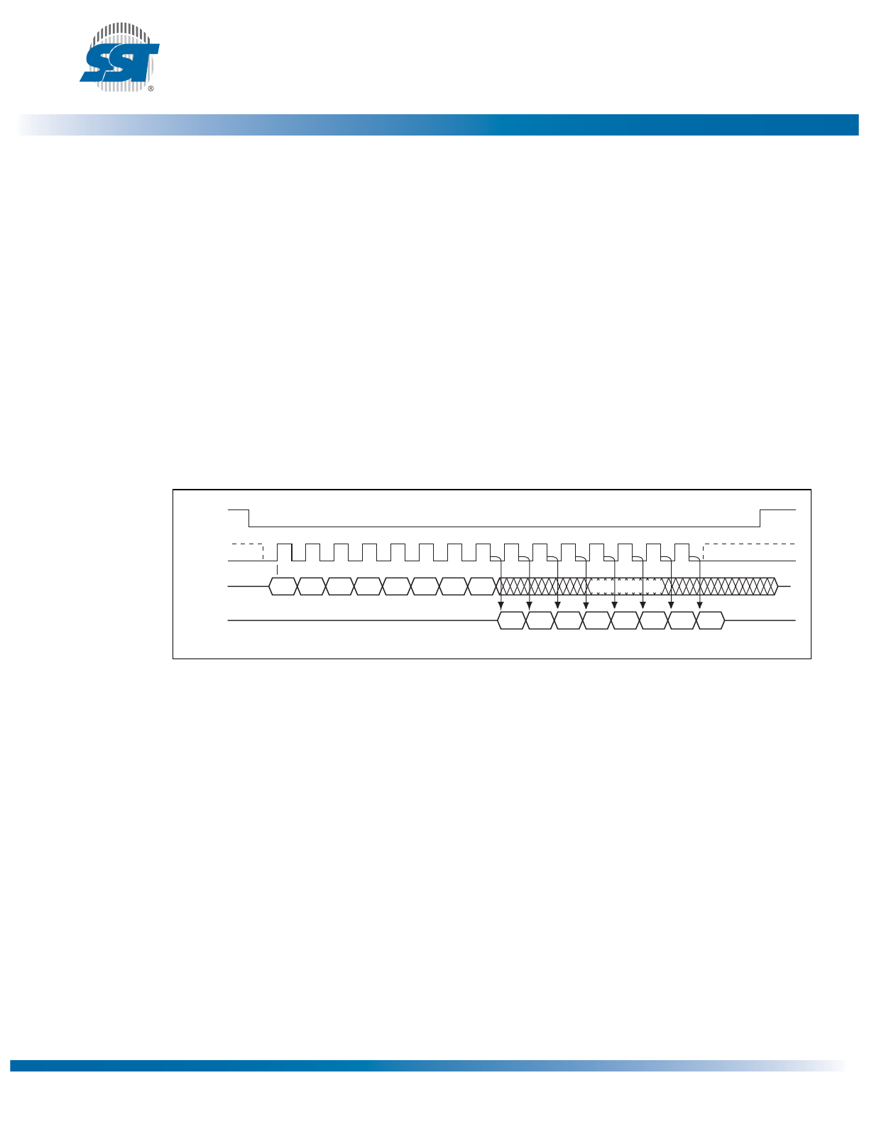
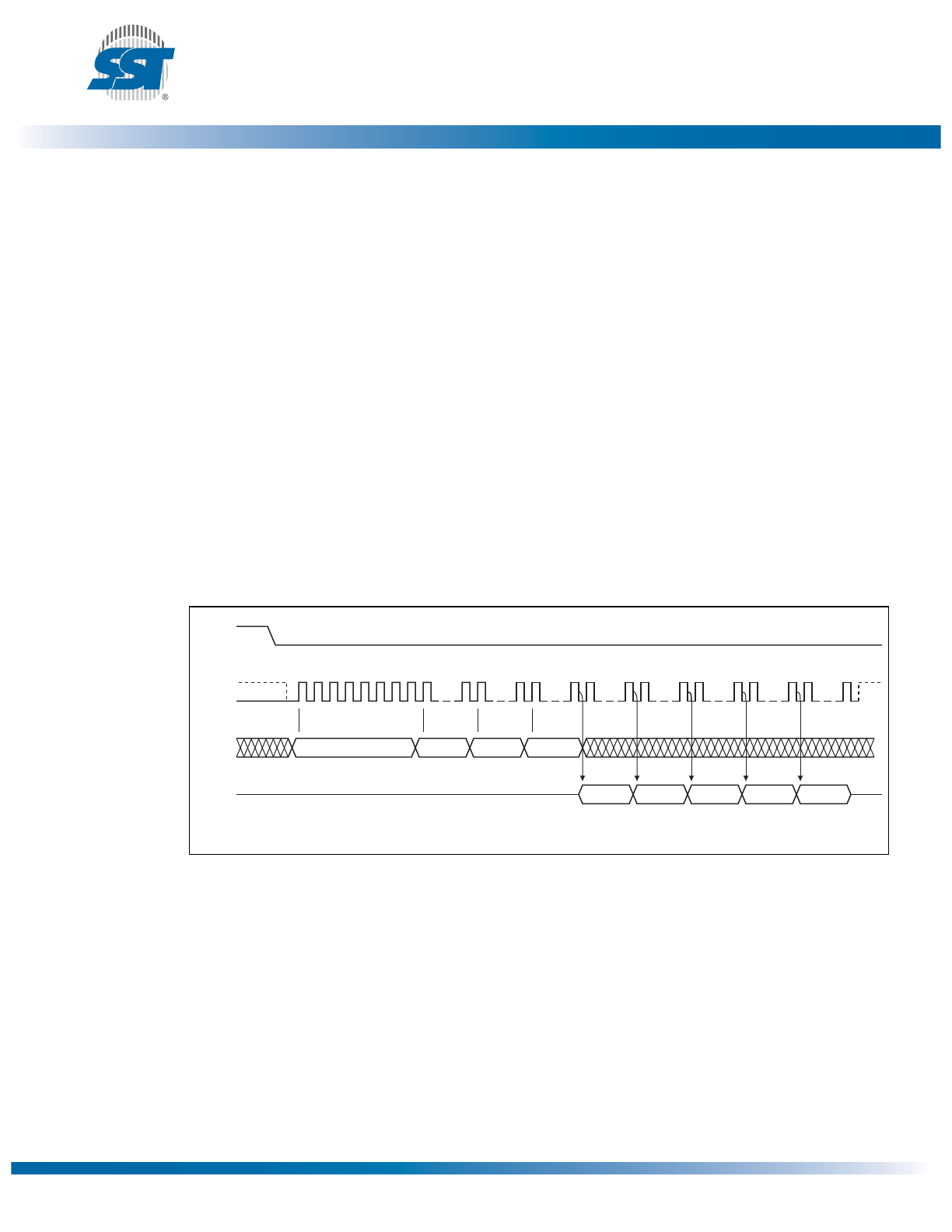
Read (20 MHz)
The Read instruction supports up to 20 MHz, it outputs the data starting from the specified address
location. The data output stream is continuous through all addresses until terminated by a low to high
transition on CE#. The internal address pointer will automatically increment until the highest memory
address is reached. Once the highest memory address is reached, the address pointer will automati-
cally increment to the beginning (wrap-around) of the address space, i.e. for 2 Mbit density, once the
data from address location 3FFFFH had been read, the next output will be from address location
00000H.
The Read instruction is initiated by executing an 8-bit command, 03H, followed by address bits [A
23
-
A
0
]. CE# must remain active low for the duration of the Read cycle. See Figure 5 for the Read
sequence.
Figure 5: Read Sequence
7. Block addresses for: use A
MS
-A
15
, remaining addresses can be V
IL
or V
IH
8. To continue programming to the next sequential address location, enter the 8-bit command, AFH,
followed by the data to be programmed.
9. The Read-Status-Register is continuous with ongoing clock cycles until terminated by a low to high transition on CE#.
10. The Enable-Write-Status-Register (EWSR) instruction and the Write-Status-Register (WRSR) instruction must work in
conjunction of each other. The WRSR instruction must be executed immediately (very next bus cycle) after the EWSR
instruction to make both instructions effective.
11. Manufacturer’s ID is read with A
0
=0, and Device ID is read with A
0
=1. All other address bits are 00H. The Manufacturer
and Device ID output stream is continuous until terminated by a low to high transition on CE#
12. Device ID = 43H for SST25LF020A
1242 F04.0
CE#
SO
SI
SCK
ADD.
0 1 2 3 4 5 6 7 8
ADD.
ADD.
03
HIGH IMPEDANCE
15 16
23 24
31 32
39 40
70
47
48
55 56
63 64
N+2
N+3
N+4
N
N+1
D
OUT
MSB
MSB
MSB
MODE 0
MODE 3
D
OUT
D
OUT
D
OUT
D
OUT