

A Microchip Technology Company
©2011 Silicon Storage Technology, Inc.
DS25031A
08/11
Data Sheet
www.microchip.com
Features
• Organized as 512K x16
• Single Voltage Read and Write Operations
– 1.65-1.95V
• Superior Reliability
– Endurance: 100,000 Cycles (typical)
– Greater than 100 years Data Retention
• Low Power Consumption (typical values at 5 MHz)
– Active Current: 5 mA (typical)
– Standby Current: 5 µA (typical)
• Sector-Erase Capability
– Uniform 2 KWord sectors
• Block-Erase Capability
– Uniform 32 KWord blocks
• Fast Read Access Time
– 70 ns
• Latched Address and Data
• Fast Erase and Word-Program
– Sector-Erase Time: 36 ms (typical)
– Block-Erase Time: 36 ms (typical)
– Chip-Erase Time: 140 ms (typical)
– Word-Program Time: 28 µs (typical)
• Automatic Write Timing
– Internal V
PP
Generation
• End-of-Write Detection
– Toggle Bit
– Data# Polling
• CMOS I/O Compatibility
• JEDEC Standard
– Flash EEPROM Pinouts and command sets
• Packages Available
– 48-ball TFBGA (6mm x 8mm)
– 48-ball WFBGA (4mm x 6mm) Micro-Package
– 48-ball XFLGA (5mm x 6mm) Micro-Package
– 48-ball XFLGA (4mm x 6mm) Micro-Package
• All devices are RoHS compliant
8 Mbit (x16) Multi-Purpose Flash
SST39WF800B
The SST39WF800B is a 512K x16 CMOS Multi-Purpose Flash (MPF) manufac-
tured with proprietary, high-performance CMOS SuperFlash technology. The split-
gate cell design and thick-oxide tunneling injector attain better reliability and man-
ufacturability compared to alternate approaches. The SST39WF800B writes (Pro-
gram or Erase) with a 1.65-1.95V power supply. This device conforms to JEDEC
standard pin assignments for x16 memories

©2011 Silicon Storage Technology, Inc.
DS25031A
08/11
2
8 Mbit (x16) Multi-Purpose Flash
SST39WF800B
Data Sheet
A Microchip Technology Company
Product Description
The SST39WF800B is a 512K x16 CMOS Multi-Purpose Flash (MPF) manufactured with SST proprie-
tary, high-performance CMOS SuperFlash technology. The split-gate cell design and thick-oxide tun-
neling injector attain better reliability and manufacturability compared to alternate approaches. The
SST39WF800B writes (Program or Erase) with a 1.65-1.95V power supply. This device conforms to
JEDEC standard pin assignments for x16 memories.
The SST39WF800B features high-performance Word-Programming which provides a typical Word-
Program time of 28 µsec. It uses Toggle Bit or Data# Polling to detect the completion of the Program or
Erase operation. On-chip hardware and software data protection schemes protects against inadvertent
writes. Designed, manufactured, and tested for a wide spectrum of applications, the SST39WF800B is
offered with a guaranteed typical endurance of 100,000 cycles. Data retention is rated at greater than
100 years.
The SST39WF800B is suited for applications that require convenient and economical updating of pro-
gram, configuration, or data memory. It significantly improves performance and reliability of all system
applications while lowering power consumption. It inherently uses less energy during Erase and Pro-
gram than alternative flash technologies. When programming a flash device, the total energy con-
sumed is a function of the applied voltage, current, and time of application. For any given voltage
range, SuperFlash technology uses less current to program and has a shorter erase time; therefore,
the total energy consumed during any Erase or Program operation is less than alternative flash tech-
nologies. These devices also improve flexibility while lowering the cost for program, data, and configu-
ration storage applications.
SuperFlash technology provides fixed Erase and Program times independent of the number of Erase/
Program cycles that have occurred. Consequently, the system software or hardware does not have to
be modified or de-rated as is necessary with alternative flash technologies, whose Erase and Program
times increase with accumulated Erase/Program cycles.
To meet surface mount requirements, the SST39WF800B is offered in 48-ball TFBGA, 48-ball
WFBGA, and a 48-ball XFLGA packages. See Figures 2 and 3 for pin assignments and Table 1 for pin
descriptions.
©2011 Silicon Storage Technology, Inc.
DS25031A
08/11
3
8 Mbit (x16) Multi-Purpose Flash
SST39WF800B
Data Sheet
A Microchip Technology Company
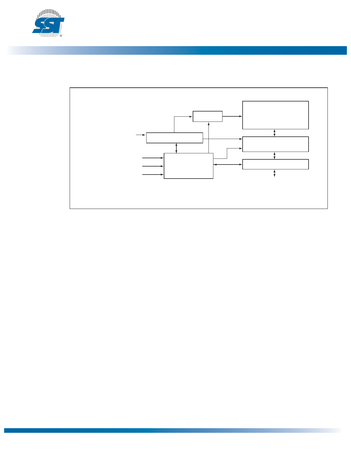
Block Diagram
Figure 1: Functional Block Diagram
Y-Decoder
I/O Buffers and Data Latches
1344 B1.0
Address Buffer Latches
X-Decoder
DQ15 - DQ0
Memory Address
OE#
CE#
WE#
SuperFlash
Memory
Control Logic
©2011 Silicon Storage Technology, Inc.
DS25031A
08/11
4
8 Mbit (x16) Multi-Purpose Flash
SST39WF800B
Data Sheet
A Microchip Technology Company
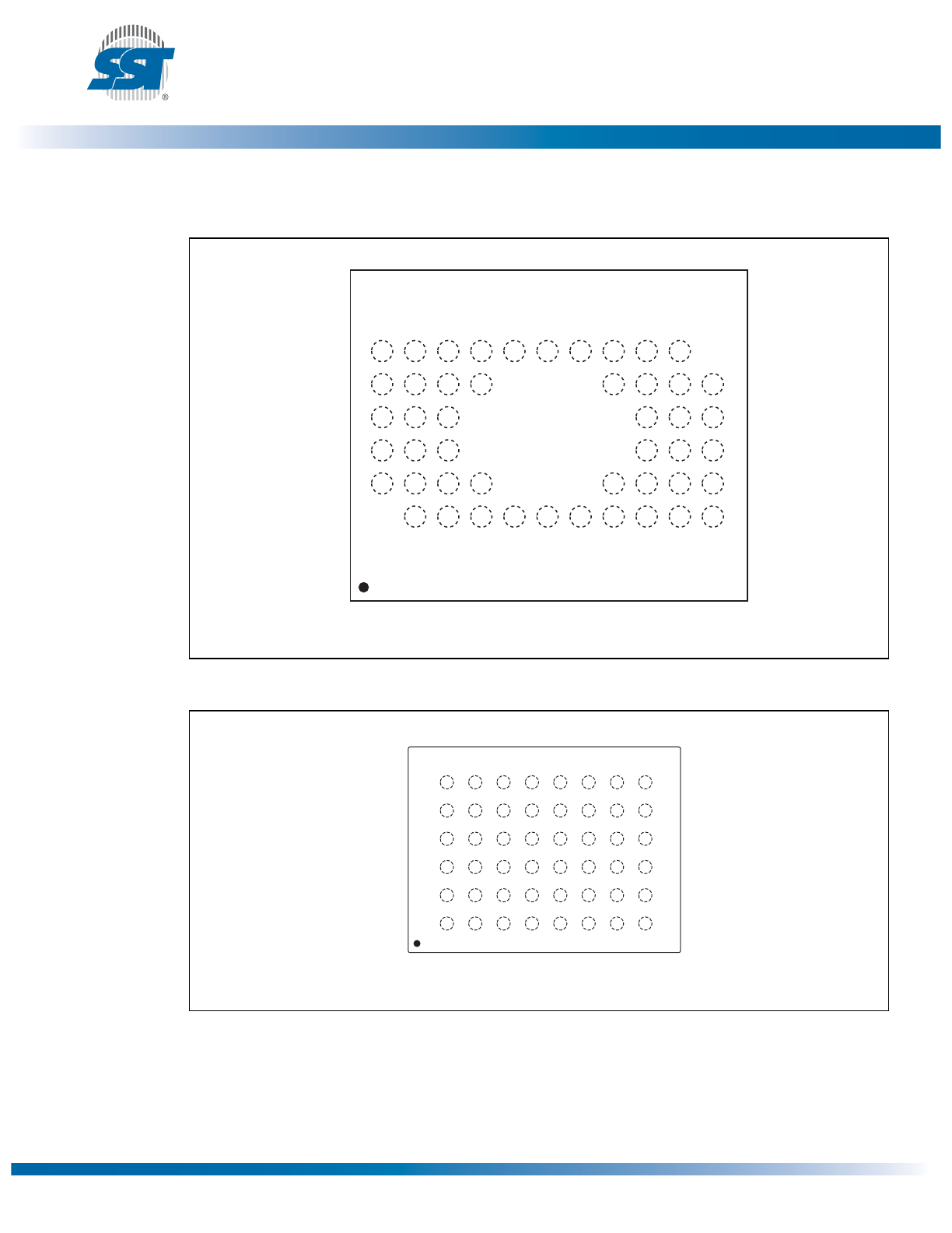
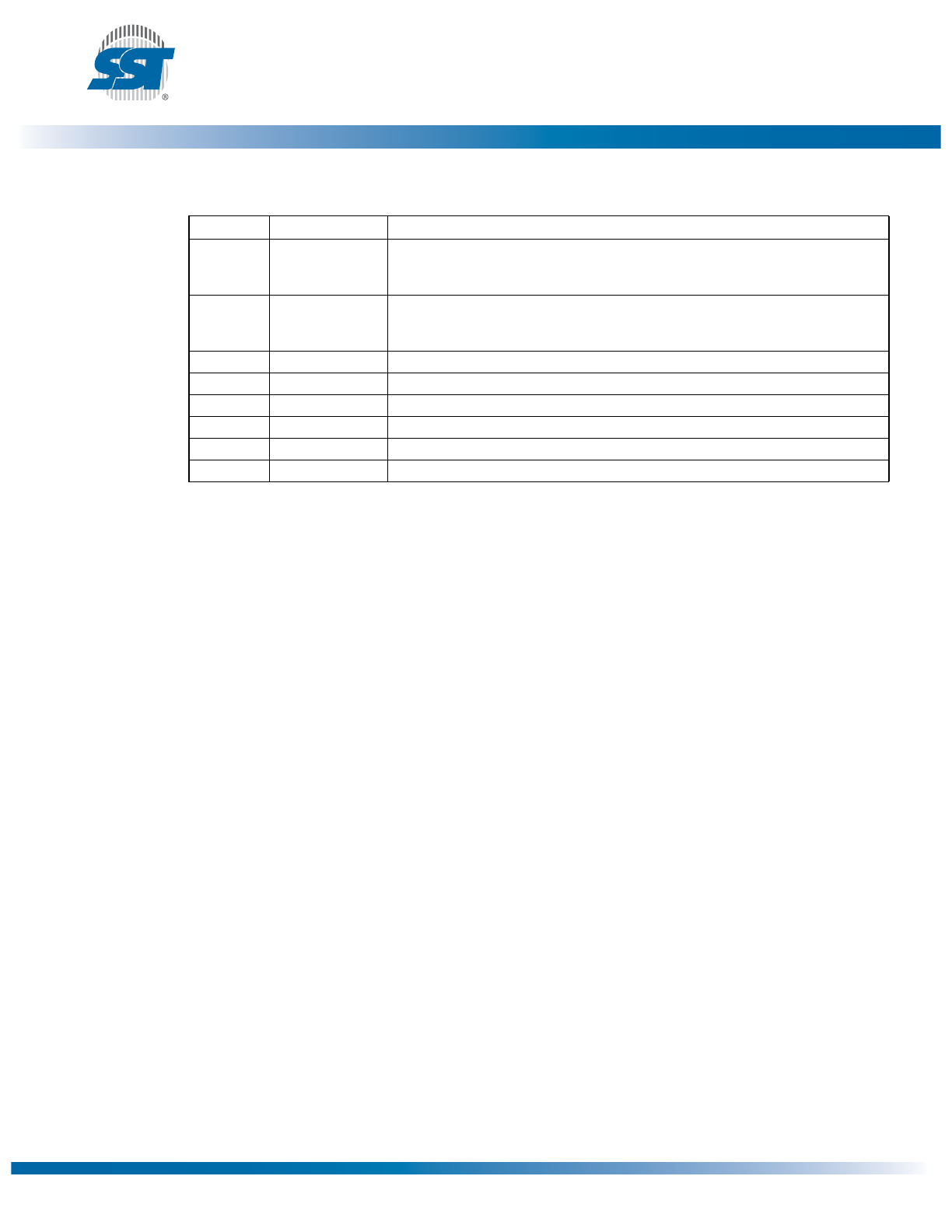
Pin Assignments
Figure 2: Pin Assignments for 48-Ball WFBGA and 48-Ball XFLGA
Figure 3: Pin Assignments for 48-ball TFBGA
A2
A1
A0
CE#
V
SS
A4
A3
A5
DQ8
OE#
DQ0
A6
A7
A18
DQ10
DQ9
DQ1
A17
NC
NC
DQ2
NC
DQ3
NC
V
DD
WE#
DQ12
NC
NC
NC
DQ13
A9
A10
A8
DQ4
DQ5
DQ14
A11
A13
A12
DQ11
DQ6
DQ15
A14
A15
A16
DQ7
V
SS
TOP VIEW (balls facing down)
A
B
C
D
E
F
G
H
J
K
L
6
5
4
3
2
1
1344 48-wfbga M2Q P02.0
SST39WF800B
1344 48-tfbga P01.0
SST39WF800B
TOP VIEW (balls facing down)
6
5
4
3
2
1
A
B
C
D
E
F
G
H
A13
A9
WE#
NC
A7
A3
A12
A8
NC
NC
A17
A4
A14
A10
NC
A18
A6
A2
A15
A11
NC
NC
A5
A1
A16
DQ7
DQ5
DQ2
DQ0
A0
NC
DQ14
DQ12
DQ10
DQ8
CE#
DQ15
DQ13
VDD
DQ11
DQ9
OE#
V
SS
DQ6
DQ4
DQ3
DQ1
V
SS
©2011 Silicon Storage Technology, Inc.
DS25031A
08/11
5
8 Mbit (x16) Multi-Purpose Flash
SST39WF800B
Data Sheet
A Microchip Technology Company
Table 1: Pin Description
Symbol
Pin Name
Functions
A
MS
1
-A
0
1. A
MS
= Most significant address
A
MS
= A
18
for SST39WF800B
Address Inputs
To provide memory addresses. During Sector-Erase A
MS
-A
11
address lines will
select the sector. During Block-Erase A
MS
-A
15
address lines will select the
block.
DQ
15
-DQ
0
Data Input/output To output data during Read cycles and receive input data during Write cycles.
Data is internally latched during a Write cycle.
The outputs are in tri-state when OE# or CE# is high.
CE#
Chip Enable
To activate the device when CE# is low.
OE#
Output Enable
To gate the data output buffers.
WE#
Write Enable
To control the Write operations.
V
DD
Power Supply
To provide power supply voltage:
1.65-1.95V for SST39WF800B
V
SS
Ground
NC
No Connection
Unconnected pins.
T1.0 25031

©2011 Silicon Storage Technology, Inc.
DS25031A
08/11
6
8 Mbit (x16) Multi-Purpose Flash
SST39WF800B
Data Sheet
A Microchip Technology Company
Device Operation
Commands, which are used to initiate the memory operation functions of the device, are written to the
device using standard microprocessor write sequences. A command is written by asserting WE# low
while keeping CE# low. The address bus is latched on the falling edge of WE# or CE#, whichever
occurs last. The data bus is latched on the rising edge of WE# or CE#, whichever occurs first.
Read
The Read operation of the SST39WF800B is controlled by CE# and OE#; both have to be low for the
system to obtain data from the outputs.
CE# is used for device selection. When CE# is high, the chip is deselected and only standby power is
consumed.
OE# is the output control and is used to gate data from the output pins. The data bus is in high imped-
ance state when either CE# or OE# is high. See Figure 5.
Word-Program Operation
The SST39WF800B is programmed on a word-by-word basis. The sector where the word exists must
be fully erased before programming.
Programming is accomplished in three steps:
1.
Load the three-byte sequence for Software Data Protection.
2.
Load word address and word data. During the Word-Program operation, the addresses
are latched on the falling edge of either CE# or WE#, whichever occurs last. The data is
latched on the rising edge of either CE# or WE#, whichever occurs first.
3.
Initiate the internal Program operation after the rising edge of the fourth WE# or CE#,
whichever occurs first. Once initiated, the Program operation will be completed within 40
µs. See Figures 6 and 7 for WE# and CE# controlled Program operation timing diagrams
and Figure 17 for flowcharts.
During the Program operation, the only valid reads are Data# Polling and Toggle Bit. During the inter-
nal Program operation, the host is free to perform additional tasks. Any commands issued during the
internal Program operation are ignored.

©2011 Silicon Storage Technology, Inc.
DS25031A
08/11
7
8 Mbit (x16) Multi-Purpose Flash
SST39WF800B
Data Sheet
A Microchip Technology Company
Sector-/Block-Erase Operation
The SST39WF800B offers both Sector-Erase and Block-Erase modes which allow the system to erase
the device on a sector-by-sector, or block-by-block, basis.
The sector architecture is based on uniform sector size of 2 KWord. Initiate the Sector-Erase operation
by executing a six-byte command sequence with Sector-Erase command (30H) and sector address
(SA) in the last bus cycle.
The Block-Erase mode is based on uniform block size of 32 KWord. Initiate the Block-Erase operation
by executing a six-byte command sequence with Block-Erase command (50H) and block address (BA)
in the last bus cycle.
The sector or block address is latched on the falling edge of the sixth WE# pulse, while the command
(30H or 50H) is latched on the rising edge of the sixth WE# pulse. The internal Erase operation begins
after the sixth WE# pulse.
The End-of-Erase operation can be determined using either Data# Polling or Toggle Bit methods. See
Figures 10 and 11 for timing waveforms. Any commands issued during the Sector- or Block-Erase
operation are ignored.
Chip-Erase Operation
The SST39WF800B provides a Chip-Erase operation, which allows the user to erase the entire mem-
ory array to the ‘1’ state. This is useful when the entire device must be quickly erased.
Initiate the Chip-Erase operation by executing a six-byte command sequence with Chip-Erase com-
mand (10H) at address 5555H in the last byte sequence.
The Erase operation begins with the rising edge of the sixth WE# or CE#, whichever occurs first. Dur-
ing the Erase operation, the only valid read is Toggle Bit or Data# Polling. See Table 4 for the command
sequence, Figure 9 for the timing diagram, and Figure 20 for the flowchart. Any commands issued dur-
ing the Chip-Erase operation are ignored.
Write Operation Status Detection
To optimize the system write cycle time, the SST39WF800B provides two software means to detect the
completion of a Program or Erase write cycle. The software detection includes two status bits—Data#
Polling (DQ
7
) and Toggle Bit (DQ
6
). The End-of-Write detection mode is enabled after the rising edge
of WE#, which initiates the internal Program or Erase operation.
The completion of the nonvolatile Write is asynchronous with the system; therefore, either a Data#
Polling or Toggle Bit read may occur simultaneously with the completion of the Write cycle. If this
occurs, the system may get an erroneous result, i.e., valid data may appear to conflict with either DQ
7
or DQ
6
. To prevent spurious rejection in the event of an erroneous result, the software routine must
include a loop to read the accessed location an additional two (2) times. If both Reads are valid, then
the device has completed the Write cycle, otherwise the rejection is valid.
©2011 Silicon Storage Technology, Inc.
DS25031A
08/11
8
8 Mbit (x16) Multi-Purpose Flash
SST39WF800B
Data Sheet
A Microchip Technology Company
Data# Polling (DQ
7
)
When the SST39WF800B is in the internal Program operation, any attempt to read DQ
7
will produce
the complement of the true data. Once the Program operation is complete, DQ
7
will produce true data.
Although DQ
7
may have valid data immediately following the completion of an internal Write operation,
the remaining data outputs may still be invalid. Valid data on the entire data bus will appear in subse-
quent successive Read cycles after an interval of 1 µs. During an internal Erase operation, any attempt
to read DQ
7
will produce a ‘0’. Once the internal Erase operation is complete, DQ
7
will produce a ‘1’.
The Data# Polling is valid after the rising edge of fourth WE# (or CE#) pulse for Program operation. For
Sector-, Block-, or Chip-Erase, the Data# Polling is valid after the rising edge of sixth WE# (or CE#)
pulse. See Figure 8 for Data# Polling timing diagram and Figure 18 for a flowchart.
Toggle Bit (DQ
6
)
During the internal Program or Erase operation, any consecutive attempts to read DQ
6
will produce
alternating ‘1’s and ‘0’s, i.e., toggling between ‘1’ and ‘0’.
When the Program or Erase operation is complete, the DQ
6
bit will stop toggling and the device is
ready for the next operation.
The Toggle Bit is valid after the rising edge of fourth WE# (or CE#) pulse for Program operation. For
Sector-, Block- or Chip-Erase, the Toggle Bit is valid after the rising edge of sixth WE# (or CE#) pulse.
See Figure 0-1 for Toggle Bit timing diagram and Figure 18 for a flowchart.
Data Protection
The SST39WF800B provides both hardware and software features to protect nonvolatile data from
inadvertent writes.
Hardware Data Protection
Noise/Glitch Protection: A WE# or CE# pulse of less than 5 ns will not initiate a write cycle.
V
DD
Power Up/Down Detection: The Write operation is inhibited when V
DD
is less than 1.0V.
Write Inhibit Mode: Forcing OE# low, CE# high, or WE# high will inhibit the Write operation. This pre-
vents inadvertent writes during power-up or power-down.
Software Data Protection (SDP)
The SST39WF800B provides the JEDEC approved Software Data Protection scheme for all data alter-
ation operations, i.e., Program and Erase. Any Program operation requires the inclusion of the three-
byte sequence. The three-byte load sequence is used to initiate the Program operation, providing opti-
mal protection from inadvertent Write operations, e.g., during the system power-up or power-down.
Any Erase operation requires the inclusion of six-byte sequence. This group of devices are shipped
with the Software Data Protection permanently enabled. See Table 4 for the specific software com-
mand codes. During SDP command sequence, invalid commands will abort the device to Read mode
within T
RC
. The contents of DQ
15
-DQ
8
can be V
IL
or V
IH
, but no other value, during any SDP command
sequence.
©2011 Silicon Storage Technology, Inc.
DS25031A
08/11
9
8 Mbit (x16) Multi-Purpose Flash
SST39WF800B
Data Sheet
A Microchip Technology Company
Common Flash Memory Interface (CFI)
The SST39WF800A contains the CFI information that describes the characteristics of the device, and
supports both the original SST CFI Query mode implementation for compatibility with existing SST
devices, as well as the general CFI Query mode.
To enter the SST CFI Query mode, the system must write the three-byte sequence, same as the Prod-
uct ID Entry command, with 98H (CFI Query command) to address 5555H in the last byte sequence.
To enter the general CFI Query mode, the system must write a one-byte sequence using the Entry
command with 98H to address 55H.
Once the device enters the CFI Query mode, the system can read CFI data at the addresses given in
Tables 5 through 7. The system must write the CFI Exit command to return to Read mode from the CFI
Query mode.
Product Identification
The Product Identification mode identifies the device as the SST39WF800B and manufacturer as SST.
This mode is accessed by software operations. Use Software Product Identification operation to iden-
tify the part (i.e., using the device ID) when using multiple manufacturers in the same socket. For
details, see Table 4 for software operation, Figure 12 for the Software ID Entry and Read timing dia-
gram, and Figure 19 for the Software ID Entry command sequence flowchart.
Product Identification Mode Exit/CFI Mode Exit
To return to the standard Read mode, exit the Software Product Identification mode. Issue the Soft-
ware ID Exit command sequence which returns the device to the Read mode.
The Software ID Exit command may also be used to reset the device to the Read mode after any inad-
vertent transient condition that causes the device to behave abnormally, e.g., not read correctly.
The Software ID Exit/CFI Exit command is ignored during an internal Program or Erase operation. See
Table 4 for software command codes, Figure 14 for timing waveform, and Figure 19 for a flowchart.
Table 2: Product Identification Table
Address
Data
Manufacturer’s ID
0000H
00BFH
Device ID
SST39WF800B
0001H
273EH
T2.0 25031
©2011 Silicon Storage Technology, Inc.
DS25031A
08/11
10
8 Mbit (x16) Multi-Purpose Flash
SST39WF800B
Data Sheet
A Microchip Technology Company
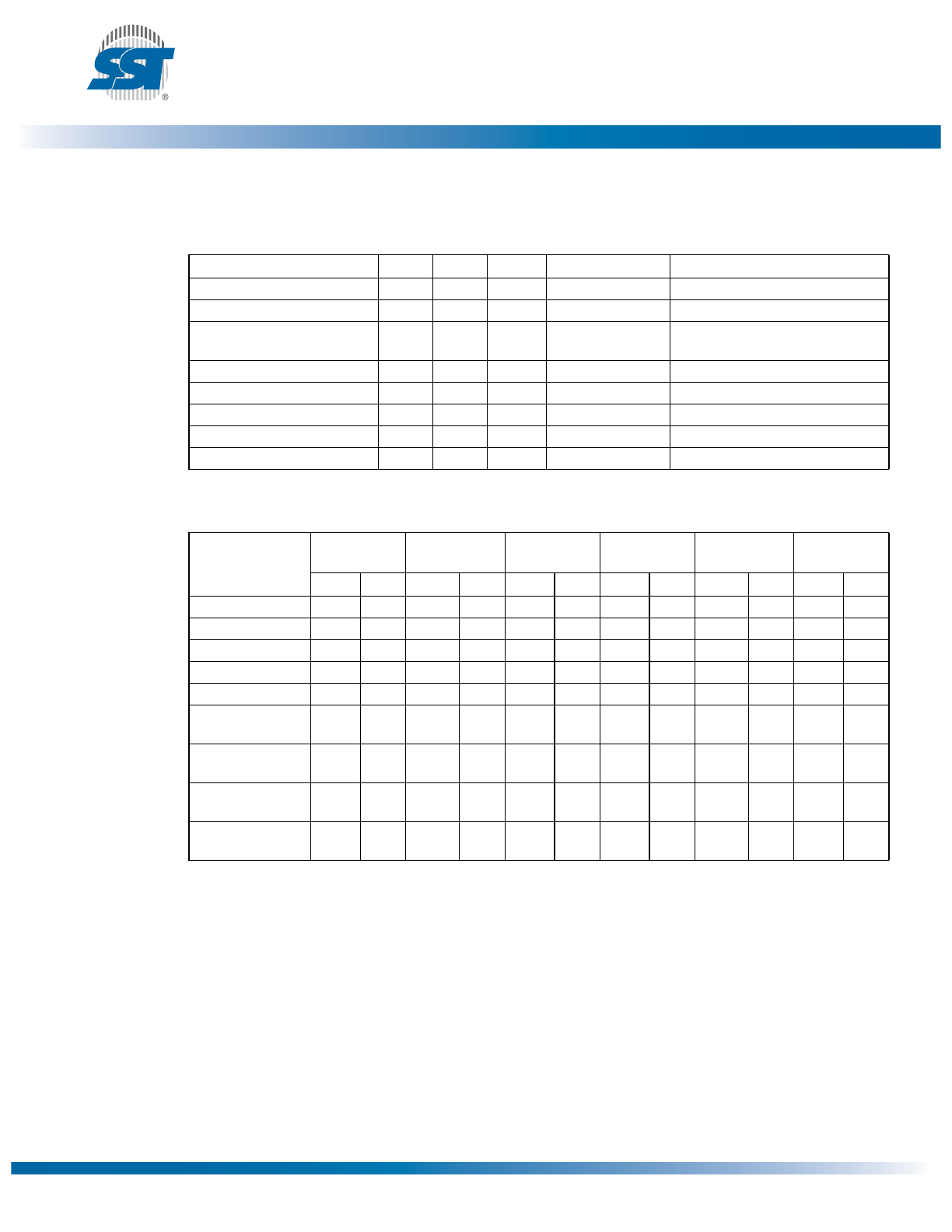
Operations
Table 3: Operation Modes Selection
Mode
CE#
OE#
WE#
DQ
Address
Read
V
IL
V
IL
V
IH
D
OUT
A
IN
Program
V
IL
V
IH
V
IL
D
IN
A
IN
Erase
V
IL
V
IH
V
IL
X
1
1. X can be V
IL
or V
IH
, but no other value.
Sector or Block address,
XXH for Chip-Erase
Standby
V
IH
X
X
High Z
X
Write Inhibit
X
V
IL
X
High Z/ D
OUT
X
X
X
V
IH
High Z/ D
OUT
X
Product Identification
Software Mode
V
IL
V
IL
V
IH
See Table 4
T3.0 25031
Table 4: Software Command Sequence
Command
Sequence
1st Bus
Write Cycle
2nd Bus
Write Cycle
3rd Bus
Write Cycle
4th Bus
Write Cycle
5th Bus
Write Cycle
6th Bus
Write Cycle
Addr
1
1. Address format A
14
-A
0
(Hex), Addresses A
MS-
A
15
can be V
IL
or V
IH
, but no other value, for the Command sequence.
A
MS
= Most significant address
A
MS
= A
18
for SST39WF800B
Data
2
2. DQ
15
-DQ
8
can be V
IL
or V
IH
, but no other value, for the Command sequence
Addr
1
Data
2
Addr
1
Data
2
Addr
1
Data
2
Addr
1
Data
2
Addr
1
Data
2
Word-Program
5555H
AAH
2AAAH
55H
5555H
A0H
WA
3
3. WA = Program word address
Data
Sector-Erase
5555H
AAH
2AAAH
55H
5555H
80H
5555H
AAH
2AAAH
55H
SA
X
4
4. SA
X
for Sector-Erase; uses A
MS
-A
11
address lines
BA
X
for Block-Erase; uses A
MS
-A
15
address lines
30H
Block-Erase
5555H
AAH
2AAAH
55H
5555H
80H
5555H
AAH
2AAAH
55H
BA
X
4
50H
Chip-Erase
5555H
AAH
2AAAH
55H
5555H
80H
5555H
AAH
2AAAH
55H
5555H
10H
Software ID Entry
5,6
5. The device does not remain in Software Product ID mode if powered down.
6. With A
MS
-A
1
= 0;
SST Manufacturer’s ID = 00BFH, is read with A
0
= 0,
SST39WF800B Device ID = 273EH, is read with A
0
= 1.
5555H
AAH
2AAAH
55H
5555H
90H
SST CFI Query
Entry
5
5555H
AAH
2AAAH
55H
5555H
98H
General CFI Query
Mode
55H
98H
Software ID Exit
7
/
CFI Exit
7. Both Software ID Exit operations are equivalent
XXH
F0H
Software ID Exit
7
/
CFI Exit
5555H
AAH
2AAAH
55H
5555H
F0H
T4.0 25031