

A Microchip Technology Company
©2011 Silicon Storage Technology, Inc.
DS25028A
08/11
Not Recommended for New Designs
www.microchip.com
16 Mbit / 32 Mbit / (x16) Multi-Purpose Flash Plus
SST39VF1601 / SST39VF3201
SST39VF1602 / SST39VF3202
Features
• Organized as 1M x16: SST39VF1601/1602
2M x16: SST39VF3201/3202
• Single Voltage Read and Write Operations
– 2.7-3.6V
• Superior Reliability
– Endurance: 100,000 Cycles (Typical)
– Greater than 100 years Data Retention
• Low Power Consumption (typical values at 5 MHz)
– Active Current: 9 mA (typical)
– Standby Current: 3 µA (typical)
– Auto Low Power Mode: 3 µA (typical)
• Hardware Block-Protection/WP# Input Pin
– Top Block-Protection (top 32 KWord)
for SST39VF1602/3202
– Bottom Block-Protection (bottom 32 KWord)
for SST39VF1601/3201
• Sector-Erase Capability
– Uniform 2 KWord sectors
• Block-Erase Capability
– Uniform 32 KWord blocks
• Chip-Erase Capability
• Erase-Suspend/Erase-Resume Capabilities
• Hardware Reset Pin (RST#)
• Security-ID Feature
– SST: 128 bits; User: 128 bits
• Fast Read Access Time:
– 70 ns
• Latched Address and Data
• Fast Erase and Word-Program:
– Sector-Erase Time: 18 ms (typical)
– Block-Erase Time: 18 ms (typical)
– Chip-Erase Time: 40 ms (typical)
– Word-Program Time: 7 µs (typical)
• Automatic Write Timing
– Internal V
PP
Generation
• End-of-Write Detection
– Toggle Bits
– Data# Polling
• CMOS I/O Compatibility
• JEDEC Standard
– Flash EEPROM Pinouts and command sets
• Packages Available
– 48-lead TSOP (12mm x 20mm)
– 48-ball TFBGA (6mm x 8mm)
• All devices are RoHS compliant
The SST39VF1601/1602 and SST39VF3201/3202 devices are 1M x16 and 2M
x16, respectively, CMOS Multi-Purpose Flash Plus (MPF+) manufactured with
SST's proprietary, high performance CMOS SuperFlash technology. The split-
gate cell design and thick-oxide tunneling injector attain better reliability and man-
ufacturability compared with alternate approaches. The SST39VF1601/1602/
3201/3202 write (Program or Erase) with a 2.7-3.6V power supply. These devices
conforms to JEDEC standard pinouts for x16 memories.
Not recommended for new designs. Please use SST39VF1601C
and SST39VF3201B.

©2011 Silicon Storage Technology, Inc.
DS25028A
08/11
2
16 Mbit / 32 Mbit Multi-Purpose Flash Plus
SST39VF1601 / SST39VF3201
SST39VF1602 / SST39VF3202
Not Recommended for New Designs
A Microchip Technology Company
Product Description
The SST39VF160x and SST39VF320x devices are 1M x16 and 2M x16, respectively, CMOS Multi-
Purpose Flash Plus (MPF+) manufactured with SST’s proprietary, high performance CMOS Super-
Flash technology. The split-gate cell design and thick-oxide tunneling injector attain better reliability
and manufacturability compared with alternate approaches. The SST39VF160x/320x write (Program
or Erase) with a 2.7-3.6V power supply. These devices conform to JEDEC standard pinouts for x16
memories.
Featuring high performance Word-Program, the SST39VF160x/320x devices provide a typical Word-
Program time of 7 µsec. These devices use Toggle Bit or Data# Polling to indicate the completion of
Program operation. To protect against inadvertent write, they have on-chip hardware and Software
Data Protection schemes. Designed, manufactured, and tested for a wide spectrum of applications,
these devices are offered with a guaranteed typical endurance of 100,000 cycles. Data retention is
rated at greater than 100 years.
The SST39VF160x/320x devices are suited for applications that require convenient and economical
updating of program, configuration, or data memory. For all system applications, they significantly
improve performance and reliability, while lowering power consumption. They inherently use less
energy during Erase and Program than alternative flash technologies. The total energy consumed is a
function of the applied voltage, current, and time of application. Since for any given voltage range, the
SuperFlash technology uses less current to program and has a shorter erase time, the total energy
consumed during any Erase or Program operation is less than alternative flash technologies. These
devices also improve flexibility while lowering the cost for program, data, and configuration storage
applications.
The SuperFlash technology provides fixed Erase and Program times, independent of the number of
Erase/Program cycles that have occurred. Therefore the system software or hardware does not have
to be modified or de-rated as is necessary with alternative flash technologies, whose Erase and Pro-
gram times increase with accumulated Erase/Program cycles.
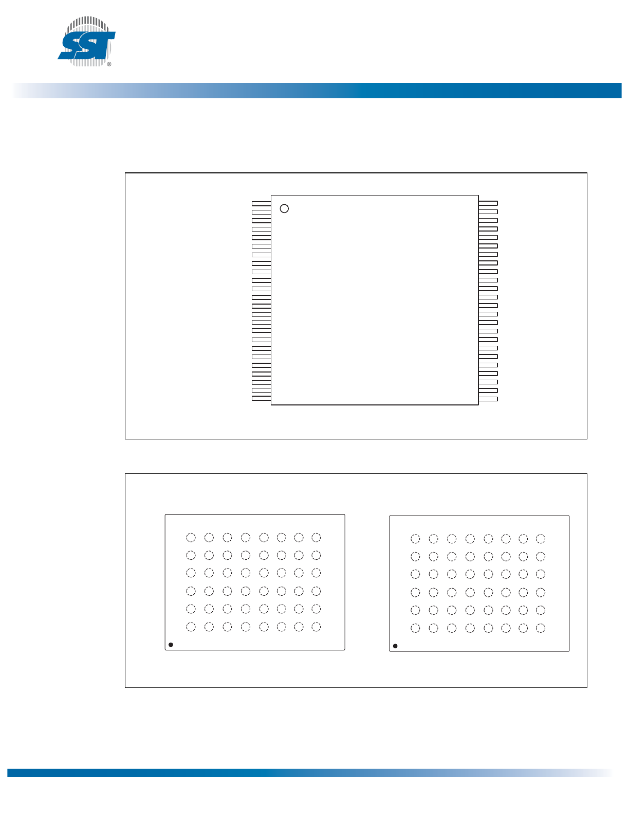
To meet high density, surface mount requirements, the SST39VF160x/320x are offered in 48-lead
TSOP and 48-ball TFBGA packages. See Figures 2 and 3 for pin assignments.
©2011 Silicon Storage Technology, Inc.
DS25028A
08/11
3
16 Mbit / 32 Mbit Multi-Purpose Flash Plus
SST39VF1601 / SST39VF3201
SST39VF1602 / SST39VF3202
Not Recommended for New Designs
A Microchip Technology Company
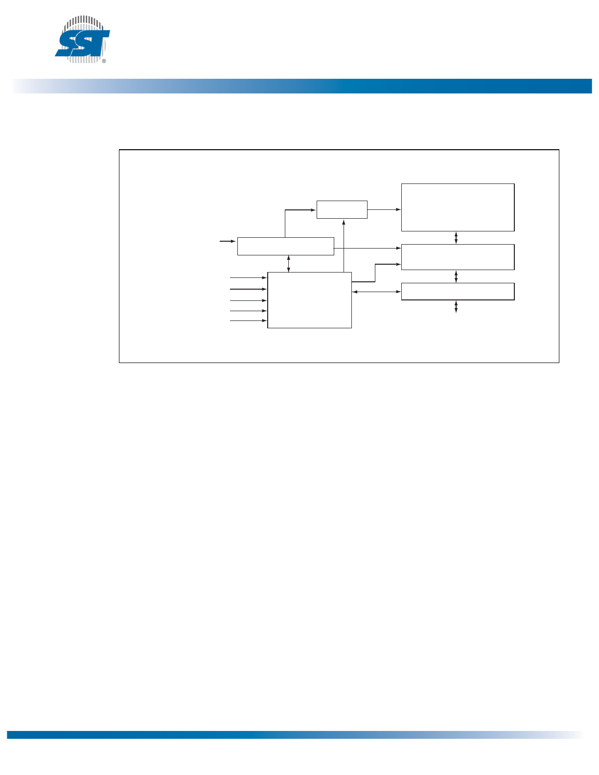
Block Diagram
Figure 1: Functional Block Diagram
Y-Decoder
I/O Buffers and Data Latches
1223 B1.0
Address Buffer Latches
X-Decoder
DQ
15
- DQ
0
Memory Address
OE#
CE#
WE#
SuperFlash
Memory
Control Logic
WP#
RESET#
©2011 Silicon Storage Technology, Inc.
DS25028A
08/11
4
16 Mbit / 32 Mbit Multi-Purpose Flash Plus
SST39VF1601 / SST39VF3201
SST39VF1602 / SST39VF3202
Not Recommended for New Designs
A Microchip Technology Company
Pin Assignment
Figure 2: Pin Assignments for 48-lead TSOP
Figure 3: pin assignments for 48-ball TFBGA
A15
A14
A13
A12
A11
A10
A9
A8
A19
A20
WE#
RST#
NC
WP#
NC
A18
A17
A7
A6
A5
A4
A3
A2
A1
1
2
3
4
5
6
7
8
9
10
11
12
13
14
15
16
17
18
19
20
21
22
23
24
A16
NC
VSS
DQ15
DQ7
DQ14
DQ6
DQ13
DQ5
DQ12
DQ4
VDD
DQ11
DQ3
DQ10
DQ2
DQ9
DQ1
DQ8
DQ0
OE#
VSS
CE#
A0
48
47
46
45
44
43
42
41
40
39
38
37
36
35
34
33
32
31
30
29
28
27
26
25
1223 48-tsop P01.4
Standard Pinout
Top View
Die Up
SST39VF160x/320x
A15
A14
A13
A12
A11
A10
A9
A8
A19
NC
WE#
RST#
NC
WP#
NC
A18
A17
A7
A6
A5
A4
A3
A2
A1
SST39VF1601/1602
SST39VF3201/3202
A13
A9
WE#
NC
A7
A3
A12
A8
RST#
WP#
A17
A4
A14
A10
NC
A18
A6
A2
A15
A11
A19
A20
A5
A1
A16
DQ7
DQ5
DQ2
DQ0
A0
NC
DQ14
DQ12
DQ10
DQ8
CE#
DQ15
DQ13
VDD
DQ11
DQ9
OE#
VSS
DQ6
DQ4
DQ3
DQ1
VSS
1223 48-tfbga B3K P02a.2
SST39VF3201/3202
TOP VIEW (balls facing down)
6
5
4
3
2
1
A
B
C
D
E
F
G
H
A13
A9
WE#
NC
A7
A3
A12
A8
RST#
WP#
A17
A4
A14
A10
NC
A18
A6
A2
A15
A11
A19
NC
A5
A1
A16
DQ7
DQ5
DQ2
DQ0
A0
NC
DQ14
DQ12
DQ10
DQ8
CE#
DQ15
DQ13
VDD
DQ11
DQ9
OE#
VSS
DQ6
DQ4
DQ3
DQ1
VSS
1223 48-tfbga B3K P02.0
SST39VF1601/1602
TOP VIEW (balls facing down)
6
5
4
3
2
1
A
B
C
D
E
F
G
H
©2011 Silicon Storage Technology, Inc.
DS25028A
08/11
5
16 Mbit / 32 Mbit Multi-Purpose Flash Plus
SST39VF1601 / SST39VF3201
SST39VF1602 / SST39VF3202
Not Recommended for New Designs
A Microchip Technology Company
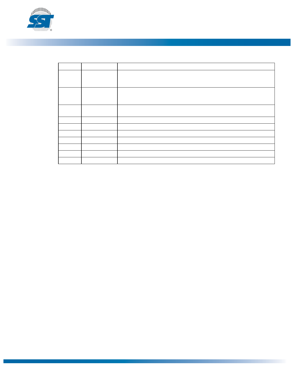
Table 1: Pin Description
Symbol
Pin Name
Functions
A
MS
1
-A
0
Address Inputs
To provide memory addresses.
During Sector-Erase A
MS
-A
11
address lines will select the sector.
During Block-Erase A
MS
-A
15
address lines will select the block.
DQ
15
-DQ
0
Data Input/output To output data during Read cycles and receive input data during Write cycles.
Data is internally latched during a Write cycle.
The outputs are in tri-state when OE# or CE# is high.
WP#
Write Protect
To protect the top/bottom boot block from Erase/Program operation when
grounded.
RST#
Reset
To reset and return the device to Read mode.
CE#
Chip Enable
To activate the device when CE# is low.
OE#
Output Enable
To gate the data output buffers.
WE#
Write Enable
To control the Write operations.
V
DD
Power Supply
To provide power supply voltage: 2.7-3.6V
V
SS
Ground
NC
No Connection
Unconnected pins.
T1.2 25028
1. A
MS
= Most significant address
A
MS
= A
19
for SST39VF1601/1602, and A
20
for SST39VF3201/3202

©2011 Silicon Storage Technology, Inc.
DS25028A
08/11
6
16 Mbit / 32 Mbit Multi-Purpose Flash Plus
SST39VF1601 / SST39VF3201
SST39VF1602 / SST39VF3202
Not Recommended for New Designs
A Microchip Technology Company
Device Operation
Commands are used to initiate the memory operation functions of the device. Commands are written
to the device using standard microprocessor write sequences. A command is written by asserting WE#
low while keeping CE# low. The address bus is latched on the falling edge of WE# or CE#, whichever
occurs last. The data bus is latched on the rising edge of WE# or CE#, whichever occurs first.
The SST39VF160x/320x also have the Auto Low Power mode which puts the device in a near
standby mode after data has been accessed with a valid Read operation. This reduces the I
DD
active
read current from typically 9 mA to typically 3 µA. The Auto Low Power mode reduces the typical I
DD
active read current to the range of 2 mA/MHz of Read cycle time. The device exits the Auto Low Power
mode with any address transition or control signal transition used to initiate another Read cycle, with
no access time penalty. Note that the device does not enter Auto-Low Power mode after power-up with
CE# held steadily low, until the first address transition or CE# is driven high.
Read
The Read operation of the SST39VF160x/320x is controlled by CE# and OE#, both have to be low for
the system to obtain data from the outputs. CE# is used for device selection. When CE# is high, the
chip is deselected and only standby power is consumed. OE# is the output control and is used to gate
data from the output pins. The data bus is in high impedance state when either CE# or OE# is high.
Refer to the Read cycle timing diagram for further details (Figure 4).
Word-Program Operation
The SST39VF160x/320x are programmed on a word-by-word basis. Before programming, the sector
where the word exists must be fully erased. The Program operation is accomplished in three steps.
The first step is the three-byte load sequence for Software Data Protection. The second step is to load
word address and word data. During the Word-Program operation, the addresses are latched on the
falling edge of either CE# or WE#, whichever occurs last. The data is latched on the rising edge of
either CE# or WE#, whichever occurs first. The third step is the internal Program operation which is ini-
tiated after the rising edge of the fourth WE# or CE#, whichever occurs first. The Program operation,
once initiated, will be completed within 10 µs. See Figures 5 and 6 for WE# and CE# controlled Pro-
gram operation timing diagrams and Figure 20 for flowcharts. During the Program operation, the only
valid reads are Data# Polling and Toggle Bit. During the internal Program operation, the host is free to
perform additional tasks. Any commands issued during the internal Program operation are ignored.
During the command sequence, WP# should be statically held high or low.
Sector/Block-Erase Operation
The Sector- (or Block-) Erase operation allows the system to erase the device on a sector-by-sector (or
block-by-block) basis. The SST39VF160x/320x offer both Sector-Erase and Block-Erase mode. The
sector architecture is based on uniform sector size of 2 KWord. The Block-Erase mode is based on
uniform block size of 32 KWord. The Sector-Erase operation is initiated by executing a six-byte com-
mand sequence with Sector-Erase command (30H) and sector address (SA) in the last bus cycle. The
Block-Erase operation is initiated by executing a six-byte command sequence with Block-Erase com-
mand (50H) and block address (BA) in the last bus cycle. The sector or block address is latched on the
falling edge of the sixth WE# pulse, while the command (30H or 50H) is latched on the rising edge of
the sixth WE# pulse. The internal Erase operation begins after the sixth WE# pulse. The End-of-Erase
operation can be determined using either Data# Polling or Toggle Bit methods. See Figures 10 and 11

©2011 Silicon Storage Technology, Inc.
DS25028A
08/11
7
16 Mbit / 32 Mbit Multi-Purpose Flash Plus
SST39VF1601 / SST39VF3201
SST39VF1602 / SST39VF3202
Not Recommended for New Designs
A Microchip Technology Company
for timing waveforms and Figure 24 for the flowchart. Any commands issued during the Sector- or
Block-Erase operation are ignored. When WP# is low, any attempt to Sector- (Block-) Erase the pro-
tected block will be ignored. During the command sequence, WP# should be statically held high or low.
Erase-Suspend/Erase-Resume Commands
The Erase-Suspend operation temporarily suspends a Sector- or Block-Erase operation thus allowing
data to be read from any memory location, or program data into any sector/block that is not suspended
for an Erase operation. The operation is executed by issuing one byte command sequence with Erase-
Suspend command (B0H). The device automatically enters read mode typically within 20 µs after the
Erase-Suspend command had been issued. Valid data can be read from any sector or block that is not
suspended from an Erase operation. Reading at address location within erase-suspended sectors/
blocks will output DQ
2
toggling and DQ
6
at “1”. While in Erase-Suspend mode, a Word-Program oper-
ation is allowed except for the sector or block selected for Erase-Suspend.
To resume Sector-Erase or Block-Erase operation which has been suspended the system must issue
Erase Resume command. The operation is executed by issuing one byte command sequence with
Erase Resume command (30H) at any address in the last Byte sequence.
Chip-Erase Operation
The SST39VF160x/320x provide a Chip-Erase operation, which allows the user to erase the entire
memory array to the “1” state. This is useful when the entire device must be quickly erased.
The Chip-Erase operation is initiated by executing a six-byte command sequence with Chip-Erase
command (10H) at address 5555H in the last byte sequence. The Erase operation begins with the ris-
ing edge of the sixth WE# or CE#, whichever occurs first. During the Erase operation, the only valid
read is Toggle Bit or Data# Polling. See Table 6 for the command sequence, Figure 10 for timing dia-
gram, and Figure 24 for the flowchart. Any commands issued during the Chip-Erase operation are
ignored. When WP# is low, any attempt to Chip-Erase will be ignored. During the command sequence,
WP# should be statically held high or low.
Write Operation Status Detection
The SST39VF160x/320x provide two software means to detect the completion of a Write (Program or
Erase) cycle, in order to optimize the system write cycle time. The software detection includes two sta-
tus bits: Data# Polling (DQ
7
) and Toggle Bit (DQ
6
). The End-of-Write detection mode is enabled after
the rising edge of WE#, which initiates the internal Program or Erase operation.
The actual completion of the nonvolatile write is asynchronous with the system; therefore, either a
Data# Polling or Toggle Bit read may be simultaneous with the completion of the write cycle. If this
occurs, the system may possibly get an erroneous result, i.e., valid data may appear to conflict with
either DQ
7
or DQ
6
. In order to prevent spurious rejection, if an erroneous result occurs, the software
routine should include a loop to read the accessed location an additional two (2) times. If both reads
are valid, then the device has completed the Write cycle, otherwise the rejection is valid.
©2011 Silicon Storage Technology, Inc.
DS25028A
08/11
8
16 Mbit / 32 Mbit Multi-Purpose Flash Plus
SST39VF1601 / SST39VF3201
SST39VF1602 / SST39VF3202
Not Recommended for New Designs
A Microchip Technology Company
Data# Polling (DQ
7
)
When the SST39VF160x/320x are in the internal Program operation, any attempt to read DQ
7
will pro-
duce the complement of the true data. Once the Program operation is completed, DQ
7
will produce
true data. Note that even though DQ
7
may have valid data immediately following the completion of an internal
Write operation, the remaining data outputs may still be invalid: valid data on the entire data bus will appear in
subsequent successive Read cycles after an interval of 1 µs. During internal Erase operation, any attempt
to read DQ
7
will produce a ‘0’. Once the internal Erase operation is completed, DQ
7
will produce a ‘1’.
The Data# Polling is valid after the rising edge of fourth WE# (or CE#) pulse for Program operation. For
Sector-, Block- or Chip-Erase, the Data# Polling is valid after the rising edge of sixth WE# (or CE#)
pulse. See Figure 7 for Data# Polling timing diagram and Figure 21 for a flowchart.
Toggle Bits (DQ6 and DQ2)
During the internal Program or Erase operation, any consecutive attempts to read DQ
6
will produce
alternating “1”s and “0”s, i.e., toggling between 1 and 0. When the internal Program or Erase operation
is completed, the DQ
6
bit will stop toggling. The device is then ready for the next operation. For Sector-
, Block-, or Chip-Erase, the toggle bit (DQ
6
) is valid after the rising edge of sixth WE# (or CE#) pulse.
DQ
6
will be set to “1” if a Read operation is attempted on an Erase-Suspended Sector/Block. If Pro-
gram operation is initiated in a sector/block not selected in Erase-Suspend mode, DQ
6
will toggle.
An additional Toggle Bit is available on DQ
2
, which can be used in conjunction with DQ
6
to check
whether a particular sector is being actively erased or erase-suspended. Table 2 shows detailed status
bits information. The Toggle Bit (DQ
2
) is valid after the rising edge of the last WE# (or CE#) pulse of
Write operation. See Figure 8 for Toggle Bit timing diagram and Figure 21 for a flowchart.
Note: DQ
7
and DQ
2
require a valid address when reading status information.
Data Protection
The SST39VF160x/320x provide both hardware and software features to protect nonvolatile data from
inadvertent writes.
Hardware Data Protection
Noise/Glitch Protection: A WE# or CE# pulse of less than 5 ns will not initiate a write cycle.
V
DD
Power Up/Down Detection: The Write operation is inhibited when V
DD
is less than 1.5V.
Write Inhibit Mode: Forcing OE# low, CE# high, or WE# high will inhibit the Write operation. This pre-
vents inadvertent writes during power-up or power-down.
Table 2: Write Operation Status
Status
DQ
7
DQ
6
DQ
2
Normal Operation
Standard Program
DQ
7
#
Toggle
No Toggle
Standard Erase
0
Toggle
Toggle
Erase-Suspend Mode
Read from Erase-Suspended Sector/Block
1
1
Toggle
Read from Non- Erase-Suspended Sector/Block
Data
Data
Data
Program
DQ
7
#
Toggle
N/A
T2.0 25028
©2011 Silicon Storage Technology, Inc.
DS25028A
08/11
9
16 Mbit / 32 Mbit Multi-Purpose Flash Plus
SST39VF1601 / SST39VF3201
SST39VF1602 / SST39VF3202
Not Recommended for New Designs
A Microchip Technology Company
Hardware Block Protection
The SST39VF1602/3202 support top hardware block protection, which protects the top 32 KWord
block of the device. The SST39VF1601/3201 support bottom hardware block protection, which pro-
tects the bottom 32 KWord block of the device. The Boot Block address ranges are described in Table
3. Program and Erase operations are prevented on the 32 KWord when WP# is low. If WP# is left float-
ing, it is internally held high via a pull-up resistor, and the Boot Block is unprotected, enabling Program
and Erase operations on that block.
Hardware Reset (RST#)
The RST# pin provides a hardware method of resetting the device to read array data. When the RST#
pin is held low for at least T
RP,
any in-progress operation will terminate and return to Read mode. When
no internal Program/Erase operation is in progress, a minimum period of T
RHR
is required after RST#
is driven high before a valid Read can take place (see Figure 16).
The Erase or Program operation that has been interrupted needs to be reinitiated after the device
resumes normal operation mode to ensure data integrity.
Software Data Protection (SDP)
The SST39VF160x/320x provide the JEDEC approved Software Data Protection scheme for all data
alteration operations, i.e., Program and Erase. Any Program operation requires the inclusion of the
three-byte sequence. The three-byte load sequence is used to initiate the Program operation, provid-
ing optimal protection from inadvertent Write operations, e.g., during the system power-up or power-
down. Any Erase operation requires the inclusion of six-byte sequence. These devices are shipped
with the Software Data Protection permanently enabled. See Table 6 for the specific software com-
mand codes. During SDP command sequence, invalid commands will abort the device to read mode
within T
RC.
The contents of DQ
15
-DQ
8
can be V
IL
or V
IH
, but no other value, during any SDP command
sequence.
Common Flash Memory Interface (CFI)
The SST39VF160x/320x also contain the CFI information to describe the characteristics of the device.
In order to enter the CFI Query mode, the system must write three-byte sequence, same as product ID
entry command with 98H (CFI Query command) to address 5555H in the last byte sequence. Once the
device enters the CFI Query mode, the system can read CFI data at the addresses given in Tables 7
through 10. The system must write the CFI Exit command to return to Read mode from the CFI Query
mode.
Table 3: Boot Block Address Ranges
Product
Address Range
Bottom Boot Block
SST39VF1601/3201
000000H-007FFFH
Top Boot Block
SST39VF1602
0F8000H-0FFFFFH
SST39VF3202
1F8000H-1FFFFFH
T3.0 25028
©2011 Silicon Storage Technology, Inc.
DS25028A
08/11
10
16 Mbit / 32 Mbit Multi-Purpose Flash Plus
SST39VF1601 / SST39VF3201
SST39VF1602 / SST39VF3202
Not Recommended for New Designs
A Microchip Technology Company
Product Identification
The Product Identification mode identifies the devices as the SST39VF1601, SST39VF1602,
SST39VF3201, or SST39VF3202, and manufacturer as SST. This mode may be accessed software
operations. Users may use the Software Product Identification operation to identify the part (i.e., using
the device ID) when using multiple manufacturers in the same socket. For details, see Table 6 for soft-
ware operation, Figure 12 for the Software ID Entry and Read timing diagram and Figure 22 for the
Software ID Entry command sequence flowchart.
Product Identification Mode Exit/CFI Mode Exit
In order to return to the standard Read mode, the Software Product Identification mode must be exited.
Exit is accomplished by issuing the Software ID Exit command sequence, which returns the device to
the Read mode. This command may also be used to reset the device to the Read mode after any inad-
vertent transient condition that apparently causes the device to behave abnormally, e.g., not read cor-
rectly. Please note that the Software ID Exit/CFI Exit command is ignored during an internal Program
or Erase operation. See Table 6 for software command codes, Figure 14 for timing waveform, and Fig-
ures 22 and 23 for flowcharts.
Security ID
The SST39VF160x/320x devices offer a 256-bit Security ID space. The Secure ID space is divided into
two 128-bit segments - one factory programmed segment and one user programmed segment. The
first segment is programmed and locked at SST with a random 128-bit number. The user segment is
left un-programmed for the customer to program as desired.
To program the user segment of the Security ID, the user must use the Security ID Word-Program
command. To detect end-of-write for the SEC ID, read the toggle bits. Do not use Data# Polling. Once
this is complete, the Sec ID should be locked using the User Sec ID Program Lock-Out. This disables
any future corruption of this space. Note that regardless of whether or not the Sec ID is locked, neither
Sec ID segment can be erased.
The Secure ID space can be queried by executing a three-byte command sequence with Enter Sec ID
command (88H) at address 5555H in the last byte sequence. To exit this mode, the Exit Sec ID com-
mand should be executed. Refer to Table 6 for more details.
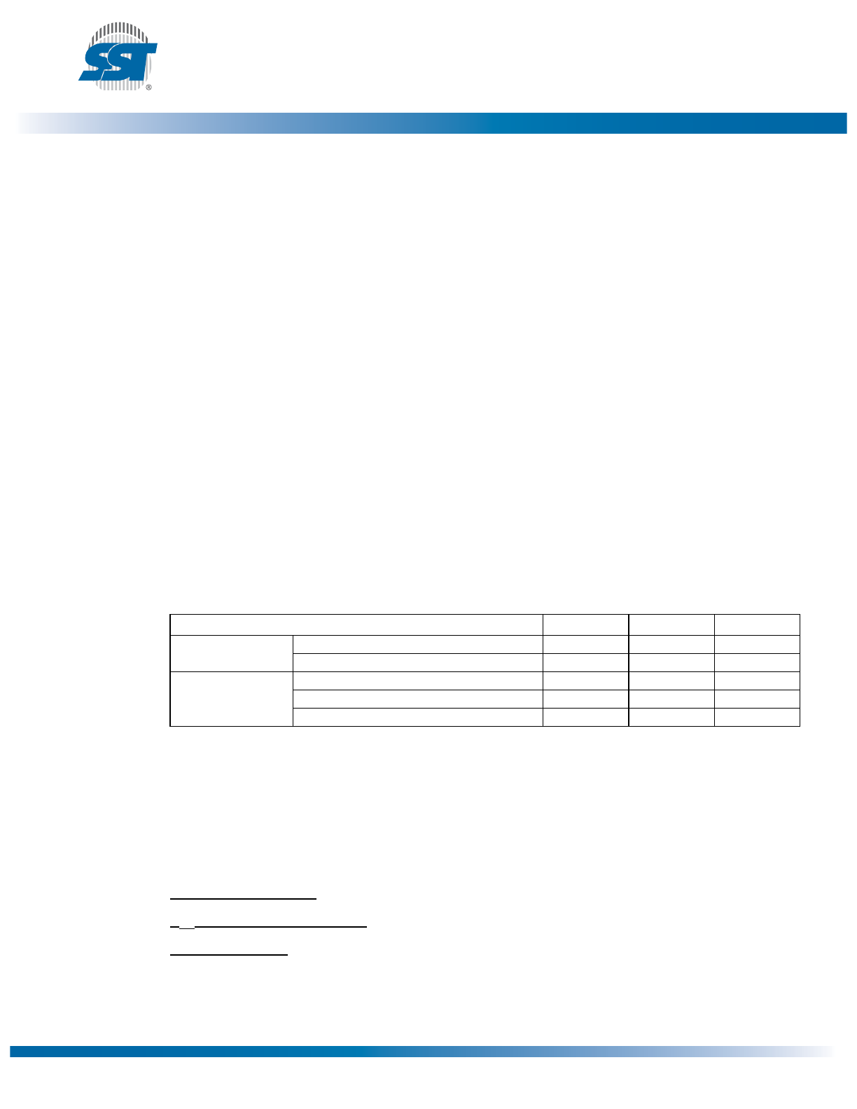
Table 4: Product Identification
Address
Data
Manufacturer’s ID
0000H
BFH
Device ID
SST39VF1601
0001H
234BH
SST39VF1602
0001H
234AH
SST39VF3201
0001H
235BH
SST39VF3202
0001H
235AH
T4.2 25028