

A Microchip Technology Company
©2011 Silicon Storage Technology, Inc.
DS-25017A
04/11
Data Sheet
www.microchip.com
Features
• Single Voltage Read and Write Operations
– 2.7-3.6V
• Serial Interface Architecture
– Nibble-wide multiplexed I/O’s with SPI-like serial com-
mand structure
- Mode 0 and Mode 3
– Single-bit, SPI backwards compatible
- Read, High-Speed Read, and JEDEC ID Read
• High Speed Clock Frequency
– 80 MHz
- 320 Mbit/s sustained data rate
• Burst Modes
– Continuous linear burst
– 8/16/32/64 Byte linear burst with wrap-around
• Index Jump
– Jump to address index within 256 Byte Page
– Jump to address index within 64 KByte Block
– Jump to address index in another 64 KByte Block
• Superior Reliability
– Endurance: 100,000 cycles
– Greater than 100 years data retention
• Low Power Consumption:
– Active Read current: 12 mA (typical @ 80 MHz)
– Standby current: 8 µA (typical)
• Fast Erase and Byte-Program:
– Chip-Erase time: 35 ms (typical)
– Sector-/Block-Erase time: 18 ms (typical)
• Page-Program
– 256 Bytes per page
– Fast Page Program time in 1 ms (typical)
• End-of-Write Detection
– Software polling the BUSY bit in status register
• Flexible Erase Capability
– Uniform 4 KByte sectors
– Four 8 KByte top parameter overlay blocks
– Four 8 KByte bottom parameter overlay blocks
– Two 32 KByte overlay blocks (one each top and bottom)
– Uniform 64 KByte overlay blocks
- SST26VF016 – 30 blocks
- SST26VF032 – 62 blocks
• Write-Suspend
– Suspend program or Erase operation to access another
block/sector
• Software Reset (RST) mode
• Software Write Protection
– Block-Locking
- 64 KByte blocks, two 32 KByte blocks, and eight 8
KByte parameter blocks
• Security ID
– One-Time Programmable (OTP) 256 bit, Secure ID
- 64 bit Unique, factory pre-programmed identifier
- 192 bit user-programmable
• Temperature Range
– Industrial: -40°C to +85°C
• Packages Available
– 8-contact WSON (6mm x 5mm)
– 8-lead SOIC (200 mil)
• All devices are RoHS compliant
Serial Quad I/O (SQI) Flash Memory
SST26VF016 / SST26VF032
The SST26VF016 / SST26VF032 Serial Quad I/O™ (SQI™) flash device utilizes
a 4-bit multiplexed I/O serial interface to boost performance while maintaining the
compact form factor of standard serial flash devices. Operating at frequencies
reaching 80 MHz, the SST26VF016 / SST26VF032 enables minimum latency
execute-in-place (XIP) capability without the need for code shadowing on an
SRAM. The device’s high performance and small footprint make it the ideal choice
for mobile handsets, Bluetooth® headsets, optical disk drives, GPS applications
and other portable electronic products. Further benefits are achieved with SST’s
proprietary, high-performance CMOS SuperFlash® technology, which significantly
improves performance and reliability, and lowers power consumption for high
bandwidth, compact designs.

©2011 Silicon Storage Technology, Inc.
DS-25017A
04/11
2
Serial Quad I/O (SQI) Flash Memory
SST26VF016 / SST26VF032
Data Sheet
A Microchip Technology Company
Product Description
The Serial Quad I/O™ (SQI™) family of flash-memory devices features a 4-bit, multiplexed I/O inter-
face that allows for low-power, high-performance operation in a low pin-count package. System
designs using SQI flash devices occupy less board space and ultimately lower system costs.
All members of the 26 Series, SQI family are manufactured with SST proprietary, high-performance
CMOS SuperFlash® technology. The split-gate cell design and thick-oxide tunneling injector attain bet-
ter reliability and manufacturability compared with alternate approaches.
The SST26VF016/032 significantly improve performance and reliability, while lowering power con-
sumption. These devices write (Program or Erase) with a single power supply of 2.7-3.6V. The total
energy consumed is a function of the applied voltage, current, and time of application. Since for any
given voltage range, the SuperFlash technology uses less current to program and has a shorter erase
time, the total energy consumed during any Erase or Program operation is less than alternative flash
memory technologies.
SST26VF016/032 are offered in both 8-contact WSON (6 mm x 5 mm), and 8-lead SOIC (200 mil)
packages. See Figure 2 for pin assignments.
©2011 Silicon Storage Technology, Inc.
DS-25017A
04/11
3
Serial Quad I/O (SQI) Flash Memory
SST26VF016 / SST26VF032
Data Sheet
A Microchip Technology Company
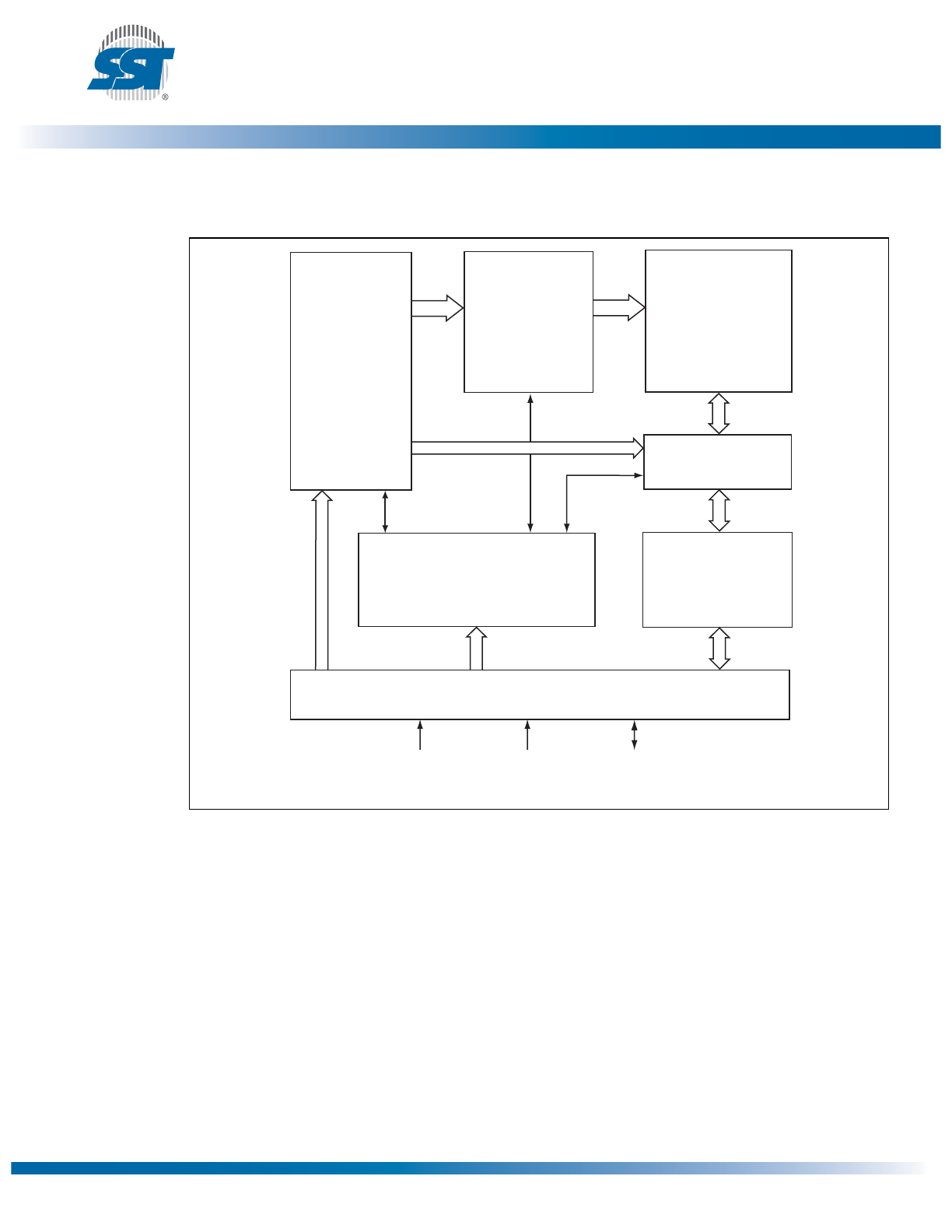
Block Diagram
Figure 1: Functional Block Diagram
1359 B1.0
Page Buffer,
I/O Buffers
and
Data Latches
SuperFlash
Memory
X - Decoder
Control Logic
Address
Buffers
and
Latches
CE#
Y - Decoder
SCK
SIO [3:0]
Serial Interface
©2011 Silicon Storage Technology, Inc.
DS-25017A
04/11
4
Serial Quad I/O (SQI) Flash Memory
SST26VF016 / SST26VF032
Data Sheet
A Microchip Technology Company
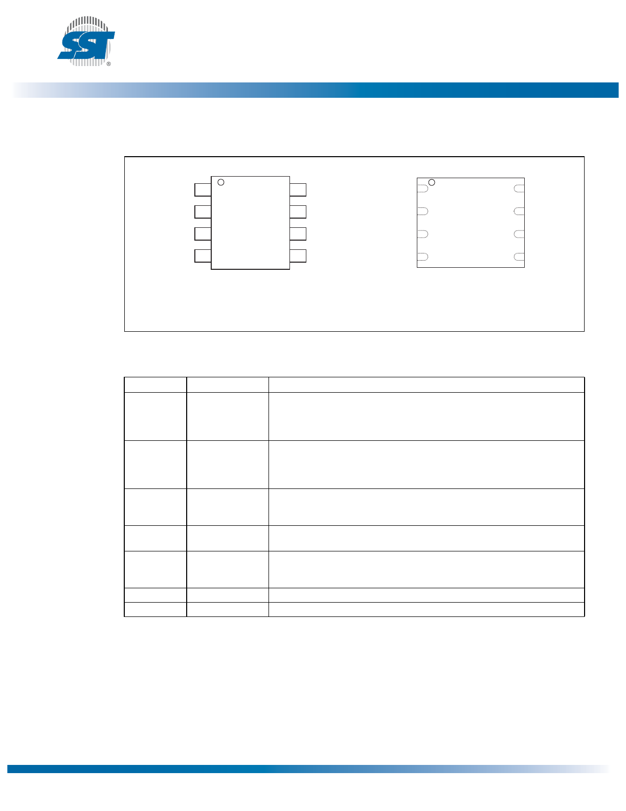
Pin Description
Figure 2: Pin Description for 8-lead SOIC and 8-contact WSON
Table 1: Pin Description
Symbol
Pin Name
Functions
SCK
Serial Clock
To provide the timing of the serial interface.
Commands, addresses, or input data are latched on the rising edge of the
clock input, while output data is shifted out on the falling edge of the clock
input.
SIO[3:0]
Serial Data
Input/Output
To transfer commands, addresses, or data serially into the device or data out
of the device. Inputs are latched on the rising edge of the serial clock. Data is
shifted out on the falling edge of the serial clock. The EQIO command
instruction configures these pins for Quad I/O mode.
SI
Serial Data Input
for SPI mode
To transfer commands, addresses or data serially into the device. Inputs are
latched on the rising edge of the serial clock. SI is the default state after a
power on reset.
SO
Serial Data Output
for SPI mode
To transfer data serially out of the device. Data is shifted out on the falling
edge of the serial clock. SO is the default state after a power on reset.
CE#
Chip Enable
The device is enabled by a high to low transition on CE#. CE# must remain
low for the duration of any command sequence; or in the case of Write oper-
ations, for the command/data input sequence.
V
DD
Power Supply
To provide power supply voltage: 2.7-3.6V
V
SS
Ground
T1.0 25017
1
2
3
4
8
7
6
5
CE#
SO/SIO1
SIO2
VSS
VDD
SIO3
SCK
SI/SIO0
Top View
1359 08-soic S2A P1.0
1
2
3
4
8
7
6
5
CE#
SO/SIO1
SIO2
VSS
Top View
VDD
SIO3
SCK
SI/SIO0
1359 08-wson QA P1.0
8-Lead SOIC
8-Contact WSON
©2011 Silicon Storage Technology, Inc.
DS-25017A
04/11
5
Serial Quad I/O (SQI) Flash Memory
SST26VF016 / SST26VF032
Data Sheet
A Microchip Technology Company
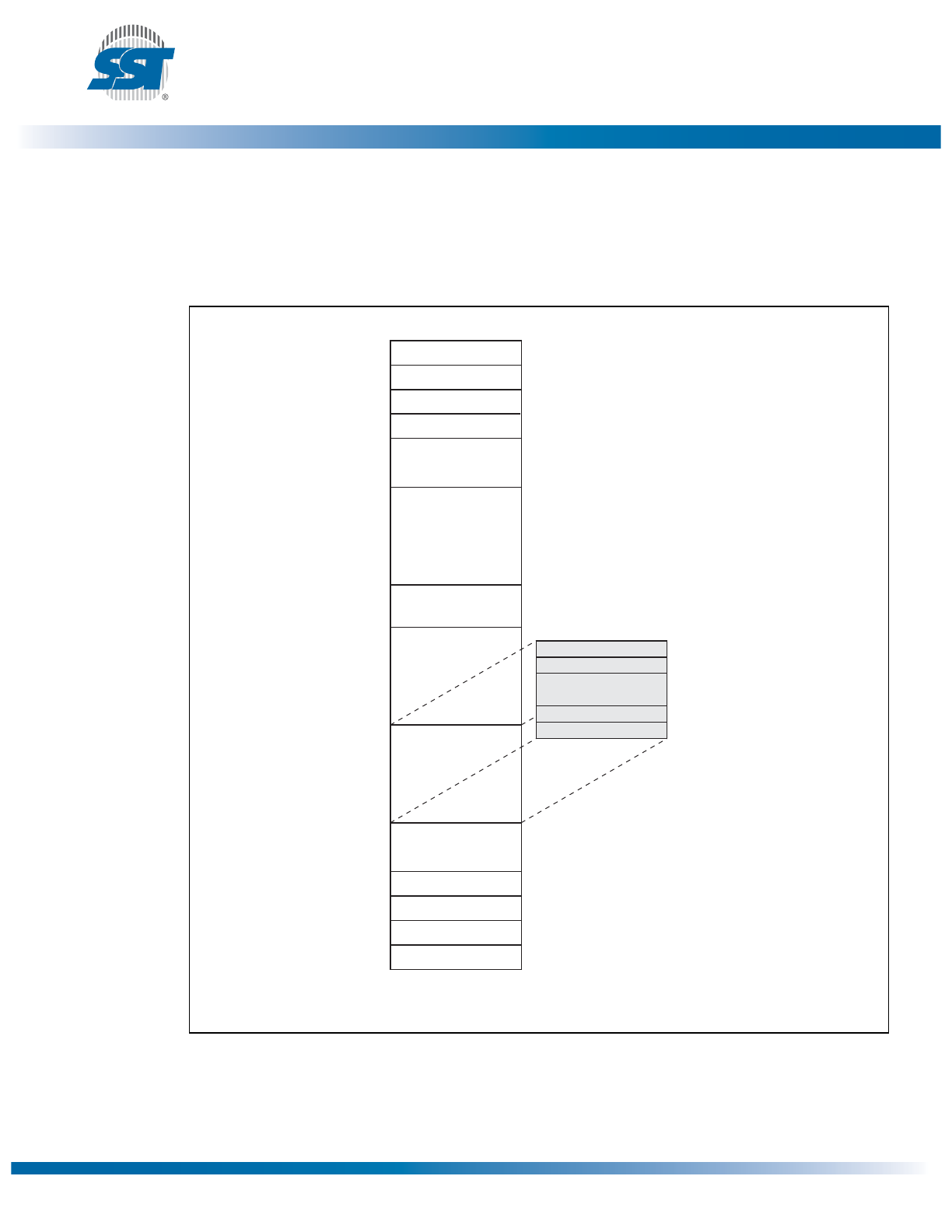
Memory Organization
The SST26VF016/032 SQI memory array is organized in uniform 4 KByte erasable sectors with eight
8 KByte parameters. In addition, the array also includes two 32 KByte and 30/62 64 KByte erasable
overlay blocks. See Figure 3.
Figure 3: Memory Map
1359 F41.0
Top of Memory Block
8 KByte
8 KByte
8 KByte
8 KByte
32 KByte
64 KByte
64 KByte
64 KByte
32 KByte
8 KByte
8 KByte
8 KByte
8 KByte
Bottom of Memory Block
4 KByte
4 KByte
4 KByte
4 KByte
. . .
2 Sectors for 8 KByte blocks
8 Sectors for 32 KByte blocks
16 Sectors for 64 KByte blocks
. . .
©2011 Silicon Storage Technology, Inc.
DS-25017A
04/11
6
Serial Quad I/O (SQI) Flash Memory
SST26VF016 / SST26VF032
Data Sheet
A Microchip Technology Company
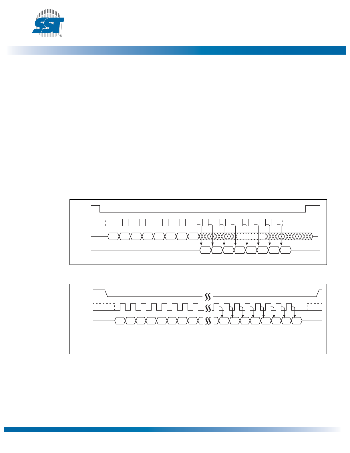
Device Operation
The SST26VF016/032 supports both Serial Peripheral Interface (SPI) bus protocol and the new 4-bit
multiplexed Serial Quad I/O (SQI) bus protocol. To provide backward compatibility to traditional SPI
Serial Flash devices, the device’s initial state after a power-on reset is SPI bus protocol supporting only
Read, High Speed Read, and JEDEC-ID Read instructions. A command instruction configures the
device to Serial Quad I/O bus protocol. The dataflow in this bus protocol is controlled with four multi-
plexed I/O signals, a chip enable (CE#), and serial clock (SCK).
SQI Flash Memory protocol supports both Mode 0 (0,0) and Mode 3 (1,1) bus operations. The differ-
ence between the two modes, as shown in Figures 4 and 5, is the state of the SCK signal when the
bus master is in Stand-by mode and no data is being transferred. The SCK signal is low for Mode 0
and SCK signal is high for Mode 3. For both modes, the Serial Data I/O (SIO[3:0]) is sampled at the ris-
ing edge of the SCK clock signal for input, and driven after the falling edge of the SCK clock signal for
output. The traditional SPI protocol uses separate input (SI) and output (SO) data signals as shown in
Figure 4. The SST26VF016/032 use four multiplexed signals, SIO[3:0], for both data in and data out,
as shown in Figure 5. This quadruples the traditional bus transfer speed at the same clock frequency,
without the need for more pins on the package.
Figure 4: SPI Protocol (Traditional 25 Serial SPI Device)
Figure 5: SQI Serial Quad I/O Protocol
1359 F03.0
MODE 3
SCK
SI
SO
CE#
MODE 3
DON T CARE
Bit 7 Bit 6 Bit 5 Bit 4 Bit 3 Bit 2 Bit 1 Bit 0
Bit 7 Bit 6 Bit 5 Bit 4 Bit 3 Bit 2 Bit 1 Bit 0
MODE 0
MODE 0
HIGH IMPEDANCE
MSB
MSB
1409 F04.1
MODE 3
CLK
SIO(3:0)
CE#
MODE 3
C1
C0
A5
A4
A3
A2
A1
A0
H0
L0
H1
L1
H2
L2
H3
L3
MODE 0
MODE 0
MSB
X = Don’t Care or High Impediance
©2011 Silicon Storage Technology, Inc.
DS-25017A
04/11
7
Serial Quad I/O (SQI) Flash Memory
SST26VF016 / SST26VF032
Data Sheet
A Microchip Technology Company
Device Protection
The SST26VF016/032 have a Block-Protection register which provides a software mechanism to write-
lock the array and write-lock, and/or read-lock, the parameter blocks. The Block-Protection Register is
48/80 bits wide per device: two bits each for the eight 8 KByte parameter blocks (write-lock and read-
lock), and one bit each for the remaining 32 KByte and 64 KByte overlay blocks (write-lock). See
Tables 8 - 9 for address range protected per register bit.
Each bit in the Block-Protection Register can be written to a ‘1’ (protected) or ‘0’ (unprotected). For the
parameter blocks, the most significant bit is for read-lock, and the least significant bit is for write-lock. Read-
locking the parameter blocks provides additional security for sensitive data after retrieval (e.g., after initial
boot). If a block is read-locked all reads to the block return data 00H. All blocks are write-locked and read-
unlocked after power-up or reset. The Write Block Locking Register command is a two cycle command
requiring Write-Enable (WREN) to be executed prior to the Write Block-Protection Register command.
Figure 6: Block Locking Memory Map
1359 F40.2
Top of Memory Block
8 KByte
8 KByte
8 KByte
8 KByte
32 KByte
64 KByte
64 KByte
64 KByte
32 KByte
8 KByte
8 KByte
8 KByte
8 KByte
Read Lock
Write Lock
Read Lock
Write Lock
Write Lock
Bottom of Memory Block
. . .

©2011 Silicon Storage Technology, Inc.
DS-25017A
04/11
8
Serial Quad I/O (SQI) Flash Memory
SST26VF016 / SST26VF032
Data Sheet
A Microchip Technology Company
Write-Protection Lock-Down
To prevent changes, the Block-Protection register can be set to Write-Protection Lock-Down using the
Lock Down Block Protection Register (LPBR) command. Once the Write-Protection Lock-Down is
enabled, the Block-Protection register can not be changed. To avoid inadvertent lock down, the WREN
command must be executed prior to the LBPR command.
To reset Write-Protection Lock-Down, power cycle the device. The Write-Protection Lock-Down status
may be read from the Status register.
Security ID
SST26VF016/032 offer a 256-bit Security ID (Sec ID) feature. The Security ID space is divided into two
parts – one factory-programmed, 64-bit segment and one user-programmable 192-bit segment. The
factory-programmed segment is programmed at SST with a unique number and cannot be changed.
The user-programmable segment is left unprogrammed for the customer to program as desired.
Use the SecID Program command to program the Security ID using the address shown in Table 7.
Once programmed, the Security ID can be locked using the Lockout Sec ID command. This prevents
any future write to the Security ID.
The factory-programmed portion of the Security ID can’t be programmed by the user; neither factory-
programmed nor user-programmable areas can be erased.
©2011 Silicon Storage Technology, Inc.
DS-25017A
04/11
9
Serial Quad I/O (SQI) Flash Memory
SST26VF016 / SST26VF032
Data Sheet
A Microchip Technology Company
Status Register
The Status register is a read-only register that provides status on whether the flash memory array is
available for any Read or Write operation, whether the device is Write enabled, and whether an erase
or program operation is suspended. During an internal Erase or Program operation, the Status register
may be read to determine the completion of an operation in progress. Table 2 describes the function of
each bit in the Status register.
Table 2: Status Register
Bit
Name
Function
Default at
Power-up
0
RES
Reserved for future use
0
1
WEL
Write-Enable Latch status
1 = Device is memory Write enabled
0 = Device is not memory Write enabled
0
2
WSE
Write Suspend-Erase status
1 = Erase suspended
0 = Erase is not suspended
0
3
WSP
Write Suspend-Program status
1 = Program suspended
0 = Program is not suspended
0
4
WPLD
Write Protection Lock-Down status
1 = Write Protection Lock-Down enabled
0 = Write Protection Lock-Down disabled
0
5
SEC
1
1. The Security ID status will always be ‘1’ at power-up after a successful execution of the Lockout Sec ID instruction, oth-
erwise default at power-up is ‘0’.
Security ID status
1 = Security ID space locked
0 = Security ID space not locked
0
1
6
RES
Reserved for future use
0
7
BUSY
Write operation status
1 = Internal Write operation is in progress
0 = No internal Write operation is in progress
0
T2.0 25017

©2011 Silicon Storage Technology, Inc.
DS-25017A
04/11
10
Serial Quad I/O (SQI) Flash Memory
SST26VF016 / SST26VF032
Data Sheet
A Microchip Technology Company
Write-Enable Latch (WEL)
The Write-Enable Latch (WEL) bit indicates the status of the internal memory’s Write-Enable Latch. If
the WEL bit is set to ‘1’, the device is write enabled. If the bit is set to ‘0’ (reset), the device is not write
enabled and does not accept any memory Program or Erase, Protection Register Write, or Lock-Down
commands. The Write-Enable Latch bit is automatically reset under the following conditions:
•
Power-up
•
Reset
•
Write-Disable (WRDI) instruction completion
•
Page-Program instruction completion
•
Sector-Erase instruction completion
•
Block-Erase instruction completion
•
Chip-Erase instruction completion
•
Write-Block-Protection register instruction
•
Lock-Down Block-Protection register instruction
•
Program Security ID instruction completion
•
Lockout Security ID instruction completion
•
Write-Suspend instruction
Write Suspend Erase Status (WSE)
The Write Suspend-Erase Status (WSE) indicates when an Erase operation has been suspended. The
WSE bit is ‘1’ after the host issues a suspend command during an Erase operation. Once the sus-
pended Erase resumes, the WSE bit is reset to ‘0.’
Write Suspend Program Status (WSP)
The Write Suspend-Program Status (WSP) bit indicates when a Program operation has been sus-
pended. The WSP is ‘1’ after the host issues a suspend command during the Program operation. Once
the suspended Program resumes, the WSP bit is reset to ‘0.’
Write Protection Lockdown Status (WPLD)
The Write Protection-Lockdown Status (WPLD) bit indicates when the Block Protection register is
locked-down to prevent changes to the protection settings. The WPLD is ‘1’ after the host issues a
Lock-Down Block Protection command. After a power cycle, the WPLD bit is reset to ‘0.’
Security ID Status (SEC)
The Security ID Status (SEC) bit indicates when the Security ID space is locked to prevent a Write
command. The SEC is ‘1’ after the host issues a Lockout SID command. Once the host issues a Lock-
out SID command, the SEC bit can never be reset to ‘0.’
Busy
The Busy bit determines whether there is an internal Erase or Program operation in progress. If the
BUSY bit is ‘1’, the device is busy with an internal Erase or Program operation. If the bit is ‘0’, no Erase
or Program operation is in progress.