
© 2011 Microchip Technology Inc.
DS22049F-page 1
MCP1703
Features:
• 2.0 µA Typical Quiescent Current
• Input Operating Voltage Range: 2.7V to16.0V
• 250 mA Output Current for Output Voltages
≥ 2.5V
• 200 mA Output Current for Output Voltages < 2.5V
• Low Dropout Voltage, 625 mV typical @ 250 mA
for V
R
= 2.8V
• 0.4% Typical Output Voltage Tolerance
• Standard Output Voltage Options:
- 1.2V, 1.5V, 1.8V, 2.5V, 2.8V, 3.0V, 3.3V, 4.0V,
5.0V
• Output Voltage Range: 1.2V to 5.5V in 0.1V
Increments (50 mV increments available upon
request)
• Stable with 1.0 µF to 22 µF Ceramic Output
Capacitance
• Short-Circuit Protection
• Overtemperature Protection
Applications:
• Battery-Powered Devices
• Battery-Powered Alarm Circuits
• Smoke Detectors
• CO
2
Detectors
• Pagers and Cellular Phones
• Smart Battery Packs
• Low Quiescent Current Voltage Reference
• PDAs
• Digital Cameras
• Microcontroller Power
• Solar-Powered Instruments
• Consumer Products
• Battery-Powered Data Loggers
Related Literature:
• AN765, “Using Microchip’s Micropower LDOs”,
DS00765, Microchip Technology Inc., 2002
• AN766, “Pin-Compatible CMOS Upgrades to
Bipolar LDOs”, DS00766,
Microchip Technology Inc., 2002
• AN792, “A Method to Determine How Much
Power a SOT23 Can Dissipate in an Application”,
DS00792, Microchip Technology Inc., 2001
Description:
The MCP1703 is a family of CMOS low dropout (LDO)
voltage regulators that can deliver up to 250 mA of
current while consuming only 2.0 µA of quiescent
current (typical). The input operating range is specified
from 2.7V to 16.0V, making it an ideal choice for two to
six primary cell battery-powered applications, 9V
alkaline and one or two cell Li-Ion-powered
applications.
The MCP1703 is capable of delivering 250 mA with
only 625 mV (typical) of input to output voltage
differential (V
OUT
= 2.8V). The output voltage tolerance
of the MCP1703 is typically ±0.4% at +25°C and ±3%
maximum over the operating junction temperature
range of -40°C to +125°C. Line regulation is ±0.1%
typical at +25°C.
Output voltages available for the MCP1703 range from
1.2V to 5.5V. The LDO output is stable when using only
1 µF of output capacitance. Ceramic, tantalum, or
aluminum electrolytic capacitors can all be used for
input and output. Overcurrent limit and overtemperature
shutdown provide a robust solution for any application.
Package options include the SOT-223-3, SOT-23A,
2x3 DFN-8, and SOT-89-3.
Package Types
1
3
2
V
IN
GND V
OUT
1
2
3
V
IN
GND
V
OUT
3-Pin SOT-23A
3-Pin SOT-89
V
IN
1
2
3
SOT-223-3
GND
V
IN
V
OUT
NC
NC
GND
NC
NC
1
2
3
4
8
7
6
5 NC
V
OUT
EP
9
* Includes Exposed Thermal Pad (EP); see
Table 3-1
.
V
IN
2x3 DFN-8 *
250 mA, 16V, Low Quiescent Current LDO Regulator
MCP1703
DS22049F-page 2
© 2011 Microchip Technology Inc.
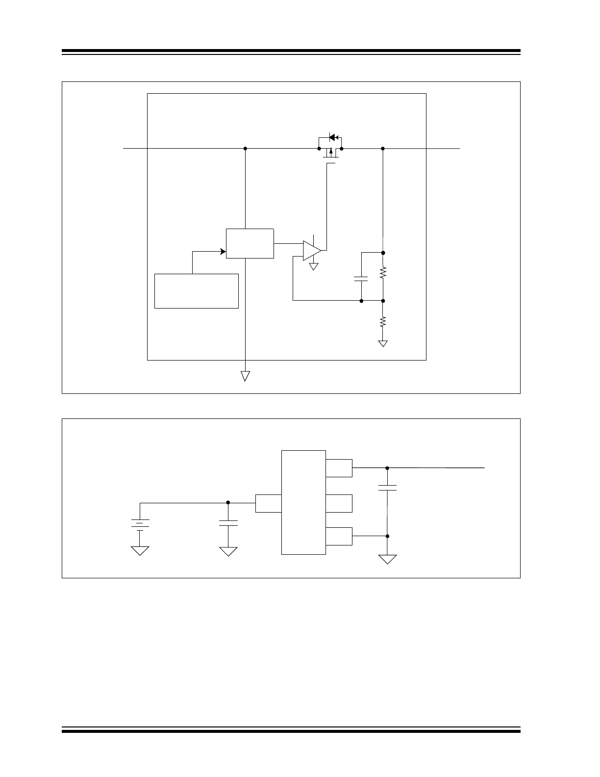
Functional Block Diagrams
Typical Application Circuits
+
-
MCP1703
V
IN
V
OUT
GND
+V
IN
Error Amplifier
Voltage
Reference
Overcurrent
Overtemperature
MCP1703
V
IN
C
IN
1 µF Ceramic
C
OUT
1 µF Ceramic
V
OUT
V
IN
3.3V
I
OUT
50 mA
V
IN
V
OUT
9V
Battery
+
GND
© 2011 Microchip Technology Inc.
DS22049F-page 3
MCP1703
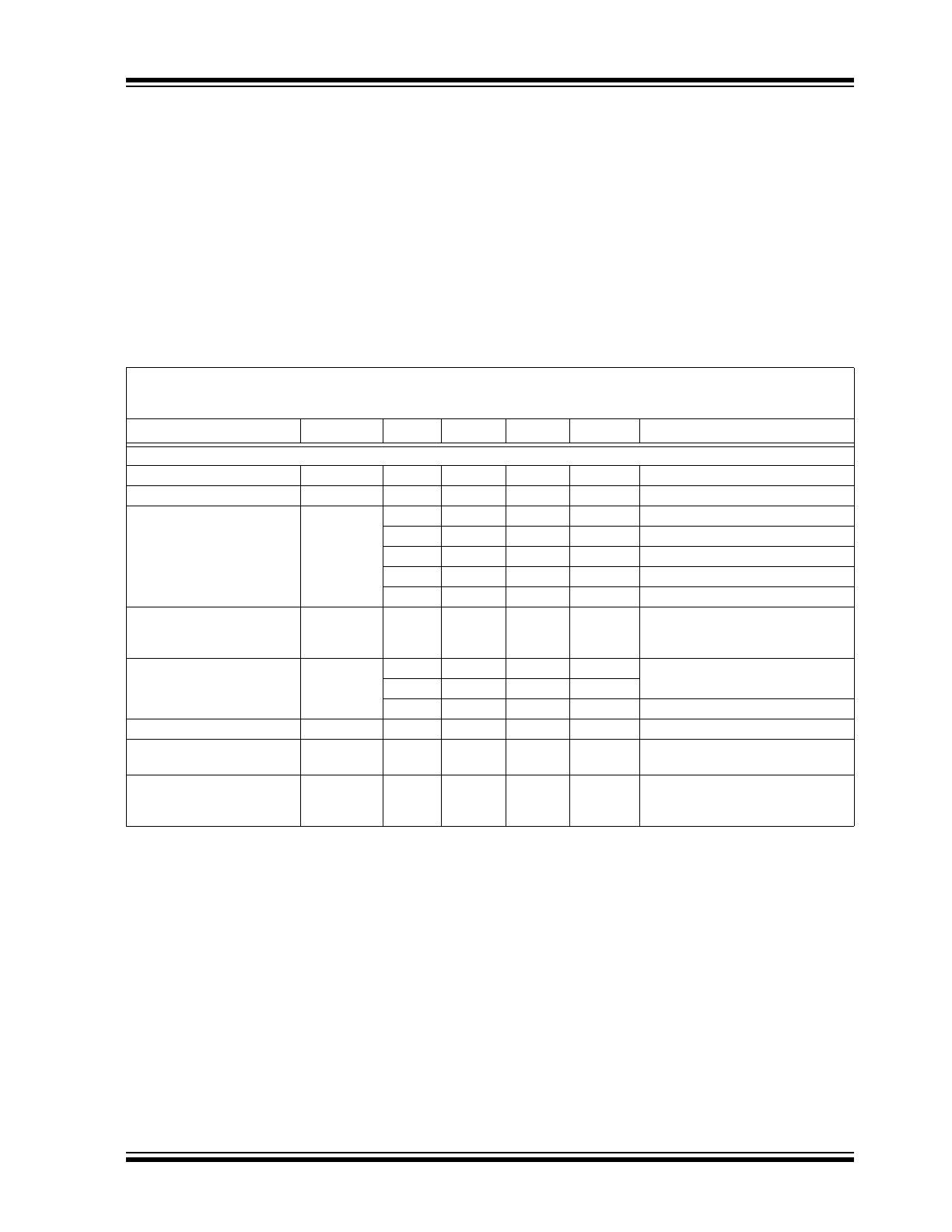
1.0
ELECTRICAL
CHARACTERISTICS
Absolute Maximum Ratings †
V
DD
..................................................................................+18V
All inputs and outputs w.r.t. .............(V
SS
-0.3V) to (V
IN
+0.3V)
Peak Output Current ...................................................500 mA
Storage temperature .....................................-65°C to +150°C
Maximum Junction Temperature ................................. +150°C
ESD protection on all pins (HBM;MM)
............... ≥ 4 kV; ≥ 400V
† Notice: Stresses above those listed under “Maximum
Ratings” may cause permanent damage to the device. This is
a stress rating only and functional operation of the device at
those or any other conditions above those indicated in the
operational listings of this specification is not implied.
Exposure to maximum rating conditions for extended periods
may affect device reliability.
DC CHARACTERISTICS
Electrical Specifications: Unless otherwise specified, all limits are established for V
IN
= V
OUT(MAX)
+ V
DROPOUT(MAX)
,
Note 1
,
I
LOAD
= 100 µA, C
OUT
= 1 µF (X7R), C
IN
= 1 µF (X7R), T
A
= +25°C.
Boldface type applies for junction temperatures, T
J
(
Note 7
) of -40°C to +125°C.
Parameters
Symbol
Min
Typ
Max
Units
Conditions
Input / Output Characteristics
Input Operating Voltage
V
IN
2.7
—
16.0
V
Note 1
Input Quiescent Current
I
q
—
2.0
5
µA
I
L
= 0 mA
Maximum Output Current
I
OUT_mA
250
—
—
mA
For V
R
≥ 2.5V
50
100
—
mA
For V
R
< 2.5V, V
IN
≥ 2.7V
100
130
—
mA
For V
R
< 2.5V, V
IN
≥ 2.95V
150
200
—
mA
For V
R
< 2.5V, V
IN
≥ 3.2V
200
250
—
mA
For V
R
< 2.5V, V
IN
≥ 3.45V
Output Short Circuit Current
I
OUT_SC
—
400
—
mA
V
IN
= V
IN(MIN)
(
Note 1
), V
OUT
= GND,
Current (average current) measured
10 ms after short is applied.
Output Voltage Regulation
V
OUT
V
R
-3.0% V
R
±0.4%
V
R
+3.0%
V
Note 2
V
R
-2.0%
V
R
±0.4%
V
R
+2.0%
V
V
R
-1.0%
V
R
±0.4%
V
R
+1.0%
V
1% Custom
V
OUT
Temperature Coefficient
TCV
OUT
—
50
—
ppm/°C
Note 3
Line Regulation
ΔV
OUT
/
(V
OUT
X
ΔV
IN
)
-0.3
±0.1
+0.3
%/V
(V
OUT(MAX)
+ V
DROPOUT(MAX)
)
≤ V
IN
≤ 16V,
Note 1
Load Regulation
Δ
V
OUT
/V
OUT
-2.5
±1.0
+2.5
%
I
L
= 1.0 mA to 250 mA for V
R
>= 2.5V
I
L
= 1.0 mA to 200 mA for V
R
< 2.5V
V
IN
= 3.65V,
Note 4
Note 1:
The minimum V
IN
must meet two conditions: V
IN
≥ 2.7V and V
IN
≥ (V
OUT(MAX)
+ V
DROPOUT(MAX)
).
2:
V
R
is the nominal regulator output voltage. For example: V
R
= 1.2V, 1.5V, 1.8V, 2.5V, 2.8V, 3.0V, 3.3V, 4.0V, or 5.0V.
The input voltage V
IN
= V
OUT(MAX)
+ V
DROPOUT(MAX)
or Vi
IN
= 2.7V (whichever is greater); I
OUT
= 100 µA.
3:
TCV
OUT
= (V
OUT-HIGH
- V
OUT-LOW
) *10
6
/ (V
R
*
ΔTemperature), V
OUT-HIGH
= highest voltage measured over the
temperature range. V
OUT-LOW
= lowest voltage measured over the temperature range.
4:
Load regulation is measured at a constant junction temperature using low duty cycle pulse testing. Changes in output
voltage due to heating effects are determined using thermal regulation specification TCV
OUT
.
5:
Dropout voltage is defined as the input to output differential at which the output voltage drops 2% below its measured
value with an applied input voltage of V
OUT(MAX)
+ V
DROPOUT(MAX)
or 2.7V, whichever is greater.
6:
The maximum allowable power dissipation is a function of ambient temperature, the maximum allowable junction
temperature and the thermal resistance from junction to air (i.e., T
A
, T
J
,
θ
JA
). Exceeding the maximum allowable power
dissipation will cause the device operating junction temperature to exceed the maximum 150°C rating. Sustained
junction temperatures above 150°C can impact the device reliability.
7:
The junction temperature is approximated by soaking the device under test at an ambient temperature equal to the
desired junction temperature. The test time is small enough such that the rise in the junction temperature over the
ambient temperature is not significant.
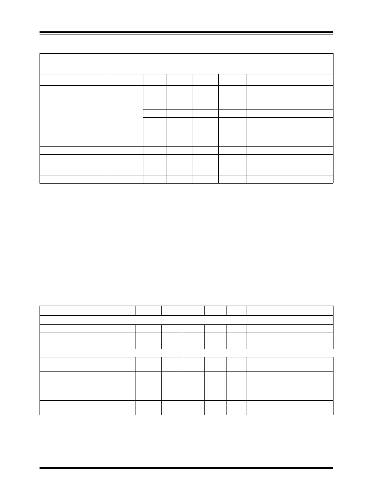
MCP1703
DS22049F-page 4
© 2011 Microchip Technology Inc.
TEMPERATURE SPECIFICATIONS
(
1
)
Dropout Voltage
Note 1
,
Note 5
V
DROPOUT
—
330
650
mV
I
L
= 250 mA, V
R
= 5.0V
—
525
725
mV
I
L
= 250 mA, 3.3V
≤ V
R
< 5.0V
—
625
975
mV
I
L
= 250 mA, 2.8V
≤ V
R
< 3.3V
—
750
1100
mV
I
L
= 250 mA, 2.5V
≤ V
R
< 2.8V
—
—
—
mV
V
R
< 2.5V, See Maximum Output
Current Parameter
Output Delay Time
T
DELAY
—
1000
—
µs
V
IN
= 0V to 6V, V
OUT
= 90% V
R
,
R
L
= 50
Ω resistive
Output Noise
e
N
—
8
µV/(Hz)
1/2
I
L
= 50 mA, f = 1 kHz, C
OUT
= 1 µF
Power Supply Ripple
Rejection Ratio
PSRR
—
44
—
dB
f = 100 Hz, C
OUT
= 1 µF, I
L
= 100 µA,
V
INAC
= 100 mV pk-pk, C
IN
= 0 µF,
V
R
= 1.2V
Thermal Shutdown Protection
T
SD
—
150
—
°C
Parameters
Sym
Min
Typ
Max
Units
Conditions
Temperature Ranges
Operating Junction Temperature Range
T
J
-40
—
+125
°C
Steady State
Maximum Junction Temperature
T
J
—
—
+150
°C
Transient
Storage Temperature Range
T
A
-65
—
+150
°C
Thermal Package Resistance (
Note 2
)
Thermal Resistance, 3LD SOT-223
θ
JA
θ
JC
—
—
62
15
—
—
°C/W
EIA/JEDEC JESD51-7
FR-4 0.063 4-Layer Board
Thermal Resistance, 3LD SOT-23A
θ
JA
θ
JC
—
—
336
110
—
—
°C/W
EIA/JEDEC JESD51-7
FR-4 0.063 4-Layer Board
Thermal Resistance, 3LD SOT-89
θ
JA
θ
JC
—
—
153,3
100
—
—
°C/W
EIA/JEDEC JESD51-7
FR-4 0.063 4-Layer Board
Thermal Resistance, 8LD 2x3 DFN
θ
JA
θ
JC
—
—
93
26
—
—
°C/W
EIA/JEDEC JESD51-7
FR-4 0.063 4-Layer Board
Note 1: The maximum allowable power dissipation is a function of ambient temperature, the maximum allowable junction
temperature and the thermal resistance from junction to air (i.e., T
A
, T
J
,
θ
JA
). Exceeding the maximum allowable power
dissipation will cause the device operating junction temperature to exceed the maximum 150°C rating. Sustained
junction temperatures above 150°C can impact the device reliability.
2: Thermal Resistance values are subject to change. Please visit the Microchip web site for the latest packaging
information.
DC CHARACTERISTICS (CONTINUED)
Electrical Specifications: Unless otherwise specified, all limits are established for V
IN
= V
OUT(MAX)
+ V
DROPOUT(MAX)
,
Note 1
,
I
LOAD
= 100 µA, C
OUT
= 1 µF (X7R), C
IN
= 1 µF (X7R), T
A
= +25°C.
Boldface type applies for junction temperatures, T
J
(
Note 7
) of -40°C to +125°C.
Parameters
Symbol
Min
Typ
Max
Units
Conditions
Note 1:
The minimum V
IN
must meet two conditions: V
IN
≥ 2.7V and V
IN
≥ (V
OUT(MAX)
+ V
DROPOUT(MAX)
).
2:
V
R
is the nominal regulator output voltage. For example: V
R
= 1.2V, 1.5V, 1.8V, 2.5V, 2.8V, 3.0V, 3.3V, 4.0V, or 5.0V.
The input voltage V
IN
= V
OUT(MAX)
+ V
DROPOUT(MAX)
or Vi
IN
= 2.7V (whichever is greater); I
OUT
= 100 µA.
3:
TCV
OUT
= (V
OUT-HIGH
- V
OUT-LOW
) *10
6
/ (V
R
*
ΔTemperature), V
OUT-HIGH
= highest voltage measured over the
temperature range. V
OUT-LOW
= lowest voltage measured over the temperature range.
4:
Load regulation is measured at a constant junction temperature using low duty cycle pulse testing. Changes in output
voltage due to heating effects are determined using thermal regulation specification TCV
OUT
.
5:
Dropout voltage is defined as the input to output differential at which the output voltage drops 2% below its measured
value with an applied input voltage of V
OUT(MAX)
+ V
DROPOUT(MAX)
or 2.7V, whichever is greater.
6:
The maximum allowable power dissipation is a function of ambient temperature, the maximum allowable junction
temperature and the thermal resistance from junction to air (i.e., T
A
, T
J
,
θ
JA
). Exceeding the maximum allowable power
dissipation will cause the device operating junction temperature to exceed the maximum 150°C rating. Sustained
junction temperatures above 150°C can impact the device reliability.
7:
The junction temperature is approximated by soaking the device under test at an ambient temperature equal to the
desired junction temperature. The test time is small enough such that the rise in the junction temperature over the
ambient temperature is not significant.
© 2011 Microchip Technology Inc.
DS22049F-page 5
MCP1703
2.0
TYPICAL PERFORMANCE CURVES
Note: Unless otherwise indicated: V
R
= 1.8V, C
OUT
= 1 µF Ceramic (X7R), C
IN
= 1 µF Ceramic (X7R), I
L
= 100 µA,
T
A
= +25°C, V
IN
= V
OUT(MAX)
+ V
DROPOUT(MAX)
or 2.7V, whichever is greater.
Note: Junction Temperature (T
J
) is approximated by soaking the device under test to an ambient temperature equal to the desired junction
temperature. The test time is small enough such that the rise in Junction temperature over the Ambient temperature is not significant.
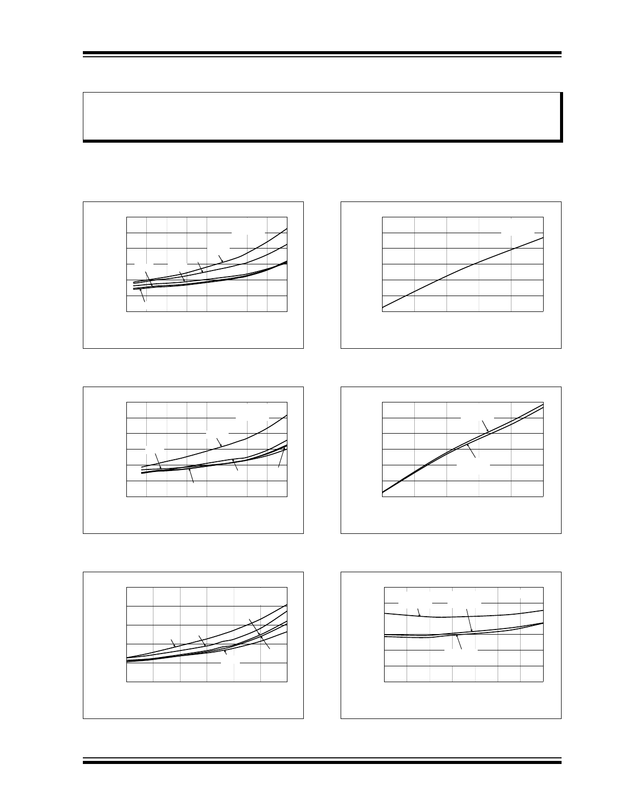
FIGURE 2-1:
Quiescent Current vs. Input
Voltage.
FIGURE 2-2:
Quiescent Current vs. Input
Voltage.
FIGURE 2-3:
Quiescent Current vs. Input
Voltage.
FIGURE 2-4:
Ground Current vs. Load
Current.
FIGURE 2-5:
Ground Current vs. Load
Current.
FIGURE 2-6:
Quiescent Current vs.
Junction Temperature.
Note:
The graphs and tables provided following this note are a statistical summary based on a limited number of
samples and are provided for informational purposes only. The performance characteristics listed herein
are not tested or guaranteed. In some graphs or tables, the data presented may be outside the specified
operating range (e.g., outside specified power supply range) and therefore outside the warranted range.
0.00
1.00
2.00
3.00
4.00
5.00
6.00
2
4
6
8
10
12
14
16
18
Input Voltage (V)
Qu
ie
sc
e
n
t Cu
rre
n
t (
µ
A)
V
OUT
= 1.2V
I
OUT
= 0 µA
+25°C
+130°C
-45°C
0°C
+90°C
0.00
1.00
2.00
3.00
4.00
5.00
6.00
2
4
6
8
10
12
14
16
18
Input Voltage (V)
Quie
s
c
ent C
u
rr
en
t (µA)
V
OUT
= 2.5V
I
OUT
= 0 µA
+25°C
+130°C
-45°C
0°C
+90°C
1.00
2.00
3.00
4.00
5.00
6.00
6
8
10
12
14
16
18
Input Voltage (V)
Q
u
iesc
en
t C
u
rr
ent
(
µ
A
)
V
OUT
= 5.0V
I
OUT
= 0 µA
+25°C
+130°C
-45°C
0°C
+90°C
0
20
40
60
80
100
120
0
40
80
120
160
200
Load Current (mA)
GND Cu
rre
n
t (µ
A
)
V
OUT
= 1.2V
V
IN
= 2.7V
0
20
40
60
80
100
120
0
50
100
150
200
250
Load Current (mA)
GND
Cu
rre
n
t (µ
A)
V
OUT
= 5.0V
V
IN
= 6.0V
V
OUT
= 2.5V
V
IN
= 3.5V
0.00
0.50
1.00
1.50
2.00
2.50
3.00
-45
-20
5
30
55
80
105
130
Junction Temperature (°C)
Q
u
ie
sc
ent
C
u
rr
e
n
t (
µ
A
)
I
OUT
= 0 mA
V
OUT
= 5.0V
V
IN
= 6.0V
V
OUT
= 1.2V
V
IN
= 2.7V
V
OUT
= 2.5V
V
IN
= 3.5V
MCP1703
DS22049F-page 6
© 2011 Microchip Technology Inc.
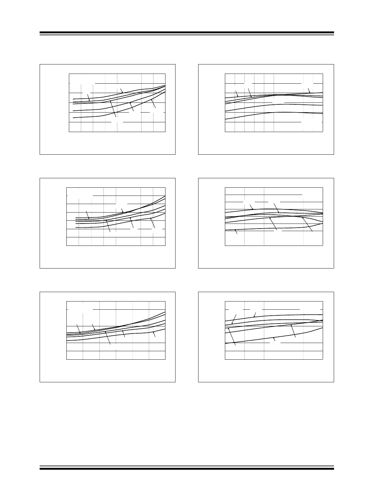
Note: Unless otherwise indicated: V
R
= 1.8V, C
OUT
= 1 µF Ceramic (X7R), C
IN
= 1 µF Ceramic (X7R), I
L
= 100 µA,
T
A
= +25°C, V
IN
= V
OUT(MAX)
+ V
DROPOUT(MAX)
or 2.7V, whichever is greater.
FIGURE 2-7:
Output Voltage vs. Input
Voltage.
FIGURE 2-8:
Output Voltage vs. Input
Voltage.
FIGURE 2-9:
Output Voltage vs. Input
Voltage.
FIGURE 2-10:
Output Voltage vs. Load
Current.
FIGURE 2-11:
Output Voltage vs. Load
Current.
FIGURE 2-12:
Output Voltage vs. Load
Current.
1.180
1.190
1.200
1.210
1.220
1.230
1.240
2
4
6
8
10
12
14
16
18
Input Voltage (V)
O
u
tput Volta
g
e (V)
V
OUT
= 1.2V
I
LOAD
= 0.1 mA
+25°C
+130°C
-45°C
0°C
+90°C
2.44
2.46
2.48
2.50
2.52
2.54
2.56
2.58
2
4
6
8
10
12
14
16
18
Input Voltage (V)
Outpu
t Vol
ta
g
e (V)
V
OUT
= 2.5V
I
LOAD
= 0.1 mA
+25°C
+130°C
-45°C
0°C
+90°C
4.88
4.92
4.96
5.00
5.04
5.08
5.12
5.16
6
8
10
12
14
16
18
Input Voltage (V)
O
u
tput Volta
g
e (V)
V
OUT
= 5.0V
I
LOAD
= 0.1 mA
+25°C
+130°C
-45°C
0°C
+90°C
1.18
1.19
1.20
1.21
1.22
1.23
1.24
0
20
40
60
80 100 120 140 160 180 200
Load Current (mA)
O
u
tput Volta
g
e (V)
V
IN
= 3.0V
V
OUT
= 1.2V
+25°C
+130°C
-45°C
0°C
+90°C
2.46
2.47
2.48
2.49
2.50
2.51
2.52
2.53
2.54
0
50
100
150
200
250
Load Current (mA)
O
u
tput Volta
g
e (V)
V
IN
= 3.5V
V
OUT
= 2.5V
+25°C
+130°C
-45°C
0°C
+90°C
4.92
4.94
4.96
4.98
5.00
5.02
5.04
5.06
0
50
100
150
200
250
Load Current (mA)
O
u
tput
Volt
age
(V)
V
IN
= 6V
V
OUT
= 5.0V
+25°C
+130°C
-45°C
0°C
+90°C
© 2011 Microchip Technology Inc.
DS22049F-page 7
MCP1703
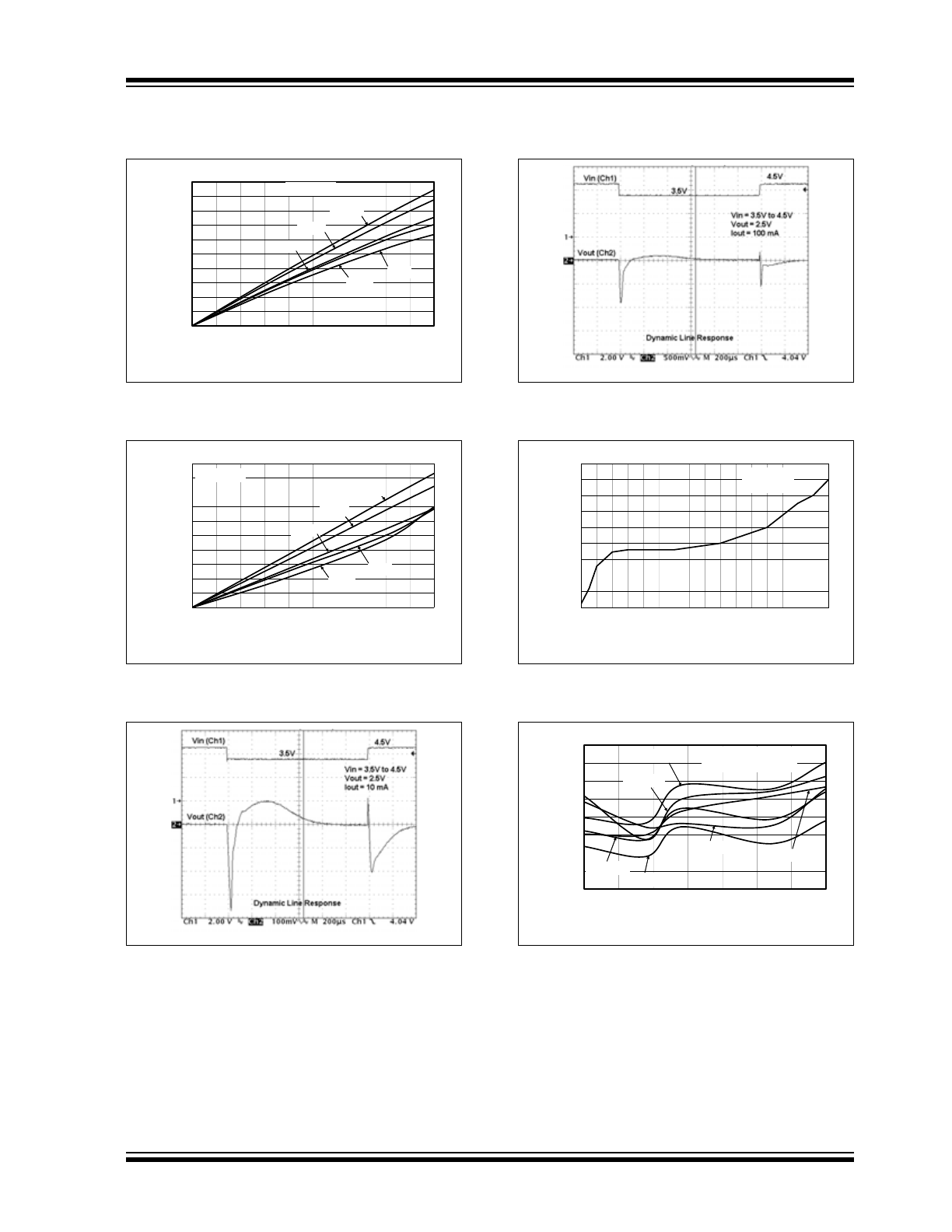
Note: Unless otherwise indicated: V
R
= 1.8V, C
OUT
= 1 µF Ceramic (X7R), C
IN
= 1 µF Ceramic (X7R), I
L
= 100 µA,
T
A
= +25°C, V
IN
= V
OUT(MAX)
+ V
DROPOUT(MAX)
or 2.7V, whichever is greater.
FIGURE 2-13:
Dropout Voltage vs. Load
Current.
FIGURE 2-14:
Dropout Voltage vs. Load
Current.
FIGURE 2-15:
Dynamic Line Response.
FIGURE 2-16:
Dynamic Line Response.
FIGURE 2-17:
Short Circuit Current vs.
Input Voltage.
FIGURE 2-18:
Load Regulation vs.
Temperature.
0.00
0.10
0.20
0.30
0.40
0.50
0.60
0.70
0.80
0.90
1.00
0
25
50
75 100 125 150 175 200 225 250
Load Current (mA)
D
ropou
t Vol
tage
(V)
V
OUT
= 2.5V
+25°C
+130°C
+0°C
-45°C
+90°C
0.00
0.05
0.10
0.15
0.20
0.25
0.30
0.35
0.40
0.45
0.50
0
25
50
75 100 125 150 175 200 225 250
Load Current (mA)
D
ropout
Volt
age
(V)
V
OUT
= 5.0V
+25°C
+130°C
+0°C
-45°C
+90°C
0
100
200
300
400
500
600
700
800
900
2
4
6
8
10
12
14
16
18
Input Voltage (V)
Sh
or
t C
ir
cuit
C
u
rr
e
nt
(m
A
)
V
OUT
= 2.5V
R
OUT
< 0.1
?
0.20
0.30
0.40
0.50
0.60
0.70
0.80
0.90
1.00
-45
-20
5
30
55
80
105
130
Temperature (°C)
Loa
d R
egula
tion
(%
)
V
OUT
= 1.2V
I
OUT
= 1 mA to 200 mA
V
IN
= 3.8V
V
IN
= 14V
V
IN
= 16V
V
IN
= 12V
V
IN
= 6V
V
IN
= 3.2V
MCP1703
DS22049F-page 8
© 2011 Microchip Technology Inc.
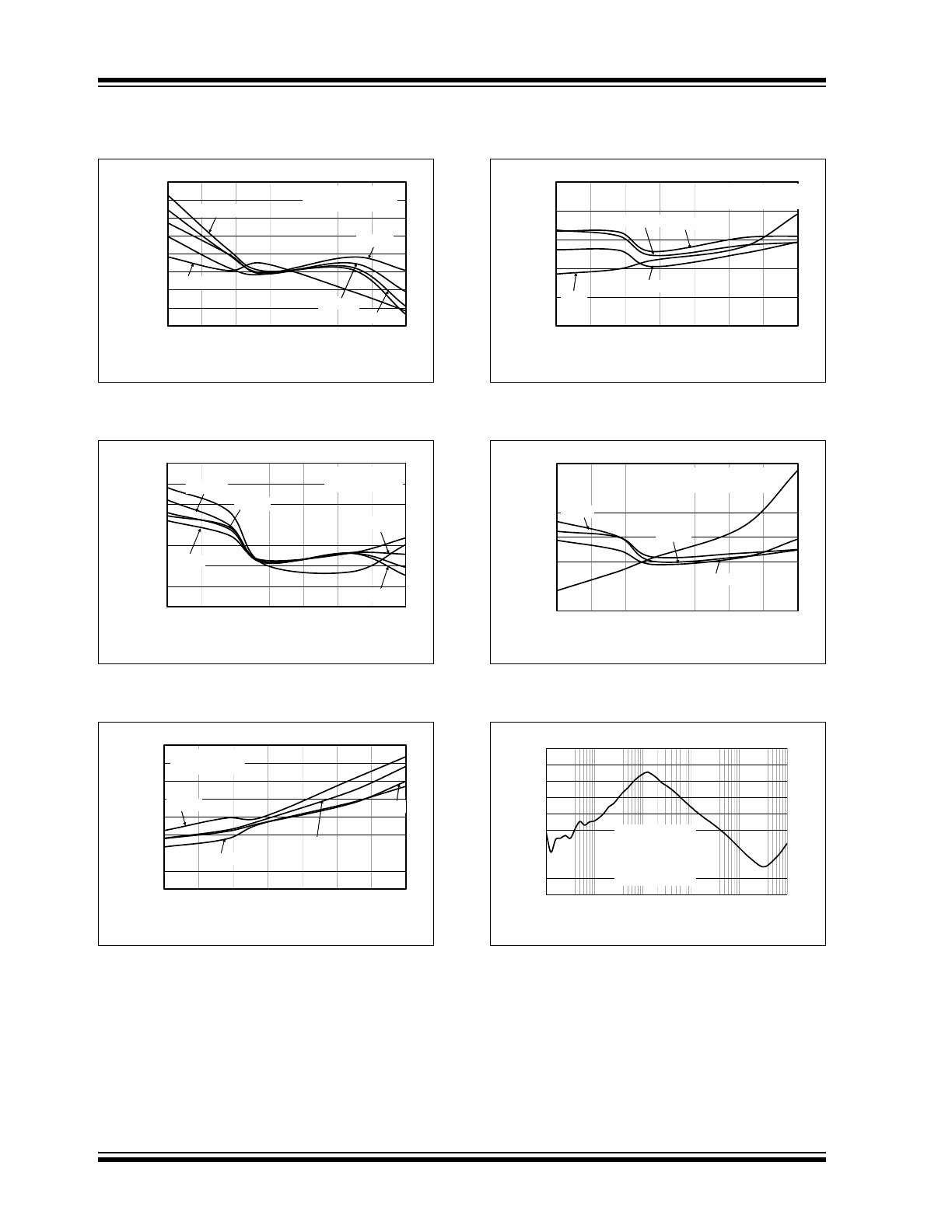
Note: Unless otherwise indicated: V
R
= 1.8V, C
OUT
= 1 µF Ceramic (X7R), C
IN
= 1 µF Ceramic (X7R), I
L
= 100 µA,
T
A
= +25°C, V
IN
= V
OUT(MAX)
+ V
DROPOUT(MAX)
or 2.7V, whichever is greater.
FIGURE 2-19:
Load Regulation vs.
Temperature.
FIGURE 2-20:
Load Regulation vs.
Temperature.
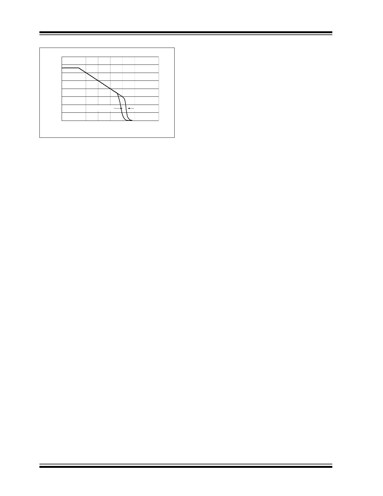
FIGURE 2-21:
Line Regulation vs.
Temperature.
FIGURE 2-22:
Line Regulation vs.
Temperature.
FIGURE 2-23:
Line Regulation vs.
Temperature.
FIGURE 2-24:
PSRR vs. Frequency.
-0.40
-0.20
0.00
0.20
0.40
0.60
0.80
1.00
1.20
-45
-20
5
30
55
80
105
130
Temperature (°C)
Loa
d R
egula
tion
(%
)
V
OUT
= 2.5V
I
OUT
= 1 mA to 250 mA
V
IN
= 3.5V
V
IN
= 14V
V
IN
= 12V
V
IN
= 6V
V
IN
= 16V
-0.40
-0.20
0.00
0.20
0.40
0.60
0.80
1.00
-45
-20
5
30
55
80
105
130
Temperature (°C)
Load
R
e
gul
ati
on (
%
)
V
OUT
= 5.0V
I
OUT
= 1 to 250 mA
V
IN
= 6V
V
IN
= 14V
V
IN
= 12V
V
IN
= 8V
V
IN
= 16V
0.00
0.02
0.04
0.06
0.08
0.10
0.12
0.14
0.16
-45
-20
5
30
55
80
105
130
Temperature (°C)
Li
ne R
egula
tion
(%
/V)
V
IN
= 3.0 to 16.0V
V
OUT
= 1.2V
1 mA
100 mA
0 mA
200 mA
0.00
0.04
0.08
0.12
0.16
0.20
-45
-20
5
30
55
80
105
130
Temperature (°C)
Li
ne R
egula
tion
(%
/V)
V
OUT
= 2.5V
V
IN
= 3.5V to 16V
200 mA
100 mA
0 mA
250 mA
0.06
0.08
0.10
0.12
0.14
0.16
0.18
-45
-20
5
30
55
80
105
130
Temperature (°C)
Li
n
e R
egu
la
ti
on
(%
/V
)
V
OUT
= 5.0V
V
IN
= 6.0V to 16.0V
200mA
100 mA
0 mA
250 mA
-90
-80
-70
-60
-50
-40
-30
-20
-10
0
0.01
0.1
1
10
100
1000
Frequency (kHz)
PSRR (d
B)
V
R
=1.2V
V
IN
=2.7V
V
INAC
= 100 mV p-p
C
IN
=0 μF
I
OUT
=100 µA
© 2011 Microchip Technology Inc.
DS22049F-page 9
MCP1703
Note: Unless otherwise indicated: V
R
= 1.8V, C
OUT
= 1 µF Ceramic (X7R), C
IN
= 1 µF Ceramic (X7R), I
L
= 100 µA,
T
A
= +25°C, V
IN
= V
OUT(MAX)
+ V
DROPOUT(MAX)
or 2.7V, whichever is greater.
FIGURE 2-25:
PSRR vs. Frequency.
FIGURE 2-26:
Output Noise vs. Frequency.
FIGURE 2-27:
Power Up Timing.
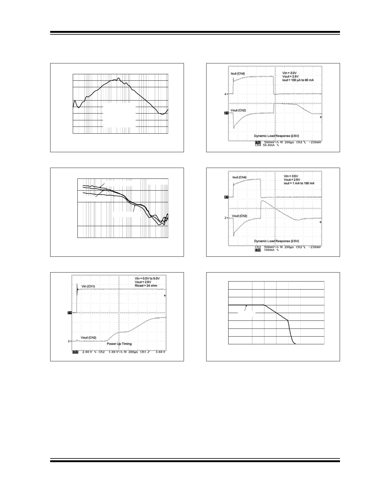
FIGURE 2-28:
Dynamic Load Response.
FIGURE 2-29:
Dynamic Load Response.
FIGURE 2-30:
Output Voltage vs. Input
Voltage.
-90
-80
-70
-60
-50
-40
-30
-20
-10
0
0.01
0.1
1
10
100
1000
Frequency (KHz)
PS
RR
(d
B)
V
R
=5.0V
V
IN
=6.0V
V
INAC
= 100 mV p-p
C
IN
=0 μF
I
OUT
=100 µA
0.001
0.01
0.1
1
10
100
0.01
0.1
1
10
100
1000
Frequency (kHz)
Noi
se (
µ
V
/√
Hz
)
V
R
=5.0V, V
IN
=6.0V
I
OUT
=50 mA
V
R
=2.8V, V
IN
=3.8V
V
R
=1.2V, V
IN
=2.7V
0.0
1.0
2.0
3.0
4.0
0.0
1.0
2.0
3.0
4.0
Input Voltage (V)
O
u
tp
u
t V
o
lt
ag
e
(V
)
R
LOAD
=10 kΩ
V
R
= 2.5V
MCP1703
DS22049F-page 10
© 2011 Microchip Technology Inc.
FIGURE 2-31:
Output Voltage vs. Input
Voltage.
0.0
1.0
2.0
3.0
4.0
0.0
1.0
2.0
3.0
4.0
Input Voltage (V)
O
u
tput V
o
lta
g
e
(V
)
V
R
= 3.3V
I
LOAD
= 1 mA
I
LOAD
= 44 µA