
2018 Microchip Technology Inc.
DS20006054A-page 1
24LC16B
Device Selection Table
Features
• Single Supply with Operation down to 2.5V
• Low-Power CMOS Technology:
- Active current, 1 mA, typical
- Standby current, 1
A, typical
• 2-Wire Serial Interface, I
2
C Compatible
• Schmitt Trigger inputs for Noise Suppression
• Output Slope Control to Eliminate Ground Bounce
• 100 kHz and 400 kHz Clock Compatibility
• Page Write Time 5 ms Maximum
• Self-Timed Erase/Write Cycle
• 16-Byte Page Write Buffer
• Hardware Write-Protect
• ESD Protection > 4,000V
• More than 1 Million Erase/Write Cycles
• Data Retention > 200 Years
• Factory Programming Available
• Packages include 8-lead SOIC and 5-lead SOT-23
• RoHS Compliant
• Temperature Ranges:
- Extended (H): -40°C to +150°C
Description
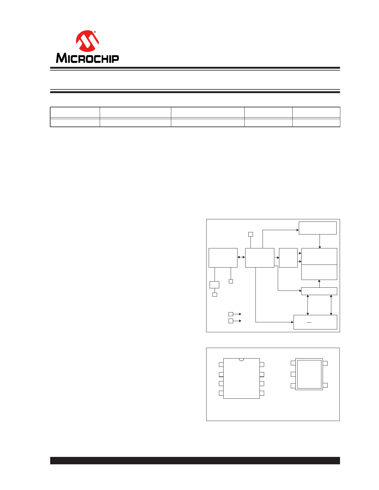
The Microchip Technology Inc. 24LC16B is a 16 Kbit
Electrically Erasable PROM. The device is organized
as eight blocks of 256 x 8-bit memory with a 2-wire
serial interface. Low-voltage design permits operation
down to 2.5V with standby and active currents of only
1
A and 1 mA, respectively. The 24LC16B also has a
page write capability for up to 16 bytes of data. The
24LC16B is available in the standard 8-pin surface
mount SOIC and in the 5-lead SOT-23 packages.
Block Diagram
Package Types (not to scale)
Part Number
V
CC
Range
Max. Clock Frequency
Temp. Ranges
Packages
24LC16B
2.5-5.5V
400 kHz
H
SN, OT
HV
EEPROM
Array
Page
YDEC
XDEC
Sense Amp.
Memory
Control
Logic
I/O
Control
Logic
I/O
WP
SDA
SCL
V
CC
V
SS
R/W Control
Latches
Generator
A0
A1
A2
V
SS
V
CC
WP
SCL
SDA
1
2
3
4
8
7
6
5
SOIC
SOT-23
1
2
3
4
5
WP
V
CC
SCL
V
SS
SDA
Note 1:
Pins A0, A1 and A2 are not used by the 24LC16B
(no internal connections).
16K I
2
C Serial EEPROM High Temp Data Sheet
24LC16B
DS20006054A-page 2
2018 Microchip Technology Inc.
1.0
ELECTRICAL CHARACTERISTICS
Absolute Maximum Ratings
(†)
V
CC
............................................................................................................................................................................ 6.5V
All inputs and outputs w.r.t. V
SS
......................................................................................................... -0.3V to V
CC
+1.0V
Storage Temperature.............................................................................................................................. -65°C to +155°C
Ambient Temperature with Power Applied...........................................................................................-40°C to +150°C
(
1
)
ESD Protection on all Pins
4 kV
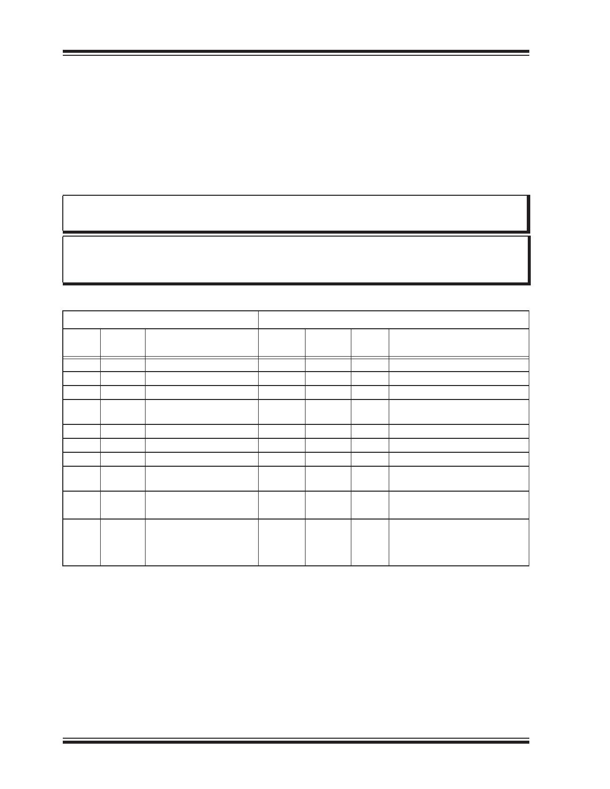
TABLE 1-1:
DC CHARACTERISTICS
Note 1: AEC-Q100 reliability testing for devices intended to operate at 150°C is 1,000 hours. Any design in which
the total operating time from 125°C to 150°C will be greater than 1,000 hours is not warranted without prior
written approval from Microchip Technology Inc.
† NOTICE: Stresses above those listed under “Absolute Maximum Ratings” may cause permanent damage to the
device. This is a stress rating only and functional operation of the device at those or any other conditions above those
indicated in the operational listings of this specification is not implied. Exposure to maximum rating conditions for
extended periods may affect device reliability.
DC CHARACTERISTICS
Extended (H): T
A
= -40°C to +150°C, V
CC
= +2.5V to +5.5V
Param.
No.
Symbol
Characteristic
Min.
Max.
Units
Conditions
WP, SCL and SDA pins
D1
V
IH
High-level input voltage
0.7 V
CC
—
V
—
D2
V
IL
Low-level input voltage
—
0.3
V
CC
V
—
D3
V
HYS
Hysteresis of Schmitt
Trigger inputs
0.05 V
CC
—
V
(
Note 1
)
D4
V
OL
Low-level output voltage
—
0.40
V
I
OL
= 3.0 mA, V
CC
= 2.5V
D5
I
LI
Input leakage current
—
±1
A
V
IN
= V
SS
or V
CC
D6
I
LO
Output leakage current
—
±1
A
V
OUT
= V
SS
or V
CC
D7
C
IN
,
C
OUT
Pin capacitance
(all inputs/outputs)
—
10
pF
V
CC
= 5.0V (
Note 1
)
T
A
= 25°C, F
CLK
= 1 MHz
D8
I
CC
write
Operating current
—
3
mA
V
CC
= 5.5V, SCL = 400 kHz
D9
I
CC
read
—
1
mA
—
D10
I
CCS
Standby current
—
—
1
5
A
A
T
A
= -40°C to +85°C
T
A
= +85°C to +150°C
SDA = SCL = V
CC
WP = V
SS
Note 1: This parameter is periodically sampled and not 100% tested.
2018 Microchip Technology Inc.
DS20006054A-page 3
24LC16B
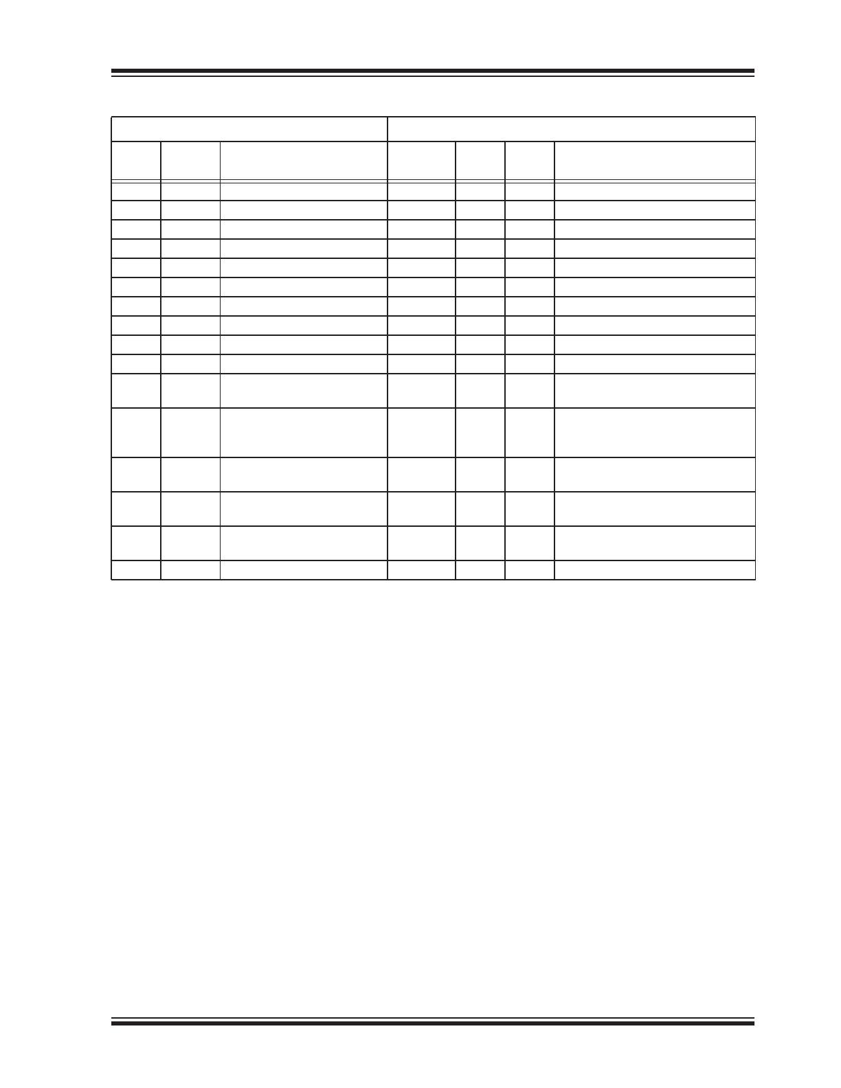
TABLE 1-2:
AC CHARACTERISTICS
AC CHARACTERISTICS
Extended (H): T
A
= -40°C to +150°C, V
CC
= +2.5V to +5.5V
Param.
No.
Symbol
Characteristic
Min.
Max.
Units
Conditions
1
F
CLK
Clock frequency
—
400
kHz
—
2
T
HIGH
Clock High Time
600
—
ns
—
3
T
LOW
Clock Low Time
1300
—
ns
—
4
T
R
SDA and SCL rise time
—
300
ns
(
Note 1
)
5
T
F
SDA and SCL fall time
—
300
ns
(
Note 1
)
6
T
HD
:
STA
Start condition hold time
600
—
ns
—
7
T
SU
:
STA
Start condition setup time
600
—
ns
—
8
T
HD
:
DAT
Data input hold time
0
—
ns
(
Note 2
)
9
T
SU
:
DAT
Data input setup time
100
—
ns
—
10
T
SU
:
STO
Stop condition setup time
600
—
ns
—
11
T
AA
Output valid from clock
(
Note 2
)
—
900
ns
—
12
T
BUF
Bus free time: Time the bus
must be free before a new
transmission can start
1300
—
ns
—
13
T
OF
Output fall time from V
IH
minimum to V
IL
maximum
20+0.1C
B
250
ns
—
14
T
SP
Input filter spike suppression
(SDA and SCL pins)
—
50
ns
(
Notes 1
and
3
)
15
T
WC
Write cycle time
(byte or page)
—
5
ms
—
16
—
Endurance
1M
—
cycles Page mode, 25°C, 5.5V (
Note 4
)
Note 1: Not 100% tested. C
B
= total capacitance of one bus line in pF.
2: As a transmitter, the device must provide an internal minimum delay time to bridge the undefined region
(minimum 300 ns) of the falling edge of SCL to avoid unintended generation of Start or Stop conditions.
3: The combined T
SP
and V
HYS
specifications are due to new Schmitt Trigger inputs which provide improved
noise spike suppression. This eliminates the need for a
T
I
specification for standard operation.
4: This parameter is not tested but ensured by characterization. For endurance estimates in a specific
application, consult the Total Endurance™ Model which can be obtained from Microchip’s website at
www.microchip.com.
24LC16B
DS20006054A-page 4
2018 Microchip Technology Inc.
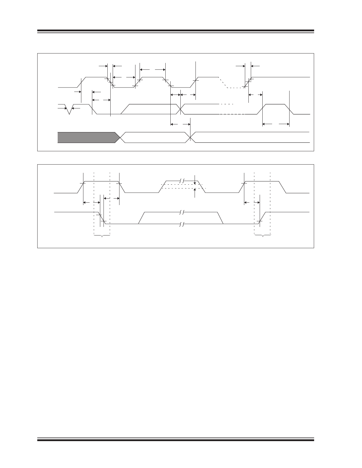
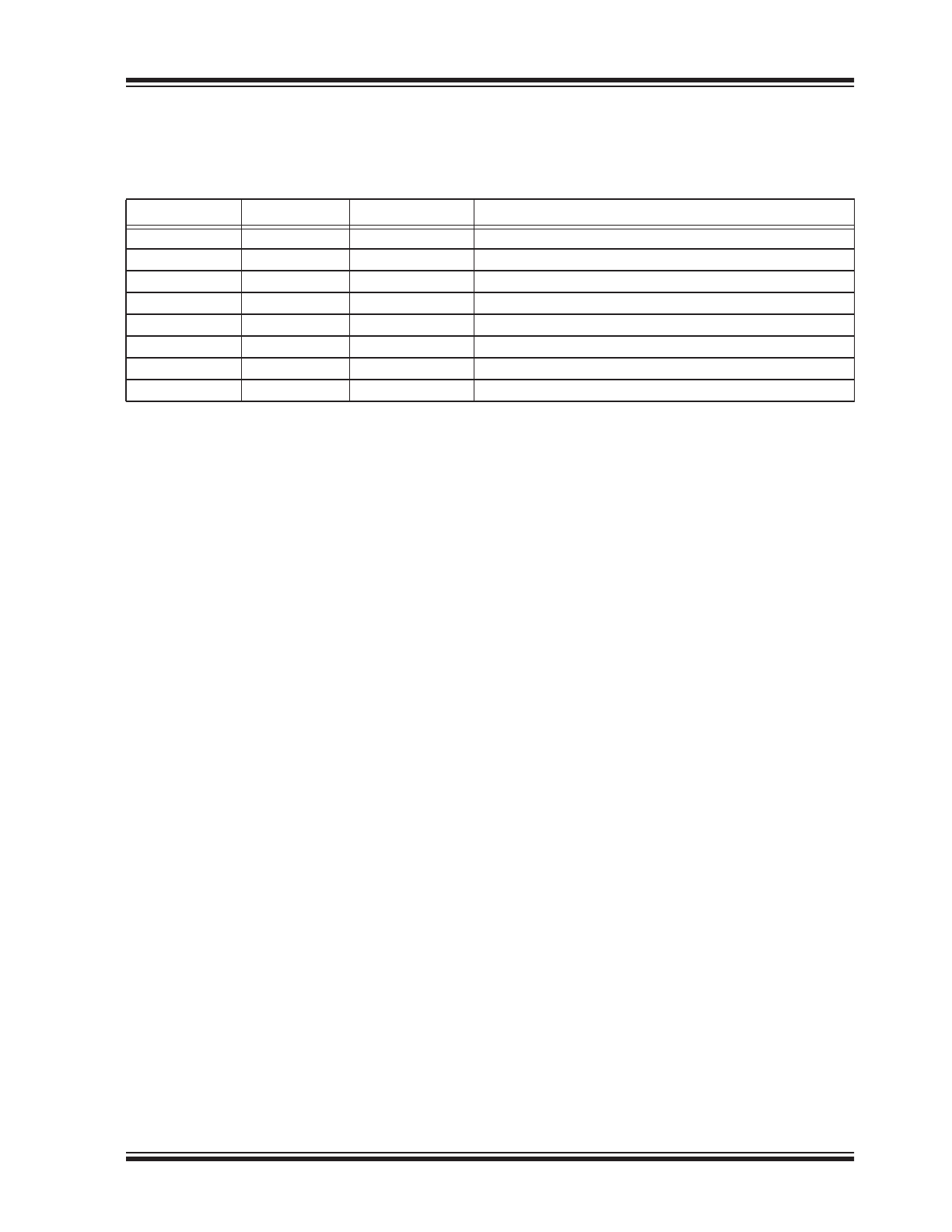
FIGURE 1-1:
BUS TIMING DATA
FIGURE 1-2:
BUS TIMING START/STOP
7
5
2
4
8
9
10
12
11
14
6
SCL
SDA
IN
SDA
OUT
3
7
6
D3
10
Start
Stop
SCL
SDA
2018 Microchip Technology Inc.
DS20006054A-page 5
24LC16B
2.0
PIN DESCRIPTIONS
The descriptions of the pins are listed in
Table 2-1
.
TABLE 2-1:
PIN FUNCTION TABLE
2.1
Serial Address/Data Input/Output
(SDA)
The SDA is a bidirectional pin used to transfer
addresses and data into and out of the device. Since it
is an open-drain terminal, the SDA bus requires a pull-
up resistor to V
CC
(typical 10 k
for 100 kHz, 2 k for
400 kHz).
For normal data transfer, SDA is allowed to change
only during SCL low. Changes during SCL high are
reserved for indicating Start and Stop conditions.
2.2
Serial Clock (SCL)
The SCL input is used to synchronize the data transfer
to and from the device.
2.3
Write-Protect (WP)
The WP pin must be connected to either V
SS
or V
CC
.
If tied to V
SS
, normal memory operation is enabled
(read/write the entire memory 000-7FF).
If tied to V
CC
, write operations are inhibited. The entire
memory will be write-protected. Read operations are
not affected.
2.4
A0, A1, A2
The A0, A1 and A2 pins are not used by the 24LC16B.
They may be left floating or tied to either V
SS
or V
CC
.
Name
SOIC
SOT-23
Description
A0
1
—
Not Connected
A1
2
—
Not Connected
A2
3
—
Not Connected
V
SS
4
2
Ground
SDA
5
3
Serial Address/Data I/O
SCL
6
1
Serial Clock
WP
7
5
Write-Protect Input
V
CC
8
4
+2.5V to 5.5V Power Supply
24LC16B
DS20006054A-page 6
2018 Microchip Technology Inc.
3.0
FUNCTIONAL DESCRIPTION
The 24LC16B supports a bidirectional, 2-wire bus and
data transmission protocol. A device that sends data
onto the bus is defined as a transmitter, while a device
receiving data is defined as a receiver. The bus has to
be controlled by a master device which generates the
Serial Clock (SCL), controls the bus access and
generates the Start and Stop conditions, while the
24LC16B works as slave. Both master and slave can
operate as transmitter or receiver, but the master
device determines which mode is activated.
4.0
BUS CHARACTERISTICS
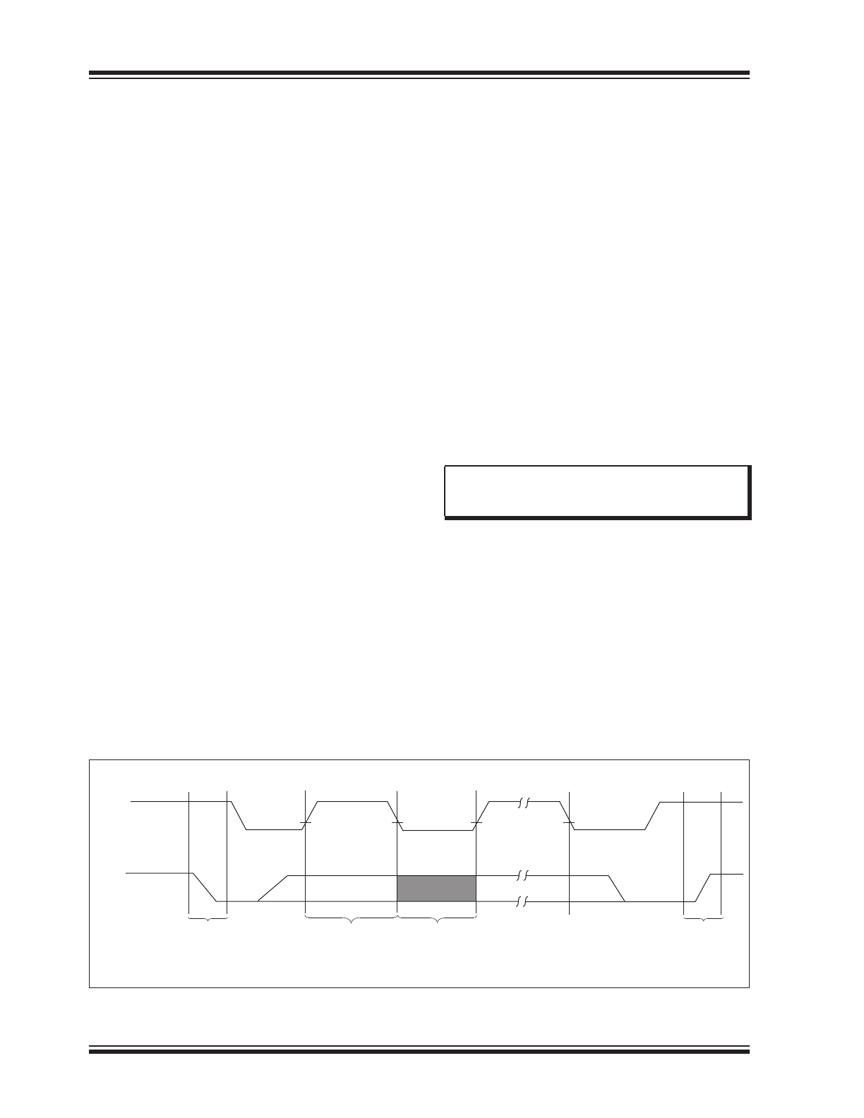
The following bus protocol has been defined:
• Data transfer may be initiated only when the bus
is not busy.
• During data transfer, the data line must remain
stable whenever the clock line is high. Changes in
the data line while the clock line is high will be
interpreted as a Start or Stop condition.
Accordingly, the following bus conditions have been
defined (
Figure 4-1
).
4.1
Bus Not Busy (A)
Both data and clock lines remain high.
4.2
Start Data Transfer (B)
A high-to-low transition of the SDA line while the clock
(SCL) is high determines a Start condition. All
commands must be preceded by a Start condition.
4.3
Stop Data Transfer (C)
A low-to-high transition of the SDA line while the clock
(SCL) is high determines a Stop condition. All
operations must be ended with a Stop condition.
4.4
Data Valid (D)
The state of the data line represents valid data when,
after a Start condition, the data line is stable for the
duration of the high period of the clock signal.
The data on the line must be changed during the low
period of the clock signal. There is one clock pulse per
bit of data.
Each data transfer is initiated with a Start condition and
terminated with a Stop condition. The number of data
bytes transferred between Start and Stop conditions is
determined by the master device and is, theoretically,
unlimited (although only the last sixteen will be stored
when doing a write operation). When an overwrite does
occur it will replace data in a First-in First-out (FIFO)
fashion.
4.5
Acknowledge
Each receiving device, when addressed, is obliged to
generate an Acknowledge after the reception of each
byte. The master device must generate an extra clock
pulse which is associated with this Acknowledge bit.
The device that acknowledges has to pull down the
SDA line during the acknowledge clock pulse in such a
way that the SDA line is stable-low during the high
period of the acknowledge related clock pulse. Setup
and hold times must be taken into account. During
reads, a master must signal an end of data to the slave
by not generating an Acknowledge bit on the last byte
that has been clocked out of the slave. In this case, the
slave (24LC16B) will leave the data line high to enable
the master to generate the Stop condition.
FIGURE 4-1:
DATA TRANSFER SEQUENCE ON THE SERIAL BUS
Note:
The 24LC16B does not generate any
Acknowledge
bits
if
an
internal
programming cycle is in progress.
SCL
SDA
(A)
(B)
(D)
(D)
(A)
(C)
Start
Condition
Address or
Acknowledge
Valid
Data
Allowed
to Change
Stop
Condition
2018 Microchip Technology Inc.
DS20006054A-page 7
24LC16B
5.0
DEVICE ADDRESSING
A control byte is the first byte received following the
Start condition from the master device (
Figure 5-1
).
The control byte consists of a four-bit control code.
For the 24LC16B, this is set as ‘
1010
’ binary for read
and write operations. The next three bits of the control
byte are the block-select bits (B2, B1, B0). They are
used by the master device to select which of the eight
256 word-blocks of memory are to be accessed.
These bits are in effect the three Most Significant bits
(MSb) of the word address. It should be noted that the
protocol limits the size of the memory to eight blocks
of 256 words, therefore, the protocol can support only
one 24LC16B per system.
The last bit of the control byte defines the operation to
be performed. When set to ‘
1
’, a read operation is
selected. When set to ‘
0
’, a write operation is selected.
Following the Start condition, the 24LC16B monitors
the SDA bus, checking the device type identifier being
transmitted and, upon receiving a ‘
1010
’ code, the
slave device outputs an Acknowledge signal on the
SDA line. Depending on the state of the R/W bit, the
24LC16B will select a read or write operation.
FIGURE 5-1:
CONTROL BYTE
ALLOCATION
FIGURE 5-2:
ADDRESS SEQUENCE BIT ASSIGNMENTS
Operation
Control
Code
Block Select
R/W
Read
1010
Block Address
1
Write
1010
Block Address
0
1
0
1
0
B2 B1 B0 R/W ACK
Start bit
Read/Write bit
S
Slave Address
Acknowledge bit
Control Code
Block
Select
bits
1
0
1
0
B
2
B
1
B
0 R/W
A
7
A
0
•
•
•
•
•
•
Control byte
Address Low byte
Control
Code
Block
Select
bits
24LC16B
DS20006054A-page 8
2018 Microchip Technology Inc.
6.0
WRITE OPERATION
6.1
Byte Write
Following the Start condition from the master, the
device code (4 bits), the block address (3 bits) and the
R/W bit, which is a logic-low, is placed onto the bus by
the master transmitter. This indicates to the addressed
slave receiver that a byte with a word address will
follow once it has generated an Acknowledge bit during
the ninth clock cycle. Therefore, the next byte transmit-
ted by the master is the word address and will be
written into the Address Pointer of the 24LC16B. After
receiving another Acknowledge signal from the
24LC16B, the master device will transmit the data word
to be written into the addressed memory location. The
24LC16B acknowledges again and the master
generates a Stop condition. This initiates the internal
write cycle and, during this time, the 24LC16B will not
generate Acknowledge signals (
Figure 6-1
).
6.2
Page Write
The write control byte, word address and the first data
byte are transmitted to the 24LC16B in the same way
as in a byte write. However, instead of generating a
Stop condition, the master transmits up to 16 data
bytes to the 24LC16B, which are temporarily stored in
the on-chip page buffer and will be written into memory
once the master has transmitted a Stop condition.
Upon receipt of each word, the four lower-order
Address Pointer bits are internally incremented by ‘
1
’.
The higher-order 7 bits of the word address remain
constant. If the master should transmit more than 16
bytes prior to generating the Stop condition, the
address counter will roll over and the previously
received data will be overwritten. As with the byte write
operation, once the Stop condition is received an
internal write cycle will begin (
Figure 6-2
).
6.3
Write Protection
The WP pin allows the user to write-protect the entire
array (000-7FF) when the pin is tied to V
CC
. If tied to
V
SS
the write protection is disabled.
FIGURE 6-1:
BYTE WRITE
FIGURE 6-2:
PAGE WRITE
Note:
Page write operations are limited to writ-
ing bytes within a single physical page,
regardless of the number of bytes
actually being written. Physical page
boundaries start at addresses that are
integer multiples of the page buffer size
(or ‘page-size’) and end at addresses that
are integer multiples of [page size – 1]. If
a page write command attempts to write
across a physical page boundary, the
result is that the data wraps around to the
beginning of the current page (overwriting
data previously stored there), instead of
being written to the next page, as might be
expected. It is therefore necessary for the
application software to prevent page write
operations that would attempt to cross a
page boundary.
S
P
Bus Activity
Master
SDA Line
Bus Activity
S
T
A
R
T
S
T
O
P
Control
byte
Word
Address
Data
A
C
K
A
C
K
A
C
K
1 0 1 0 B2 B1 B0 0
Block
Select
bits
S
P
Bus Activity
Master
SDA Line
Bus Activity
S
T
A
R
T
Control
byte
Word
Address
(
n)
Data (n)
Data (n + 15)
S
T
O
P
A
C
K
A
C
K
A
C
K
A
C
K
A
C
K
Data (n + 1)
B1
B2
B0
1 0 1 0
0
Block
Select
bits
2018 Microchip Technology Inc.
DS20006054A-page 9
24LC16B
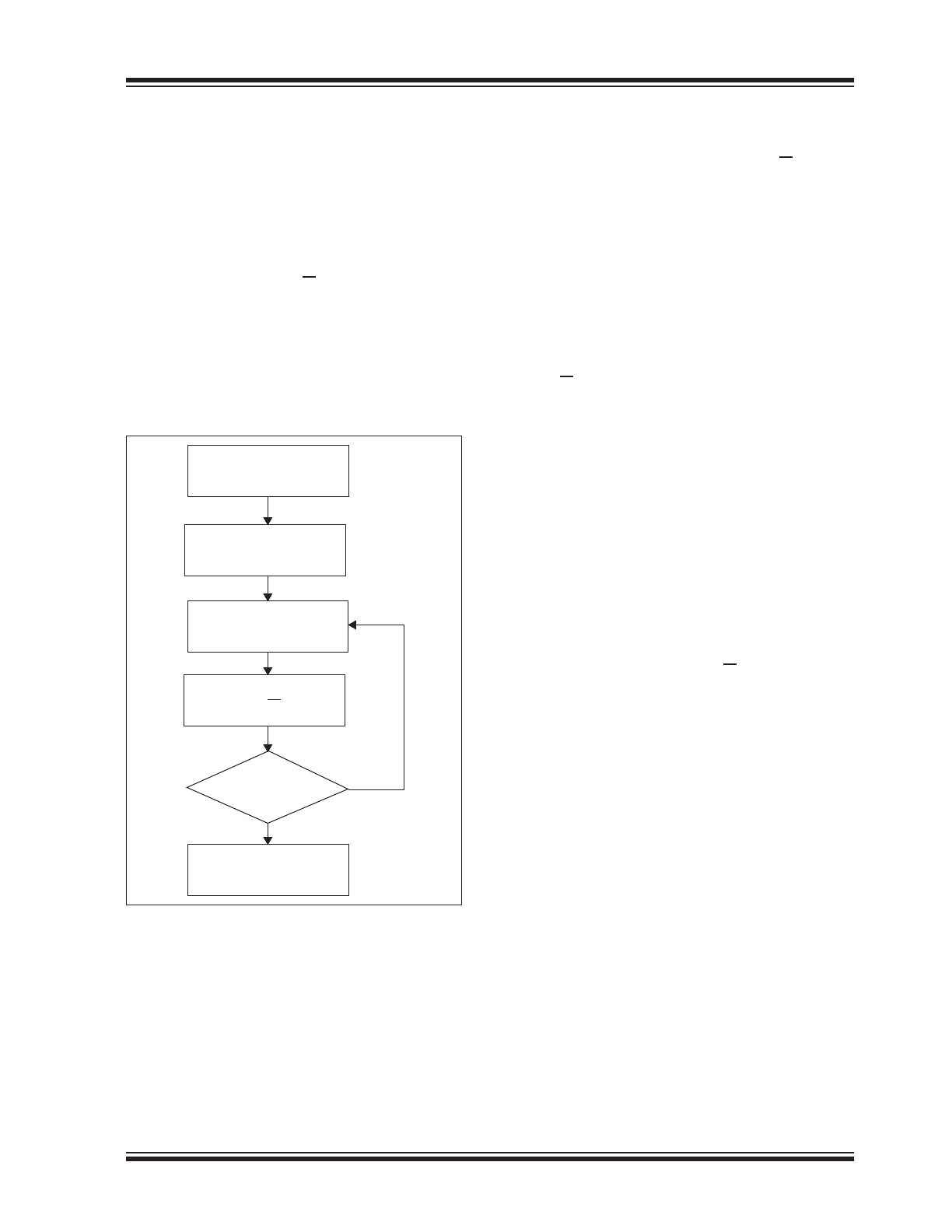
7.0
ACKNOWLEDGE POLLING
Since the device will not acknowledge during a write
cycle, this can be used to determine when the cycle is
complete (this feature can be used to maximize bus
throughput). Once the Stop condition for a write
command has been issued from the master, the device
initiates the internally-timed write cycle and ACK polling
can then be initiated immediately. This involves the
master sending a Start condition followed by the control
byte for a write command (R/W =
0
). If the device is still
busy with the write cycle, no ACK will be returned. If the
cycle is complete, the device will return the ACK and
the master can then proceed with the next read or write
command. See
Figure 7-1
for a flow diagram of this
operation.
FIGURE 7-1:
ACKNOWLEDGE POLLING
FLOW
8.0
READ OPERATION
Read operations are initiated in the same way as write
operations, with the exception that the R/W bit of the
slave address is set to ‘
1
’. There are three basic types
of read operations: current address read, random read
and sequential read.
8.1
Current Address Read
The 24LC16B contains an address counter that main-
tains the address of the last word accessed, internally
incremented by ‘
1
’. Therefore, if the previous access
(either a read or write operation) was to address
n
, the
next current address read operation would access data
from address
n + 1
. Upon receipt of the slave address
with R/W bit set to ‘
1
’, the 24LC16B issues an acknowl-
edge and transmits the 8-bit data word. The master will
not acknowledge the transfer, but does generate a Stop
condition and the 24LC16B discontinues transmission
(
Figure 8-1
).
8.2
Random Read
Random read operations allow the master to access
any memory location in a random manner. To perform
this type of read operation, the word address must first
be set. This is accomplished by sending the word
address to the 24LC16B as part of a write operation.
Once the word address is sent, the master generates a
Start condition following the acknowledge. This
terminates the write operation, but not before the inter-
nal Address Pointer is set. The master then issues the
control byte again, but with the R/W bit set to a ‘
1
’. The
24LC16B will then issue an acknowledge and transmit
the 8-bit data word. The master will not acknowledge
the transfer, but does generate a Stop condition and
the 24LC16B will discontinue transmission (
Figure 8-
2
).
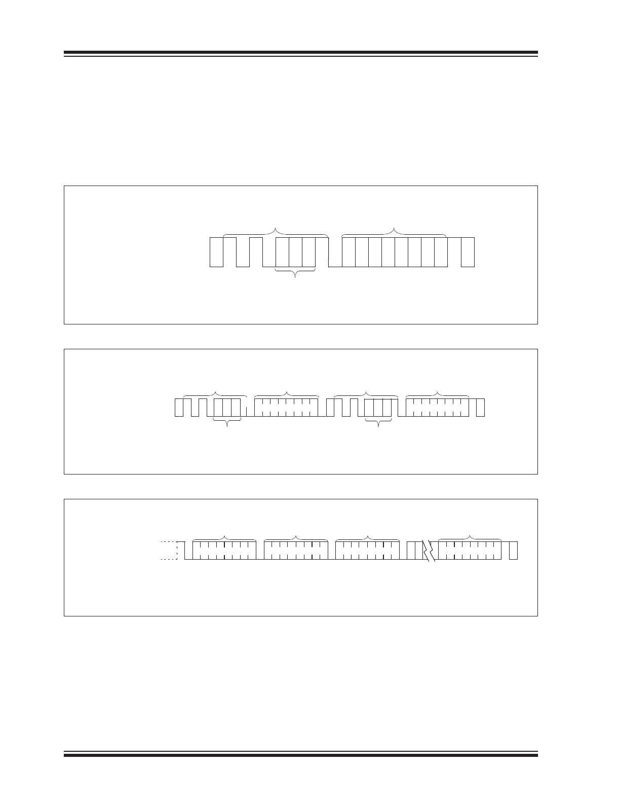
8.3
Sequential Read
Sequential reads are initiated in the same way as a
random read, except that once the 24LC16B transmits
the first data byte, the master issues an acknowledge
as opposed to a Stop condition in a random read. This
directs the 24LC16B to transmit the next sequentially-
addressed 8-bit word (
Figure 8-3
).
To provide sequential reads, the 24LC16B contains an
internal Address Pointer that is incremented by one
upon completion of each operation. This Address
Pointer allows the entire memory contents to be serially
read during one operation.
Send
Write Command
Send Stop
Condition to
Initiate Write Cycle
Send Start
Send Control Byte
with R/W = 0
Did Device
Acknowledge
(ACK = 0)?
Next
Operation
No
Yes
24LC16B
DS20006054A-page 10
2018 Microchip Technology Inc.
8.4
Noise Protection
The 24LC16B employs a V
CC
threshold detector circuit
which disables the internal erase/write logic if the V
CC
is below 1.5V at nominal conditions.
The SCL and SDA inputs have Schmitt Trigger and
filter circuits which suppress noise spikes to assure
proper device operation, even on a noisy bus.
FIGURE 8-1:
CURRENT ADDRESS READ
FIGURE 8-2:
RANDOM READ
FIGURE 8-3:
SEQUENTIAL READ
S
P
Bus Activity
Master
SDA Line
Bus Activity
S
T
O
P
Control
byte
Data (n)
A
C
K
N
o
A
C
K
S
T
A
R
T
1 0 1 0
1
B2 B1 B0
Block
Select
bits
S
P
S
Bus Activity
Master
SDA Line
Bus Activity
S
T
A
R
T
S
T
O
P
Control
byte
A
C
K
Word
Address (n)
Control
byte
S
T
A
R
T
Data (n)
A
C
K
A
C
K
N
o
A
C
K
1 0 1 0
0
B2B1B0
1
1
0
0
1
B2 B1B0
Block
Select
bits
Block
Select
bits
P
Bus Activity
Master
SDA Line
Bus Activity
S
T
O
P
Control
byte
A
C
K
N
o
A
C
K
Data (n)
Data (n + 1)
Data (n + 2)
Data (n + x)
A
C
K
A
C
K
A
C
K
1