
2018 Microchip Technology Inc.
DS20005772B-page 1
24CW16X/24CW32X/24CW64X/24CW128X
Device Selection Table
Features
• 16/32/64/128-Kbit EEPROM:
- Internally organized as one
2048/4096/8192/16384 x 8 bit block
- Byte or page writes up to 32 bytes
- Byte or sequential reads within a block
- Self-timed write cycle (5 ms maximum)
• High-Speed I
2
C Interface:
- Industry standard: 1 MHz, 400 kHz and
100 kHz
- Output slope control to eliminate ground
bounce
- Schmitt trigger inputs for noise suppression
• Programmable Hardware Slave Address Bits:
- Configurable via the Hardware Address
Register (HAR)
• Versatile Data Protection Options:
- Software write protection via the Write
Protection Register (WPR)
• Operating Voltage Range of 1.6V to 5.5V
• Low-Power CMOS Technology:
- Write current: 1.0 mA maximum at 5.5V
- Read current: 1.0 mA maximum at 5.5V,
1 MHz
- Standby Current: 1 µA at 5.5V
• High Reliability:
- More than one million erase/write cycles
- Data retention: >200 years
- ESD protection: >4000V
• RoHS Compliant
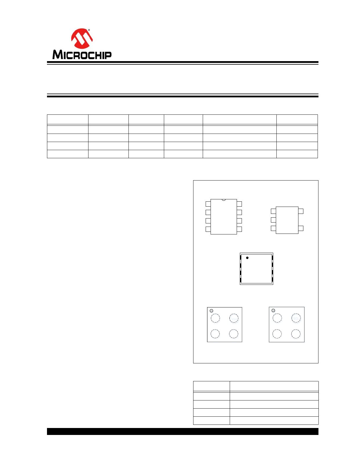
Packages
• 8-Lead SOIC, 8-Lead TSSOP, 8-Pad UDFN,
5-Lead SOT-23 and Two 4-Ball CSP options
Package Types (not to scale)
Pin Function Table
Part Number
Density
Page Size
V
CC
Range
Package
Temp. Ranges
24CW16X
16-Kbit
32-byte
1.6-5.5
SN, OT, ST, MUY
I
24CW32X
32-Kbit
32-byte
1.6-5.5
SN, OT, ST, MUY
I
24CW64X
64-Kbit
32-byte
1.6-5.5
SN, OT, ST, MUY, CS0, CS1
I
24CW128X
128-Kbit
32-byte
1.6-5.5
SN, OT, ST, MUY, CS0, CS1
I
Note:
‘X’ in the part number refers to the preset hardware slave address. Refer to
Table 3-2
for additional information.
Name
Function
V
SS
Ground
SDA
Serial Data Pin
SCL
Serial Clock Input
V
CC
Supply Voltage
8-Pad UDFN
NC
NC
V
SS
NC
SDA
V
CC
8
7
5
1
2
4
NC
3
SCL
6
(Top View)
5-Lead SOT23
(Top View)
8-Lead SOIC/TSSOP
(Top View)
(Top View)
(Top View)
SCL
V
SS
SDA
SDA
V
CC
V
CC
V
CC
V
CC
V
SS
SDA
SCL
SCL
NC
NC
NC
Vss
V
CC
NC
SCL
SDA
1
2
3
4
8
7
6
5
1
2
3
5
4
SCL
V
SS
SDA
NC
V
CC
Note 1:
CS0 CSP ball pitch is 0.4x0.4 mm.
2:
CS1 CSP ball pitch is 0.5x0.4 mm.
4-Ball CSP (CS0)
(
1
)
4-Ball CSP (CS1)
(
2
)
16K-128K I
2
C Serial EEPROM with Software Write
Protection Family Data Sheet
2018 Microchip Technology Inc.
DS20005772B-page 2
24CW16X/24CW32X/24CW64X/24CW128X
Description
The 24CW16X/24CW32X/24CW64X/24CW128X
(24CW Series) devices provide 16-128 Kbits of Serial
EEPROM utilizing an I
2
C (2-wire) serial interface. The
24CW Series is organized as 2048/4096/8192/16384
bytes of 8 bits each (2-16 Kbytes). The 24CW Series is
optimized for use in consumer and industrial applica-
tions, where reliable and dependable nonvolatile mem-
ory storage is essential. The 24CW Series allows up to
eight devices to share a common I
2
C (2-wire) bus and is
capable of operation across a broad voltage range (1.6V
to 5.5V).
The 24CW Series contains a pair of programmable
Configuration registers which allow certain device
behaviors to be modified. These registers are the Write
Protection Register and the Hardware Address
Register.
The Write Protection Register (WPR) controls the valid
address ranges of the EEPROM array that can be writ-
ten. This allows the user to select the write protection
behavior to be configured for software write protection.
The Hardware Address Register (HAR) controls the
three hardware slave address bits. These bits deter-
mine which device addresses the 24CW Series will
Acknowledge. Because the 24CW Series is a 4-pin
device, the cascadable feature is controlled by the
HAR.
Once the desired software write protection and hardware
slave address bits are set, these Configuration registers
can be permanently locked, thereby preventing any
further changes to the device operation.
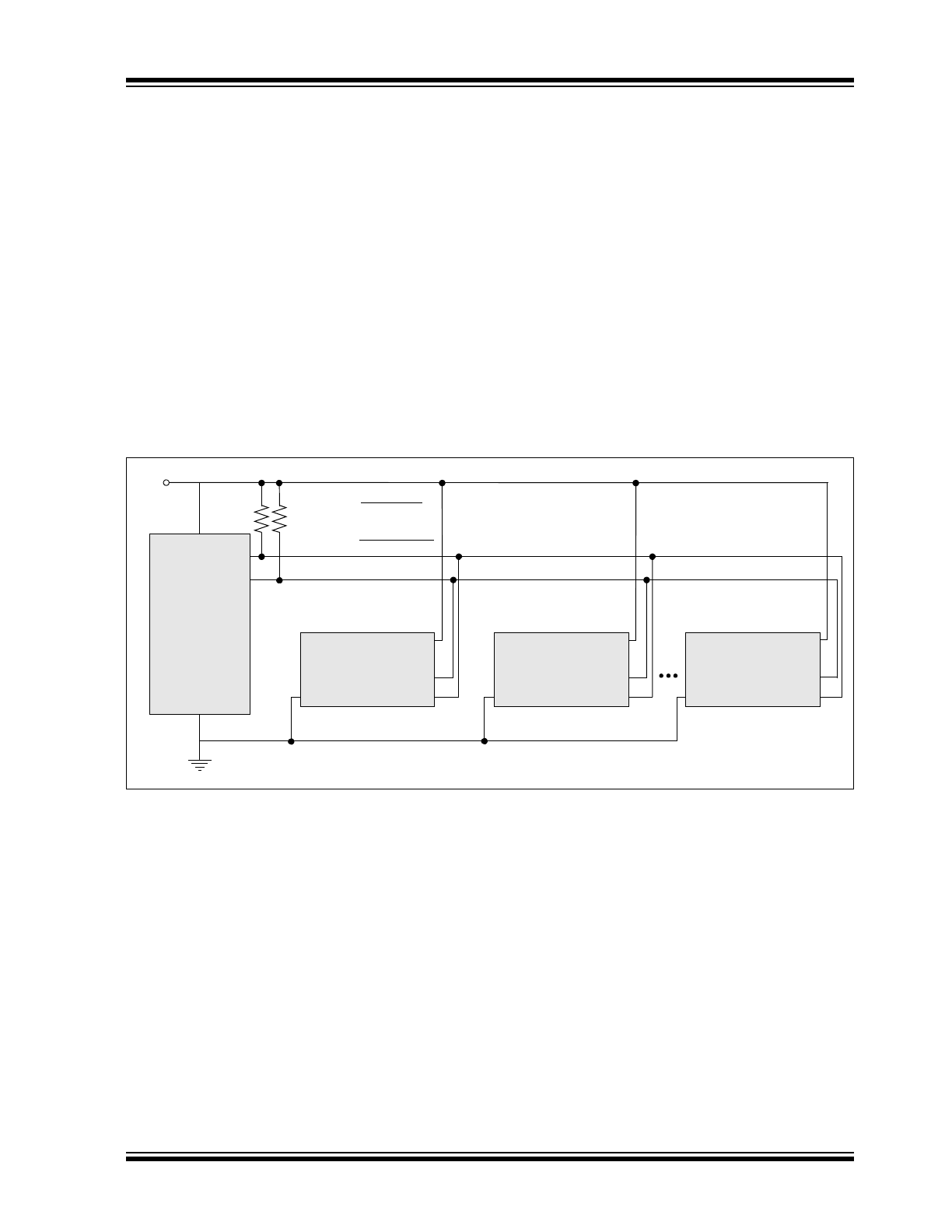
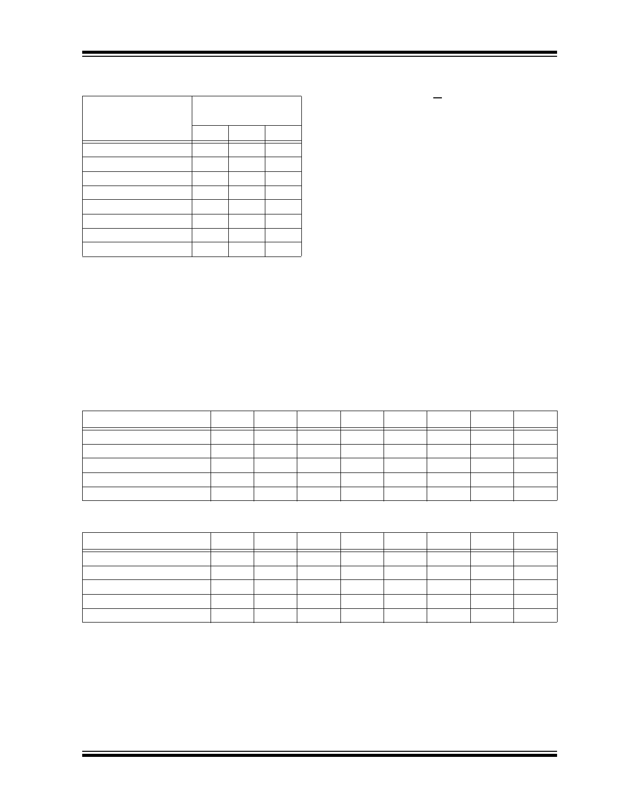
System Configuration Using Serial EEPROMs
I
2
C MCU
V
CC
V
CC
SCL
SDA
V
SS
R
PUP(max)
=
t
R(max)
0.8473
C
L
R
PUP(min)
=
V
CC
– V
OL(max)
I
OL
Programmed
as Slave 0
24CWXXXX
V
CC
SDA
SCL
Programmed
as Slave 1
24CWXXXX
V
CC
SDA
SCL
Programmed
as Slave 7
24CWXXXX
V
CC
SDA
SCL
V
SS
V
SS
V
SS
2018 Microchip Technology Inc.
DS20005772B-page 3
24CW16X/24CW32X/24CW64X/24CW128X
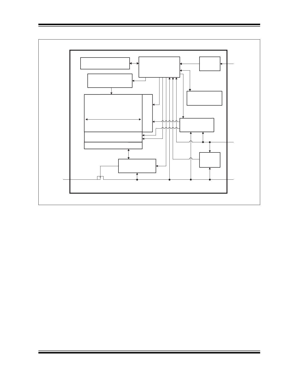
Block Diagram
1 page
Start
Stop
Detector
V
SS
Memory
System Control
Module
High-Voltage
Generation Circuit
Data & ACK
Input/Output Control
Address Register
and Counter
Write Protection
Register
D
OUT
D
IN
V
CC
SCL
SDA
Power-on
Reset
Generator
EEPROM Array
Column Decoder
Row Decoder
Data Register
Hardware Address
Register
2018 Microchip Technology Inc.
DS20005772B-page 4
24CW16X/24CW32X/24CW64X/24CW128X
1.0
ELECTRICAL CHARACTERISTICS
Absolute Maximum Ratings
(†)
V
CC
.............................................................................................................................................................................6.5V
All inputs and outputs w.r.t. V
SS
................................................................................................................... -0.6V to 6.5V
Storage temperature ...............................................................................................................................-65°C to +150°C
Ambient temperature under bias...............................................................................................................-40°C to +85°C
ESD protection on all pins........................................................................................................................................ >4 kV
† NOTICE:
Stresses above those listed under ‘Maximum ratings’ may cause permanent damage to the device. This
is a stress rating only and functional operation of the device at those or any other conditions above those indicated in
the operational listings of this specification is not implied. Exposure to maximum rating conditions for an extended
period of time may affect device reliability.
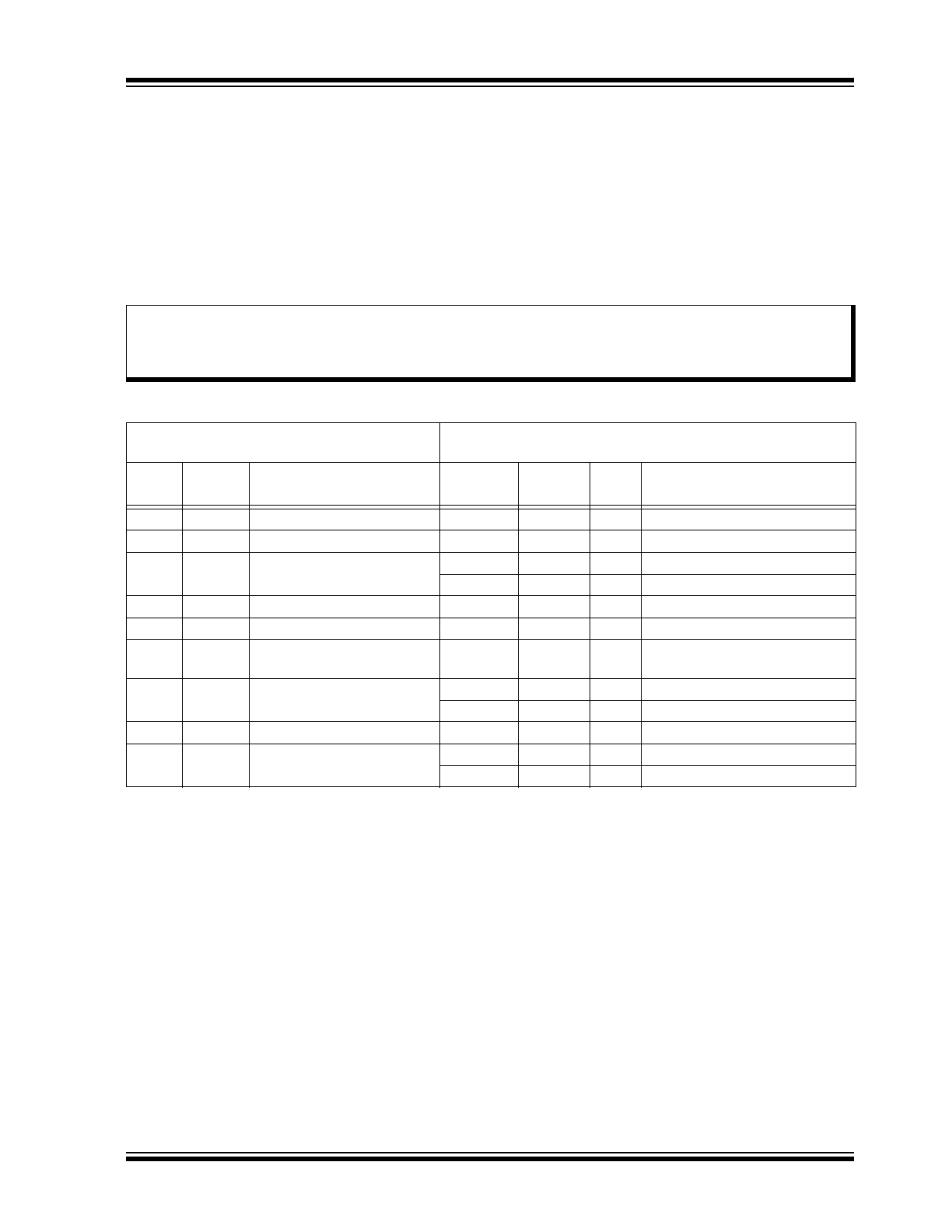
TABLE 1-1:
DC CHARACTERISTICS
DC CHARACTERISTICS
Electrical Characteristics:
Industrial (I):
V
CC
= 1.6V to 5.5V T
A
= -40°C to +85°C
Param.
No.
Symbol
Characteristic
Min.
Max.
Units
Test Conditions
D1
V
IH
High-Level Input Voltage
V
CC X
0.7 V
CC
+ 0.5
V
D2
V
IL
Low-Level Input Voltage
-0.6
V
CC
X
0.3
V
D3
V
OL
Low-Level Output Voltage
—
0.4
V
I
OL
= 2.1 mA, V
CC
= 3.0V
—
0.2
V
I
OL
= 0.15 mA, V
CC
= 1.8V
D4
I
LI
Input Leakage Current
—
±1
µA
V
IN
= V
SS
or V
CC
D5
I
LO
Output Leakage Current
—
±1
µA
V
OUT
= V
SS
or V
CC
D6
C
INT
Internal Capacitance
(all inputs and outputs)
—
7
pF
T
AMB
= +25°C, F
CLK
= 1 MHz,
V
CC
= 5.5V (
Note 1
)
D7
I
CCREAD
Operating Current
—
0.3
mA
V
CC
= 1.8V, F
CLK
= 400 kHz
—
1
mA
V
CC
= 5.5V, F
CLK
= 1 MHz
D8
I
CCWRITE
Operating Current
—
1
mA
V
CC
= 5.5V, F
CLK
= 1 MHz
D9
I
CCS
Standby Current
—
0.5
µA
SCL = SDA = V
CC
= 1.8V
—
1.0
µA
SCL = SDA = V
CC
= 5.5V
Note 1:
This parameter is not tested, but is ensured by characterization.
2018 Microchip Technology Inc.
DS20005772B-page 5
24CW16X/24CW32X/24CW64X/24CW128X
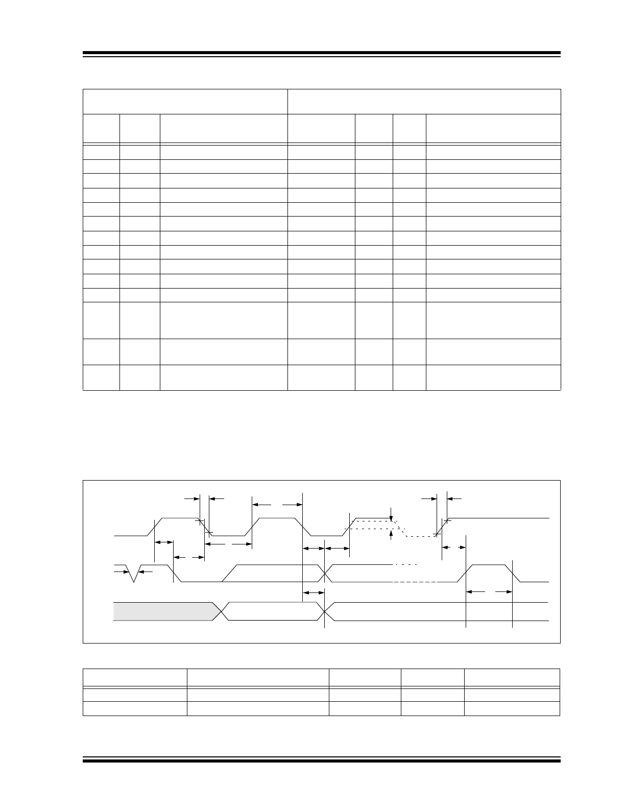
FIGURE 1-1:
BUS TIMING DATA
TABLE 1-3:
EEPROM CELL PERFORMANCE CHARACTERISTICS
TABLE 1-2:
AC CHARACTERISTICS
AC CHARACTERISTICS
Electrical Characteristics:
Industrial (I):
V
CC
= 1.6V to 5.5V T
A
= -40°C to +85°C:
Param.
No.
Symbol
Characteristic
Min.
Max.
Units
Conditions
1
F
CLK
Clock Frequency
—
1000
kHz
1.6V ≤ V
CC
≤ 5.5V
2
T
HIGH
Clock High Time
260
—
ns
1.6V ≤ V
CC
≤ 5.5V
3
T
LOW
Clock Low Time
500
—
ns
1.6V ≤ V
CC
≤ 5.5V
4
T
R
SDA and SCL Rise Time
—
1000
ns
1.6V ≤ V
CC
≤ 5.5V (
Note 1
)
5
T
F
SDA and SCL Fall Time
—
300
ns
1.6V ≤ V
CC
≤ 5.5V (
Note 1
)
6
T
HD
:
STA
Start Condition Hold Time
260
—
ns
1.6V ≤ V
CC
≤ 5.5V
7
T
SU
:
STA
Start Condition Setup Time
260
—
ns
1.6V ≤ V
CC
≤ 5.5V
8
T
HD
:
DAT
Data Input Hold Time
0
—
ns
(
Note 2
)
9
T
SU
:
DAT
Data Input Setup Time
50
—
ns
1.6V ≤ V
CC
≤ 5.5V
10
T
SU
:
STO
Stop Condition Setup Time
260
—
ns
1.6V ≤ V
CC
≤ 5.5V
11
T
AA
Output Valid from Clock
—
450
ns
1.6V ≤ V
CC
≤ 5.5V
12
T
BUF
Bus Free Time: Bus Time
must be Free before a New
Transmission can Start
500
—
ns
1.6V ≤ V
CC
≤ 5.5V
13
T
SP
Input Filter Spike Suppression
(SDA and SCL pins)
—
50
ns
(
Note 3
)
14
T
WC
Write Cycle Time
(byte or page)
—
5
ms
Note 1:
The rise/fall times must be less than the specified maximums in order to achieve the maximum clock
frequencies specified for F
CLK
. Please refer to the I
2
C specification for applicable timings.
2:
As a transmitter, the device must provide an internal minimum delay time to bridge the undefined region of
the falling edge of SCL to avoid unintended generation of Start or Stop conditions.
3:
Not 100% tested. C
B
= total capacitance of one bus line in pF.
Operation
Test Condition
Min.
Max.
Units
Write Endurance
(
1
)
T
A
= 25°C, 1.6V
V
CC
5.5V
1,000,000
—
Write Cycles
Data Retention
(
1
)
T
A
= 55°C
200
—
Years
Note 1:
Performance is determined through characterization and the qualification process.
SCL
SDA
In
SDA
Out
5
7
6
13
3
2
8
9
11
D4
4
10
12
2018 Microchip Technology Inc.
DS20005772B-page 6
24CW16X/24CW32X/24CW64X/24CW128X
1.1
Power-up Requirements and
Reset Behavior
During a power-up sequence, the V
CC
supplied to the
24CW Series should monotonically rise from V
SS
to the
minimum V
CC
level, as specified in
Table 1-1
, with a
slew rate no faster than 0.1V/µs.
1.1.1
DEVICE RESET
To prevent write operations or other spurious events
from happening during a power-up sequence, the
24CW Series includes a Power-on Reset (POR) circuit.
Upon power-up, the device will not respond to any
commands until the V
CC
level crosses the internal volt-
age threshold (V
POR
) that brings the device out of
Reset and into Standby mode.
The system designer must ensure that instructions are
not sent to the device until the V
CC
supply has reached
a stable value greater than, or equal to, the minimum
V
CC
level. Additionally, once the V
CC
is greater than, or
equal to, the minimum V
CC
level, the master must wait
at least T
PUP
before sending the first command to the
device. See
Table 1-4
for the values associated with
these power-up parameters.
If an event occurs in the system where the V
CC
level
supplied to the 24CW Series drops below the maxi-
mum V
POR
level specified, it is recommended that a
full-power cycle sequence be performed by first driving
the V
CC
pin to V
SS
, waiting at least the minimum T
POFF
time and then perform a new power-up sequence
in compliance with the requirements defined in
Section 1.1 “Power-up Requirements and Reset
Behavior”
.
TABLE 1-4:
POWER-UP CONDITIONS
Symbol
Parameter
Min.
Max.
Units
T
PUP
Time Required after V
CC
is Stable before the Device can Accept Commands
100
—
µs
V
POR
Power-on Reset Threshold Voltage
—
1.5
V
T
POFF
Minimum Time at V
CC
= 0V between Power Cycles
1
—
ms
2018 Microchip Technology Inc.
DS20005772B-page 7
24CW16X/24CW32X/24CW64X/24CW128X
2.0
PIN DESCRIPTIONS
The descriptions of the pins are listed in
Table 2-1
.
2.1
Serial Data (SDA)
This is a bidirectional pin used to transfer addresses
and data into and out of the device. It is an open-drain
terminal, therefore, the SDA bus requires a pull-up
resistor to V
CC
(typical 10 kΩ for 100 kHz and 2 kΩ for
400 kHz and 1 MHz).
For normal data transfer, SDA is allowed to change
only during SCL low. Changes during SCL high are
reserved for indicating the Start and Stop conditions.
2.2
Serial Clock (SCL)
This input is used to synchronize the data transfer from
and to the device.
TABLE 2-1:
PIN FUNCTION TABLE
Name
8-Lead
SOIC
8-Lead
TSSOP
5-Lead
SOT23
8-Lead
UDFN
(
1
)
4-Ball CSP
(CS0)
(
2
)
4-Ball CSP
(CS1)
(
3
)
Function
NC
1
1
—
1
—
—
No Connect
NC
2
2
—
2
—
—
No Connect
NC
3
3
—
3
—
—
No Connect
V
SS
4
4
2
4
A2
B2
Ground
SDA
5
5
3
5
B2
B1
Serial Data
SCL
6
6
1
6
B1
A2
Serial Clock
NC
7
7
5
7
—
—
No Connect
V
CC
8
8
4
8
A1
A1
Device Power Supply
Note 1:
The exposed pad on this package can be connected to V
SS
or left floating.
2:
CS0 CSP ball pitch is 0.4x0.4 mm.
3:
CS1 CSP ball pitch is 0.5x0.4 mm.
2018 Microchip Technology Inc.
DS20005772B-page 8
24CW16X/24CW32X/24CW64X/24CW128X
3.0
MEMORY ORGANIZATION
3.1
EEPROM Organization
The 24CW Series is internally organized as
64/128/256/512 pages of 32 bytes each, depending on
the density.
3.2
Device Configuration Registers
The 24CW Series contains two Configuration registers
that modulate device operation and/or report on the
current status of the device. These registers are:
• Write Protection Register (WPR)
• Hardware Address Register (HAR)
Once the device behavior is set as desired, the Config-
uration registers can be permanently locked (or set to
read-only), thereby preventing any subsequent
changes.
3.2.1
WRITE PROTECTION REGISTER
The Write Protection Register (WPR) allows for modifi-
cation of the device write protection behavior. Refer to
Section 8.2 “Write Protection Register”
for additional
information of the WPR.
3.2.2
HARDWARE ADDRESS REGISTER
The Hardware Address Register (HAR) allows for
modification of the hardware slave address bits in the
device address byte that the device will Acknowledge.
Refer to
Section 8.3 “Hardware Address Register”
for additional information on the HAR.
3.3
Device Addressing
Communication with the 24CW Series begins with an
8-bit device address byte, comprised of a 7-bit slave
address and a Read/Write Select (R/W) bit. Since
multiple slave devices can reside on the serial bus,
each slave device must have its own unique device
address, programmed in the HAR, so that the master
can access each device independently.
The 7-bit slave address is constructed using two
groups of bits. The first four bits contain the Device
Type Identifier, followed by three bits containing the
hardware slave address bits.
The 24CW Series will respond to only specific Device
Type Identifiers, as shown in
Section 3.3.1 “Valid
Device Address Byte Inputs”
.
The 3-bit hardware slave address is comprised of
bits A2, A1 and A0. These bits can be used to expand
the address space by allowing up to eight devices with
the same Device Type Identifiers on the bus. These
hardware slave address bits must correlate with the
values programmed in the HAR.
The device will respond to all valid device address byte
combinations that it receives.
3.3.1
VALID DEVICE ADDRESS BYTE
INPUTS
The 24CW Series will respond to the Device Type
Identifiers, as shown in
Table 3-1
.
3.3.1.1
Preset Slave Addresses
The 24CW Series is preset with a specific slave
address. The preset slave address bits are embedded
in the base part number, as shown in
Table 3-2
.
TABLE 3-1:
TABLE OF VALID DEVICE ADDRESS BYTES
Access Region
Device Type Identifier
Hardware Slave Address
Read/Write
Select
Bit 7
Bit 6
Bit 5
Bit 4
Bit 3
Bit 2
Bit 1
Bit 0
EEPROM
1
0
1
0
A2
A1
A0
R/W
Configuration Registers
1
0
1
0
A2
A1
A0
R/W
Note:
The access region is selected according to bit 7 of the first word address byte. Refer to
Section 3.3.2
“Word Address Bytes”
for additional information.
2018 Microchip Technology Inc.
DS20005772B-page 9
24CW16X/24CW32X/24CW64X/24CW128X
TABLE 3-2:
DEVICE PRESET SLAVE
ADDRESS
3.3.1.2
Read/Write Select Bit
The eighth bit (bit 0) of the device address byte is the
Read/Write Select (R/W) bit. A read operation is
initiated if this bit is a logic ‘1’ and a write operation is
initiated if this bit is a logic ‘0’.
Upon the successful comparison of the device address
byte, the 24CW Series will respond. If a valid compari-
son is not made, the device will not respond and return
to a standby state.
3.3.2
WORD ADDRESS BYTES
Two 8-bit word address bytes are transmitted to the
device immediately following the device address byte.
The first word address byte contains the Most Signifi-
cant bits (MSbs) of the memory array word address to
specify which location in the EEPROM to start reading
or writing. Note that the number of word address bits
depends on the density. Refer to
Table 3-3
for details.
When accessing the memory array, it is required that
bit 7 of the word address byte be set to a logic ‘0’.
When accessing the Configuration registers, it is
required that bit 7 of the first word address byte be set
to a logic ‘1’. Refer to
Table 3-3
for details.
Next, the second word address byte is sent to the device
which provides the remaining eight bits of the word
address (A7 through A0). Refer to
Table 3-4
for details.
TABLE 3-3:
FIRST WORD ADDRESS BYTE
TABLE 3-4:
SECOND WORD ADDRESS BYTE
Part Number Series
24CWXXXX
Hardware Slave
Address Bits
A2
A1
A0
24CWXXX0
(
1
)
0
0
0
24CWXXX1
(
1
,
2
)
0
0
1
24CWXXX2
(
1
,
2
)
0
1
0
24CWXXX3
(
1
,
2
)
0
1
1
24CWXXX4
(
1
,
2
)
1
0
0
24CWXXX5
(
1
,
2
)
1
0
1
24CWXXX6
(
1
,
2
)
1
1
0
24CWXXX7
(
1
,
2
)
1
1
1
Note 1:
‘XXX’ in the part number varies depending
on the density.
2:
Contact your local sales representative for
hardware slave address availability.
Memory Region
Bit 7
Bit 6
Bit 5
Bit 4
Bit 3
Bit 2
Bit 1
Bit 0
16-Kbit EEPROM
0
x
x
x
x
A10
A9
A8
32-Kbit EEPROM
0
x
x
x
A11
A10
A9
A8
64-Kbit EEPROM
0
x
x
A12
A11
A10
A9
A8
128-Kbit EEPROM
0
x
A13
A12
A11
A10
A9
A8
Configuration Registers
1
x
x
x
x
x
x
x
Memory Region
Bit 7
Bit 6
Bit 5
Bit 4
Bit 3
Bit 2
Bit 1
Bit 0
16-Kbit EEPROM
A7
A6
A5
A4
A3
A2
A1
A0
32-Kbit EEPROM
A7
A6
A5
A4
A3
A2
A1
A0
64-Kbit EEPROM
A7
A6
A5
A4
A3
A2
A1
A0
128-Kbit EEPROM
A7
A6
A5
A4
A3
A2
A1
A0
Configuration Registers
(
1
)
x
x
x
x
x
x
x
x
Note 1:
When accessing the Configuration registers, the second word address byte must be transmitted to the
device despite containing only don’t care values.
2018 Microchip Technology Inc.
DS20005772B-page 10
24CW16X/24CW32X/24CW64X/24CW128X
4.0
FUNCTIONAL DESCRIPTION
The 24CW Series supports a bidirectional 2-wire bus
and data transmission protocol. A device that sends
data onto the bus is defined as a transmitter and a
device receiving data as a receiver. The bus must be
controlled by a master which generates the Serial
Clock (SCL), controls the bus access and generates
the Start and Stop conditions, while the 24CW Series
works as a slave. Both master and slave can operate
as a transmitter or receiver, but the master determines
which mode is activated.
5.0
BUS CHARACTERISTICS
The following bus protocol has been defined:
• Data transfer may be initiated only when the bus
is not busy.
• During data transfer, the data line must remain
stable whenever the clock line is high. Changes in
the data line, while the clock line is high, will be
interpreted as a Start or Stop condition.
Accordingly, the following bus conditions have been
defined (
Figure 5-1
).
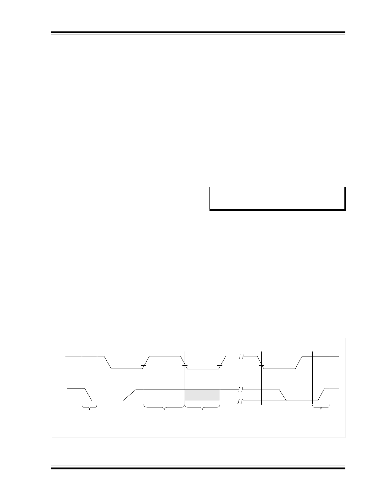
5.1
Bus Not Busy (A)
Both data and clock lines remain high.
5.2
Start Data Transfer (B)
A high-to-low transition of the SDA line while the clock
(SCL) is high determines a Start condition. All
commands must be preceded by a Start condition.
5.3
Stop Data Transfer (C)
A low-to-high transition of the SDA line while the clock
(SCL) is high determines a Stop condition. All
operations must end with a Stop condition.
5.4
Data Valid (D)
The state of the data line represents valid data when,
after a Start condition, the data line is stable for the
duration of the high period of the clock signal.
The data on the line must be changed during the low
period of the clock signal. There is one bit of data per
clock pulse.
Each data transfer is initiated with a Start condition and
terminated with a Stop condition. The number of the
data bytes transferred between the Start and Stop
conditions is determined by the master.
5.5
Acknowledge
Each receiving device, when addressed, is obliged to
generate an Acknowledge signal after the reception of
each byte. The master must generate an extra clock
pulse, which is associated with this Acknowledge bit.
See
Figure 5-2
for Acknowledge timing.
A device that Acknowledges must pull down the SDA
line during the Acknowledge clock pulse, in such a way,
that the SDA line is stable low during the high period of
the Acknowledge related clock pulse. Of course, setup
and hold times must be taken into account. During read
operations, the master must signal an end of data to the
slave by NOT generating an Acknowledge (NACK) bit
on the last byte that has been clocked out of the slave.
In this case, the slave (24CW Series) will leave the data
line high to enable the master to generate the Stop
condition.
FIGURE 5-1:
DATA TRANSFER SEQUENCE ON THE SERIAL BUS
Note:
The 24CW Series does not generate
any Acknowledge bits if an internal
programming cycle is in progress.
Address or
Acknowledge
Valid
Data
Allowed
to Change
Stop
Condition
Start
Condition
SCL
SDA
(A)
(B)
(D)
(D)
(C)
(A)