
2012 Microchip Technology Inc.
Preliminary
DS25157A-page 1
23LCV512
Device Selection Table
Features:
• SPI-Compatible Bus Interface:
- 20 MHz Clock rate
- SPI/SDI mode
• Low-Power CMOS Technology:
- Read Current: 3 mA at 5.5V, 20 MHz
- Standby Current: 4
A at +85°C
• Unlimited Read and Write Cycles
• External Battery Backup support
• Zero Write Time
• 64K x 8-bit Organization:
- 32-byte page
• Byte, Page and Sequential mode for Reads and
Writes
• High Reliability
• Temperature Range Supported:
• Pb-Free and RoHS Compliant, Halogen Free.
• 8-Lead SOIC, TSSOP and PDIP Packages
Pin Function Table
Description:
The Microchip Technology Inc. 23LCV512 is a 512 Kbit
Serial SRAM device. The memory is accessed via a
simple Serial Peripheral Interface (SPI) compatible
serial bus. The bus signals required are a clock input
(SCK) plus separate data in (SI) and data out (SO)
lines. Access to the device is controlled through a Chip
Select (CS) input. Additionally, SDI (Serial Dual Inter-
face) is supported if your application needs faster data
rates.
This device also supports unlimited reads and writes to
the memory array, and supports data backup via exter-
nal battery/coin cell connected to V
BAT
(pin 7).
The 23LCV512 is available in standard packages
including 8-lead SOIC, PDIP and advanced 8-lead
TSSOP.
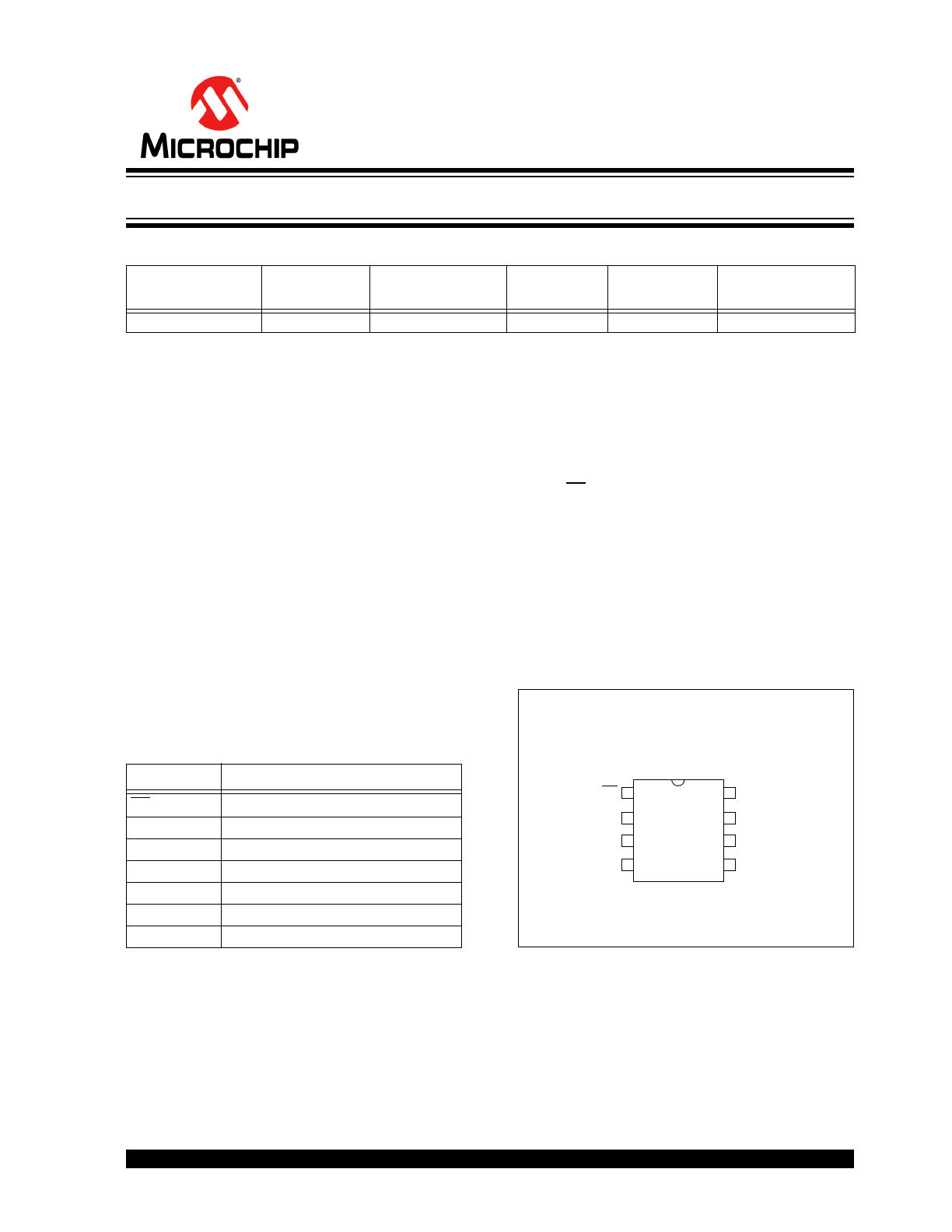
Package Types (not to scale)
Part
Number
V
CC
Range
Dual I/O
(SDI)
Battery
Backup
Max. Clock
Frequency
Packages
23LCV512
2.5-5.5V
Yes
Yes
20 MHz
SN, ST, P
- Industrial (I):
-40
C to +85C
Name
Function
CS
Chip Select Input
SO/SIO1
Serial Output/SDI pin
Vss
Ground
SI/SIO0
Serial Input/SDI pin
SCK
Serial Clock
V
BAT
External Backup Supply Input
Vcc
Power Supply
CS
SO/SIO1
NC
Vss
Vcc
V
BAT
SCK
SI/SIO0
1
2
3
4
8
7
6
5
SOIC/TSSOP/PDIP
512 Kbit SPI Serial SRAM with Battery Backup and SDI Interface
23LCV512
DS25157A-page 2
Preliminary
2012 Microchip Technology Inc.
1.0
ELECTRICAL CHARACTERISTICS
Absolute Maximum Ratings
(†)
V
CC
.............................................................................................................................................................................6.5V
All inputs and outputs w.r.t. V
SS
......................................................................................................... -0.3V to V
CC
+0.3V
Storage temperature ...............................................................................................................................-65°C to +150°C
Ambient temperature under bias ...............................................................................................................-40°C to +85°C
TABLE 1-1:
DC CHARACTERISTICS
† NOTICE: Stresses above those listed under “Absolute Maximum Ratings” may cause permanent damage to the
device. This is a stress rating only and functional operation of the device at those or any other conditions above those
indicated in the operational listings of this specification is not implied. Exposure to maximum rating conditions for an
extended period of time may affect device reliability.
DC CHARACTERISTICS
Industrial (I):
T
A
= -40°C to +85°C
Param.
No.
Sym.
Characteristic
Min.
Typ.
(1)
Max.
Units
Test Conditions
D001
V
CC
Supply voltage
2.5
—
5.5
V
23LCV512
D002
V
IH
High-level input
voltage
.7 V
CC
—
V
CC
+0.3
V
D003
V
IL
Low-level input
voltage
-0.3
—
0.10xV
CC
V
23LCV512
D004
V
OL
Low-level output
voltage
—
—
0.2
V
I
OL
= 1 mA
D005
V
OH
High-level output
voltage
V
CC
-0.5
—
—
V
I
OH
= -400
A
D006
I
LI
Input leakage
current
—
—
±1
A
CS = V
CC
, V
IN
= V
SS
OR
V
CC
D007
I
LO
Output leakage
current
—
—
±1
A
CS = V
CC
, V
OUT
= V
SS
OR
V
CC
D008
I
CC
Read Operating current
—
3
10
mA
F
CLK
= 20 MHz; SO = O, 5.5V
D009
I
CCS
Standby current
—
4
10
A
CS = V
CC
= 5.5V, Inputs tied to
V
CC
or V
SS
D010
C
INT
Input capacitance
—
—
7
pF
V
CC
= 0V, f = 1 MHz, Ta = 25°C
(
Note 1
)
D011
V
DR
RAM data retention
voltage
—
1.0
—
V
(
Note 2
)
D012
V
TRIP
V
BAT
Change Over
1.6
1.8
2.0
V
Typical at Ta = 25°C
(
Note 1
)
D013
V
BAT
V
BAT
Voltage Range
1.4
—
3.6
V
(
Note 1
)
D014
IBAT
V
BAT
Current
—
1
—
A
Typical at 2.5V, Ta = 25°C
(
Note 1
)
Note 1:
This parameter is periodically sampled and not 100% tested. Typical measurements taken at room
temperature (25°C).
2:
This is the limit to which V
DD
can be lowered without losing RAM data. This parameter is periodically
sampled and not 100% tested.
2012 Microchip Technology Inc.
Preliminary
DS25157A-page 3
23LCV512
TABLE 1-3:
AC TEST CONDITIONS
TABLE 1-2:
AC CHARACTERISTICS
AC CHARACTERISTICS
Industrial (I):
T
A
= -40°C to +85°C
Param.
No.
Sym.
Characteristic
Min.
Max.
Units
Test Conditions
1
F
CLK
Clock frequency
—
20
MHz
2
T
CSS
CS setup time
25
—
ns
3
T
CSH
CS hold time
50
—
ns
4
T
CSD
CS disable time
25
—
ns
5
Tsu
Data setup time
10
—
ns
6
T
HD
Data hold time
10
—
ns
7
T
R
CLK rise time
—
20
ns
Note 1
8
T
F
CLK fall time
—
20
ns
Note 1
9
T
HI
Clock high time
25
—
ns
10
T
LO
Clock low time
25
—
ns
11
T
CLD
Clock delay time
25
—
ns
12
T
V
Output valid from clock low
—
25
ns
13
T
HO
Output hold time
0
—
ns
Note 1
14
T
DIS
Output disable time
—
20
ns
Note 1:
This parameter is periodically sampled and not 100% tested.
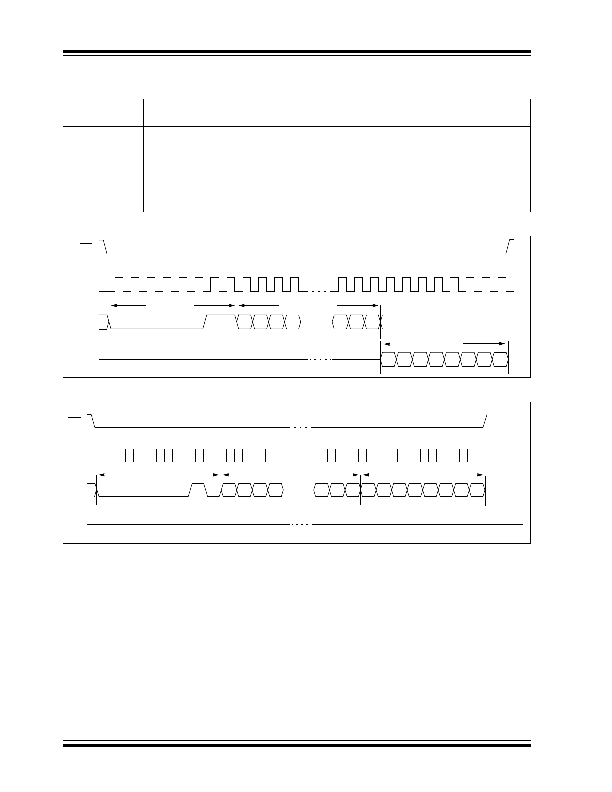
AC Waveform:
Input pulse level
0.1 V
CC
to 0.9 V
CC
Input rise/fall time
5 ns
Operating temperature
-40°C to +85°C
C
L
= 30 pF
—
Timing Measurement Reference Level:
Input
0.5 V
CC
Output
0.5 V
CC
23LCV512
DS25157A-page 4
Preliminary
2012 Microchip Technology Inc.
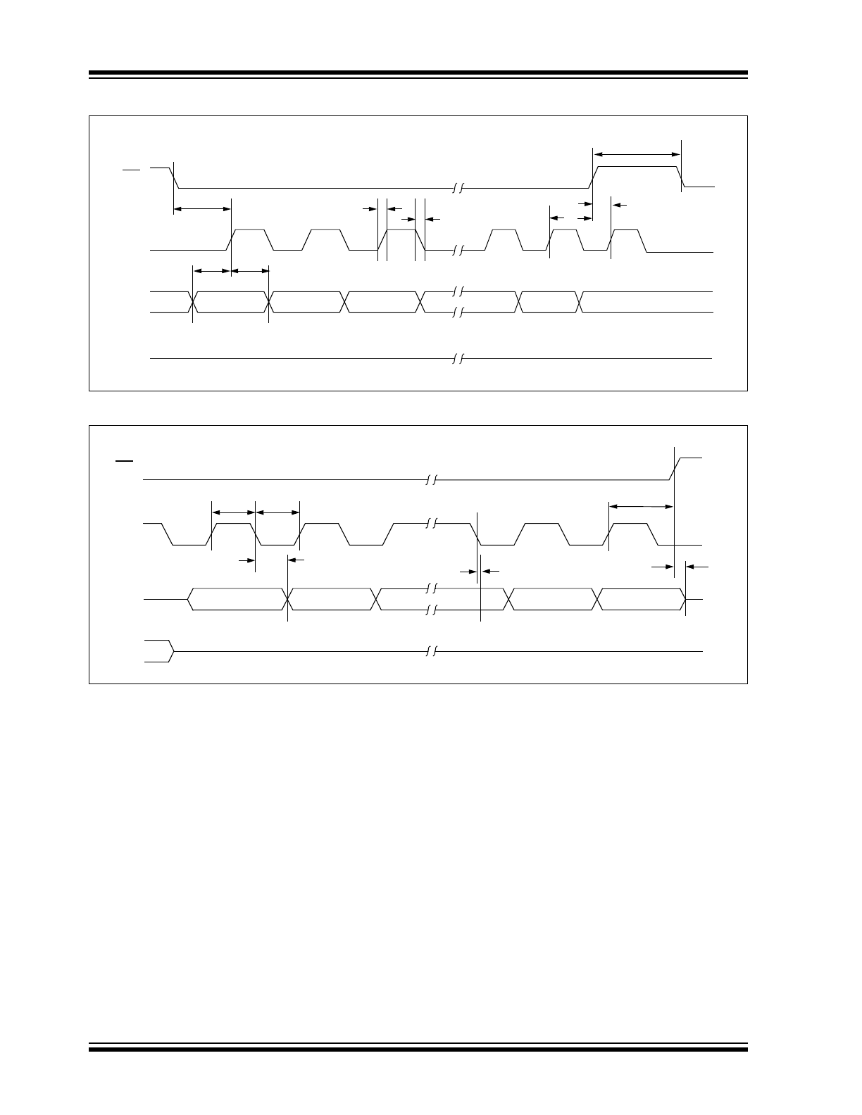
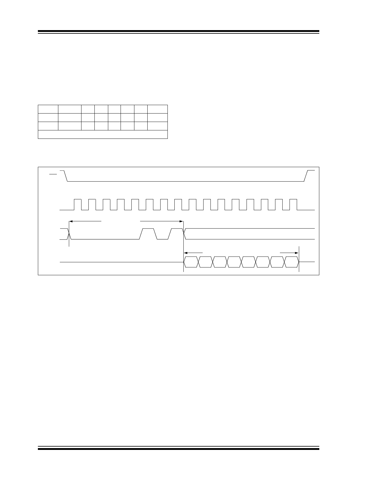
FIGURE 1-1:
SERIAL INPUT TIMING (SPI MODE)
FIGURE 1-2:
SERIAL OUTPUT TIMING (SPI MODE)
CS
SCK
SI
SO
6
5
8
7
11
3
LSB in
MSB in
High-Impedance
2
4
CS
SCK
SO
10
9
12
MSB out
LSB out
3
14
Don’t Care
SI
13

2012 Microchip Technology Inc.
Preliminary
DS25157A-page 5
23LCV512
2.0
FUNCTIONAL DESCRIPTION
2.1
Principles of Operation
The 23LCV512 is an 512 Kbit Serial SRAM designed to
interface directly with the Serial Peripheral Interface
(SPI) port of many of today’s popular microcontroller
families, including Microchip’s PIC
®
microcontrollers. It
may also interface with microcontrollers that do not
have a built-in SPI port by using discrete I/O lines pro-
grammed properly in firmware to match the SPI proto-
col. In addition, the 23LCV512 is also capable of
operating in SDI (or dual SPI) mode.
The 23LCV512 contains an 8-bit instruction register.
The device is accessed via the SI pin, with data being
clocked in on the rising edge of SCK. The CS pin must
be low for the entire operation.
Table 2-1
contains a list of the possible instruction
bytes and format for device operation. All instructions,
addresses and data are transferred MSB first, LSB last.
2.2
Modes of Operation
The 23LCV512 has three modes of operation that are
selected by setting bits 7 and 6 in the MODE register.
The modes of operation are Byte, Page and Burst.
Byte Operation – is selected when bits 7 and 6 in the
MODE register are set to 00. In this mode, the read/
write operations are limited to only one byte. The
command followed by the 16-bit address is clocked into
the device and the data to/from the device is transferred
on the next eight clocks (
Figure 2-1
,
Figure 2-2
).
Page Operation – is selected when bits 7 and 6 in the
MODE register are set to 10. The 23LCV512 has 2048
pages of 32 bytes. In this mode, the read and write oper-
ations are limited to within the addressed page (the
address is automatically incremented internally). If the
data being read or written reaches the page boundary,
then the internal address counter will increment to the
start of the page (
Figure 2-3
,
Figure 2-4
).
Sequential Operation – is selected when bits 7 and 6
in the MODE register are set to 01. Sequential opera-
tion allows the entire array to be written to and read
from. The internal address counter is automatically
incremented and page boundaries are ignored. When
the internal address counter reaches the end of the
array, the address counter will roll over to 0x0000
(
Figure 2-5
,
Figure 2-6
).
2.3
Read Sequence
The device is selected by pulling CS low. The 8-bit
READ instruction is transmitted to the 23LCV512
followed by the 16-bit address. After the correct READ
instruction and address are sent, the data stored in the
memory at the selected address is shifted out on the
SO pin.
If operating in Sequential mode, the data stored in the
memory at the next address can be read sequentially
by continuing to provide clock pulses. The internal
Address Pointer is automatically incremented to the
next higher address after each byte of data is shifted
out. When the highest address is reached (FFFFh),
the address counter rolls over to address 0000h,
allowing the read cycle to be continued indefinitely.
The read operation is terminated by raising the CS
pin.
2.4
Write Sequence
Prior to any attempt to write data to the 23LCV512, the
device must be selected by bringing CS low.
Once the device is selected, the Write command can
be started by issuing a WRITE instruction, followed by
the 16-bit address, and then the data to be written. A
write is terminated by the CS being brought high.
If operating in Page mode, after the initial data byte is
shifted in, additional bytes can be shifted into the
device. The Address Pointer is automatically
incremented. This operation can continue for the entire
page (32 bytes) before data will start to be overwritten.
If operating in Sequential mode, after the initial data
byte is shifted in, additional bytes can be clocked into
the device. The internal Address Pointer is automati-
cally incremented. When the Address Pointer reaches
the highest address (FFFFh), the address counter rolls
over to (0000h). This allows the operation to continue
indefinitely, however, previous data will be overwritten.
23LCV512
DS25157A-page 6
Preliminary
2012 Microchip Technology Inc.
FIGURE 2-1:
BYTE READ SEQUENCE (SPI MODE)
FIGURE 2-2:
BYTE WRITE SEQUENCE (SPI MODE)
TABLE 2-1:
INSTRUCTION SET
Instruction Name Instruction Format
Hex
Code
Description
READ
0000 0011
0x03
Read data from memory array beginning at selected address
WRITE
0000 0010
0x02
Write data to memory array beginning at selected address
EDIO
0011 1011
0x3B
Enter Dual I/O access
RSTIO
1111 1111
0xFF
Reset Dual I/O access
RDMR
0000 0101
0x05
Read Mode Register
WRMR
0000 0001
0x01
Write Mode Register
SO
SI
SCK
CS
0
2
3
4
5
6
7
8
9 10 11
21 22 23 24 25 26 27 28 29 30 31
1
0
1
0
0
0
0
0
1
15 14 13 12
2
1
0
7
6
5
4
3
2
1
0
Instruction
16-bit Address
Data Out
High-Impedance
SO
SI
CS
9 10 11
21 22 23 24 25 26 27 28 29 30 31
0
0
0
0
0
0
0
1
15 14 13 12
2 1
0
7
6
5
4
3
2
1
0
Instruction
16-bit Address
Data Byte
High-Impedance
SCK
0
2
3
4
5
6
7
1
8
2012 Microchip Technology Inc.
Preliminary
DS25157A-page 7
23LCV512
FIGURE 2-3:
PAGE READ SEQUENCE (SPI MODE)
FIGURE 2-4:
PAGE WRITE SEQUENCE (SPI MODE)
7
6
5
4
3
2
1
0
Page X, Word Y
SI
CS
9 10 11
21 22 23 24 25 26 27 28 29 30 31
15 14 13 12
2
1
0
16-bit Address
SCK
0
2
3
4
5
6
7
1
8
SO
CS
7
6
5
4
3
2
1
0
Page X, Word 0
SCK
32
34 35 36 37 38 39
33
7
6
5
4
3
2
1
0
Page X, Word 31
7
6
5
4
3
2
1
0
Page X, Word Y+1
Page X, Word Y
SO
High-Impedance
SI
0
1
0
0
0
0
0
1
Instruction
SI
CS
9 10 11
21 22 23 24 25 26 27 28 29 30 31
15 14 13 12
2
1
0
7
6
5
4
3
2
1
0
16-bit Address
SCK
0
2
3
4
5
6
7
1
8
CS
SI
7
6
5
4
3
2
1
0
Page X, Word 0
7
6
5
4
3
2
1
0
Page X, Word 31
7
6
5
4
3
2
1
0
Page X, Word Y+1
Page X, Word Y
Page X, Word Y
SCK
32
34 35 36 37 38 39
33
0
0
0
0
0
0
0
1
Instruction
23LCV512
DS25157A-page 8
Preliminary
2012 Microchip Technology Inc.
FIGURE 2-5:
SEQUENTIAL READ SEQUENCE (SPI MODE)
SI
CS
9 10 11
21 22 23 24 25 26 27 28 29 30 31
15 14 13 12
2
1
0
7
6
5
4
3
2
1
0
Instruction
16-bit Address
Page X, Word Y
SCK
0
2
3
4
5
6
7
1
8
SO
CS
7
6
5
4
3
2
1
0
Page X+1, Word 1
SCK
7
6
5
4
3
2
1 0
Page X+1, Word 0
7
6
5
4
3
2
1
0
Page X, Word 31
SO
CS
7
6
5
4
3
2
1
0
Page X+n, Word 31
SCK
7
6
5
4
3
2 1
0
Page X+n, Word 1
7
6
5
4
3
2
1
0
Page X+1, Word 31
SO
SI
SI
0
1
0
0
0
0
0
1
2012 Microchip Technology Inc.
Preliminary
DS25157A-page 9
23LCV512
FIGURE 2-6:
SEQUENTIAL WRITE SEQUENCE (SPI MODE)
SI
CS
9 10 11
21 22 23 24 25 26 27 28 29 30 31
0
0
0
0
0
0
0
1
15 14 13 12
2
1
0
7
6
5
4
3
2
1
0
Instruction
16-bit Address
Data Byte 1
SCK
0
2
3
4
5
6
7
1
8
SI
CS
41 42 43
46 47
7
6
5
4
3
2
1
0
Data Byte n
SCK
32
34 35 36 37 38 39
33
40
7
6
5
4
3
2
1
0
Data Byte 3
7
6
5
4
3
2
1
0
Data Byte 2
44 45
23LCV512
DS25157A-page 10
Preliminary
2012 Microchip Technology Inc.
2.5
Read Mode Register Instruction
(RDMR)
The Read Mode Register instruction (RDMR) provides
access to the MODE register. The MODE register may
be read at any time. The MODE register is formatted as
follows:
TABLE 2-2:
MODE REGISTER
The mode bits indicate the operating mode of the
SRAM. The possible modes of operation are:
0 0 = Byte mode
1 0 = Page mode
0 1 = Sequential mode (default operation)
1 1 = Reserved
Bits 0 through 5 are reserved and should always be set
to ‘0’.
See
Figure 2-7
for the RDMR timing sequence.
FIGURE 2-7:
READ MODE REGISTER TIMING SEQUENCE (RDMR)
7
6
5
4
3
2
1
0
W/R
W/R
–
–
–
–
–
–
MODE MODE
0
0
0
0
0
0
W/R = writable/readable
SO
SI
CS
9
10
11
12
13
14
15
1
1
0
0
0
0
0
0
7
6
5
4
2
1
0
Instruction
Data from MODE Register
High-Impedance
SCK
0
2
3
4
5
6
7
1
8
3