
© 2007 Microchip Technology Inc.
DS22061A-page 1
MCP1602
Features
• Over 90% Typical Efficiency
• Output Current: Up To 500 mA
• Power-Good Output with 262 ms Delay
• Low Quiescent Current: 45 µA (typical)
• Low Shutdown Current: 0.05 µA (typical)
• Automatic PWM to PFM Mode Transition
• Adjustable Output Voltage:
- 0.8V to 4.5V
• Fixed Output Voltage:
- 1.2V, 1.5V, 1.8V, 2.5V, and 3.3V
• 2.0 MHz Fixed-Frequency PWM (Heavy Load)
• Internally Compensated
• Undervoltage Lockout (UVLO)
• Overtemperture Protection
• Overcurrent Protection
• Space Saving Packages:
- 8-Lead MSOP
- 8-Lead 3x3 DFN
Applications
• Cellular Telephones
• Portable Computers
• Organizers / PDAs
• USB Powered Devices
• Digital Cameras
• Portable Equipment
• +5V or +3.3V Distributed Systems
General Description
The MCP1602 is a high efficient, fully integrated
500 mA synchronous buck regulator with a power-
good monitor. The 2.7V to 5.5V input voltage range and
low quiescent current (45 µA, typical) makes the
MCP1602 ideally suited for applications powered from
1-cell Li-Ion or 2-cell/3-cell NiMH/NiCd batteries.
At heavy loads, the MCP1602 operates in the 2.0 MHz
fixed frequency PWM mode which provides a low
noise, low output ripple, small-size solution. When the
load is reduced to light levels, the MCP1602
automatically changes operation to a PFM mode to
minimize quiescent current draw from the battery. No
intervention is necessary for a smooth transition from
one mode to another. These two modes of operation
allow the MCP1602 to achieve the highest efficiency
over the entire operating current range.
The open-drain power-good feature of the MCP1602
monitors the output voltage and provides indication
when the output voltage is within 94% (typical) of the
regulation value. The typical 2% hystereses in the
power-good transition threshold as well as a
262 ms (typical) delay time ensures accurate power-
good signaling.
The MCP1602 is available in either the 8-pin DFN or
MSOP package. It is also available with either an
adjustable or fixed output voltage. The available fixed
output voltage options are 1.2V, 1.5V, 1.8V, 2.5V, and
3.3V.
Additional protection features include: UVLO,
overtemperature, and overcurrent protection.
Package Types
V
IN
V
IN
8
7
6
5
4
3
2
1
SHDN
V
CC
PG
A
GND
V
OUT
/V
FB
L
X
P
GND
8
7
6
5
4
3
2
1
SHDN
V
CC
PG
A
GND
V
OUT
/V
FB
L
X
P
GND
3x3 DFN-8
MSOP-8
2.0 MHz, 500 mA Synchronous Buck Regulator
with Power-Good
MCP1602
DS22061A-page 2
© 2007 Microchip Technology Inc.
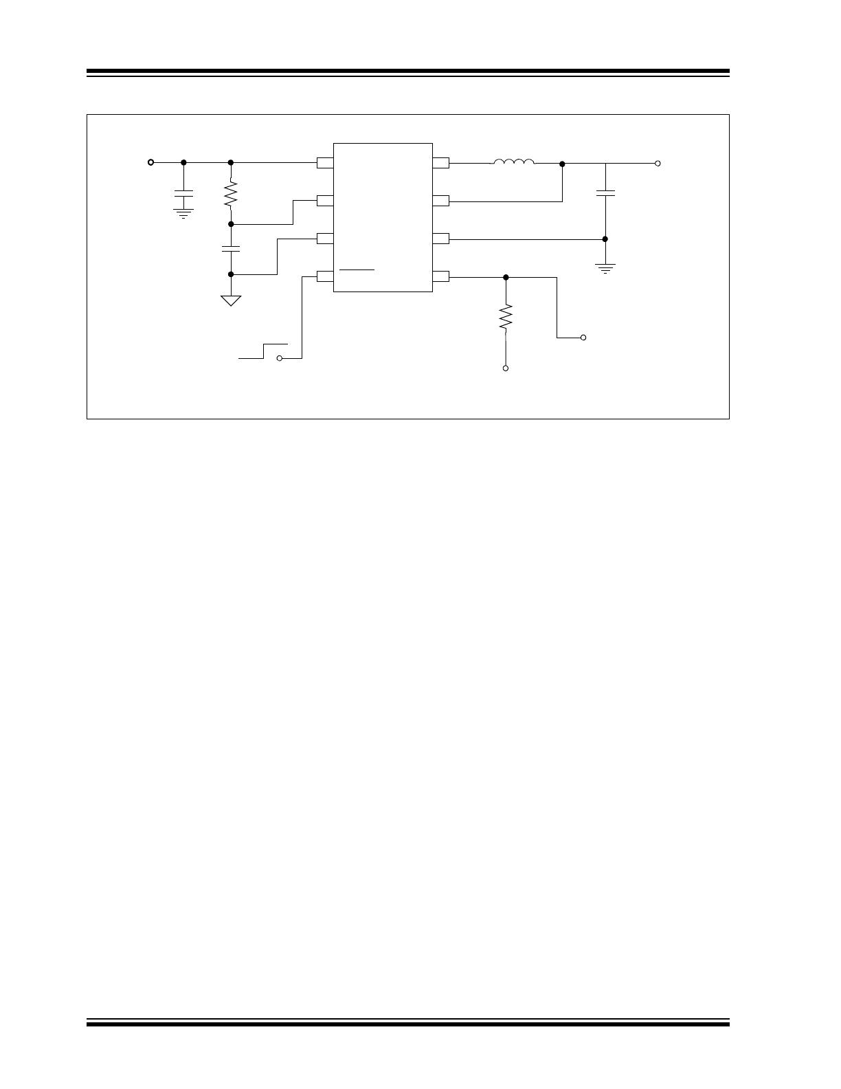
Typical Application Circuit
SHDN
V
CC
PG
A
GND
V
FB
V
IN
L
X
P
GND
1
2
3
4
8
7
6
5
ON
OFF
MCP1602
V
IN
2.7V to 4.5V
V
OUT
1.5V @ 500 mA
V
IN
R
PULLUP
4.7 µF
4.7 µH
4.7 µF
0.1 µF
10
Ω
Processor
Reset
© 2007 Microchip Technology Inc.
DS22061A-page 3
MCP1602
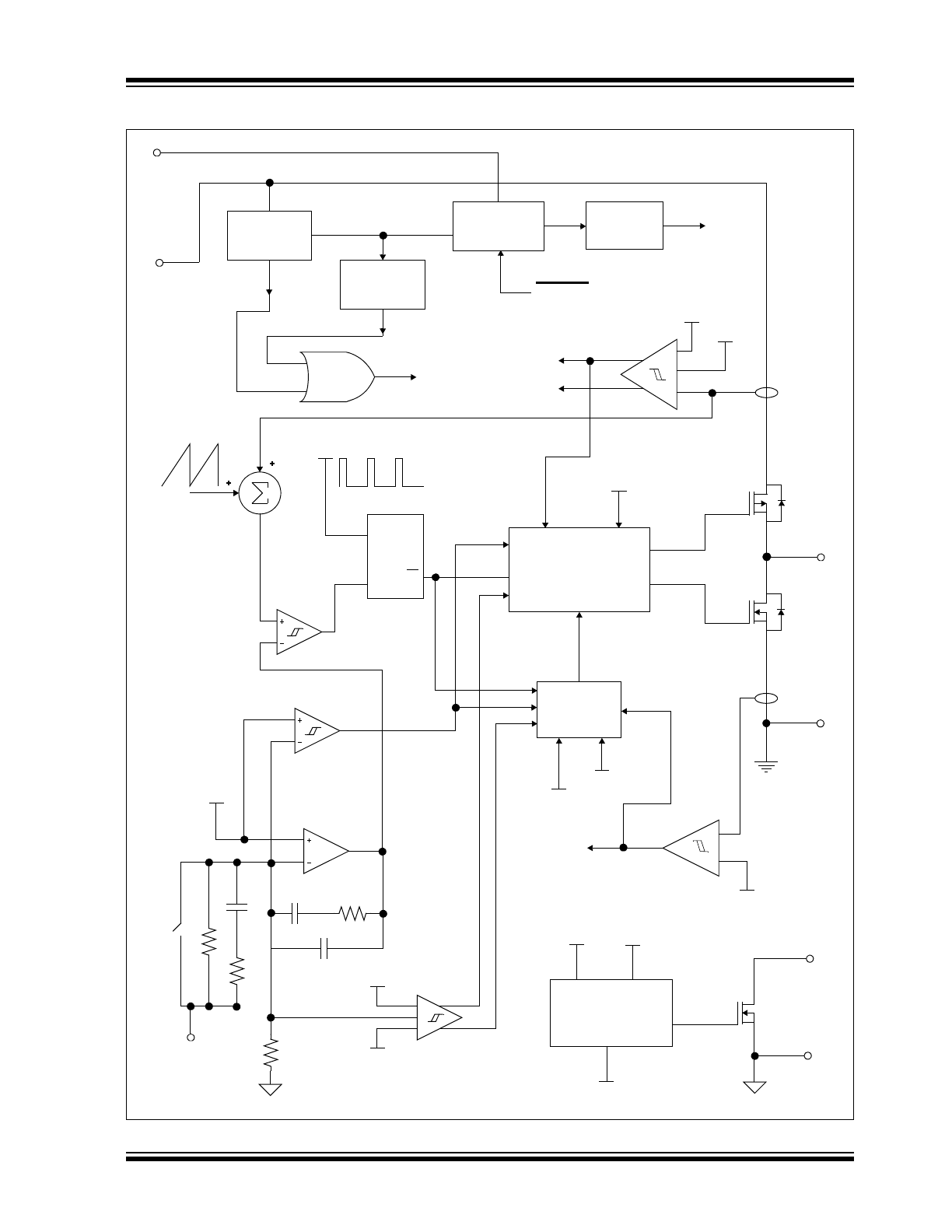
Functional Block Diagram
ILIM
PWM
ILIM
PFM
IPEAK
PWM
IPEAK
PFM
V
IN
SHDN
V
FB
/ V
OUT
P
GND
L
X
Band
Gap
UVLO
Switch Drive
UVLO
V
REF
Logic and Timing
S
R
Q
Q
Soft Start
V
REF
PWM/PFM
Logic
V
REF
Slope
Comp
OSC
-I
PK
Limit
Thermal
Shutdown
TSD
EA
POFF
NOFF
PWM/PFM
PFM Error Amp
PWM Error Amp
OV Threshold
UV Threshold
I
PK
Limit
-ILPK
IPEAK
PWM
IPEAK
PFM
Disable
Switcher
-ILPK
PG Generator
with Delay
V
REF
V
CC
V
OUT
A
GND
PG
V
CC
MCP1602
DS22061A-page 4
© 2007 Microchip Technology Inc.
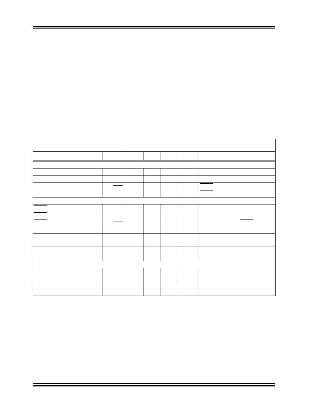
1.0
ELECTRICAL
CHARACTERISTICS
Absolute Maximum Ratings †
V
IN
- A
GND
......................................................................+6.0V
All Other I/O .............................. (A
GND
- 0.3V) to (V
IN
+ 0.3V)
LX to P
GND
............................................. -0.3V to (V
IN
+ 0.3V)
Output Short Circuit Current..................................Continuous
Power Dissipation (Note 6) .......................... Internally Limited
Storage Temperature.................................... -65
o
C to +150
o
C
Ambient Temp. with Power Applied................ -40
o
C to +85
o
C
Operating Junction Temperature.................. -40
o
C to +125
o
C
ESD Protection On All Pins:
HBM..............................................................................3 kV
MM...............................................................................200V
†
Notice: Stresses above those listed under "Maximum
Ratings" may cause permanent damage to the device. This is
a stress rating only and functional operation of the device at
those or any other conditions above those indicated in the
operational sections of this specification is not intended.
Exposure to maximum rating conditions for extended periods
may affect device reliability.
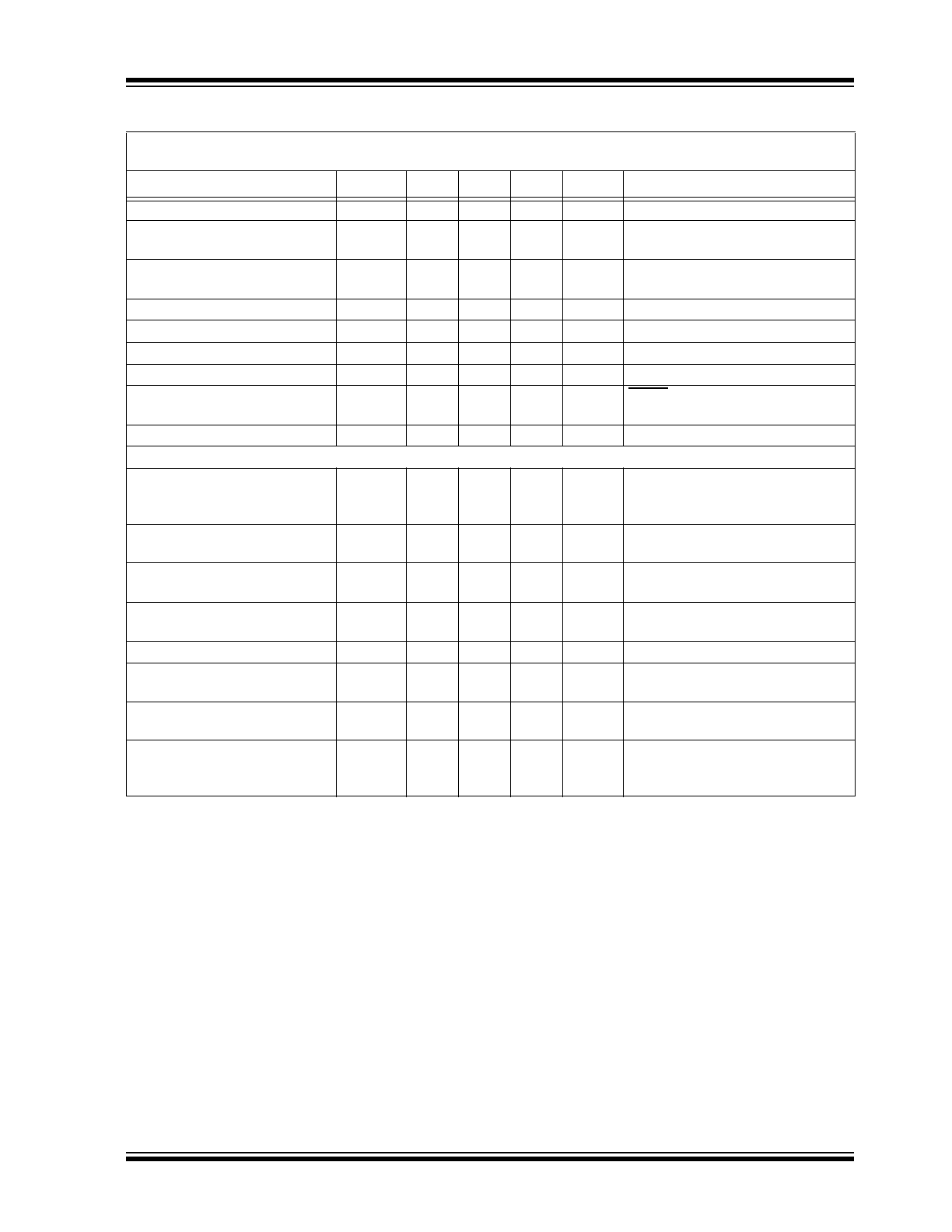
DC CHARACTERISTICS
Electrical Characteristics: Unless otherwise indicated, V
IN
= 3.6V, C
OUT
= C
IN
= 4.7 µF, L = 4.7 µH,
V
OUT
(ADJ) = 1.8V, I
OUT
= 100 mA, T
A
= +25°C.
Boldface specifications apply for the T
A
range of
-40
o
C to +85
o
C.
Parameters
Sym
Min
Typ
Max
Units
Conditions
Input Characteristics
Input Voltage
V
IN
2.7
—
5.5
V
Note 1
Maximum Output Current
I
OUT
500
—
—
mA
Note 1
Shutdown Current
I
IN_SHDN
—
0.05
1
µA
SHDN = GND
Quiescent Current
I
Q
—
45
60
µA
SHDN = V
IN
, I
OUT
= 0 mA
Shutdown/UVLO/Thermal Shutdown Characteristics
SHDN, Logic Input Voltage Low
V
IL
—
—
15
%V
IN
V
IN
= 2.7V to 5.5V
SHDN, Logic Input Voltage High
V
IH
45
—
—
%V
IN
V
IN
= 2.7V to 5.5V
SHDN, Input Leakage Current
V
L_SHND
-1.0
±0.1
1.0
µA
V
IN
= 2.7V to 5.5V, SHDN = A
GND
Undervoltage Lockout
UVLO
2.40
2.55
2.70
V
V
IN
Falling
Undervoltage Lockout Hystere-
sis
UVLO
HYS
—
200
—
mV
Thermal Shutdown
T
SHD
—
150
—
°C
Note 5, Note 6
Thermal Shutdown Hysteresis
T
SHD-HYS
—
10
—
°C
Note 5, Note 6
Output Characteristics
Adjustable Output Voltage
Range
V
OUT
0.8
—
4.5
V
Note 2
Reference Feedback Voltage
V
FB
—
0.8
—
V
Feedback Input Bias Current
I
VFB
—
-1.5
—
nA
Note 1: The minimum V
IN
has to meet two conditions: V
IN
≥ 2.7V and V
IN
≥ V
OUT
+ 0.5V.
2: Reference Feedback Voltage Tolerance applies to adjustable output voltage setting.
3: V
R
is the output voltage setting.
4: Regulation is measured at a constant junction temperature using low duty cycle pulse testing. Load
regulation is tested over a load range of 0.1 mA to the maximum specified output current. Changes in
output voltage due to heating effects are covered by the thermal regulation specification.
5: The maximum allowable power dissipation is a function of ambient temperature, the maximum allowable
temperature and the thermal resistance from junction to air (i.e. T
A
, T
J
,
θ
JA
). Exceeding the maximum
allowable power dissipation causes the device to initiate thermal shutdown.
6: The internal MOSFET switches have an integral diode from the L
X
pin to the V
IN
pin, and from the L
X
pin
to the GND pin. In cases where these diodes are forward-biased, the package power dissipation limits
must be adhered too. Thermal protection is not able to limit the junction temperature for these cases.
7: The current limit threshold is a cycle-by-cycle current limit.
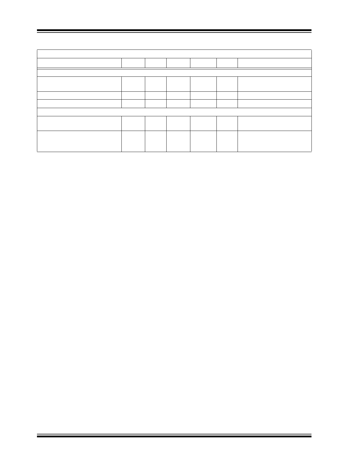
© 2007 Microchip Technology Inc.
DS22061A-page 5
MCP1602
Output Voltage Tolerance Fixed
V
OUT
-2.5
V
R
+2.5
%
Note 3
Line Regulation
V
LINE-
REG
—
0.3
—
%/V
V
IN
= V
R
+ 1V to 5.5V,
I
OUT
= 100 mA
Load Regulation
V
LOAD-
REG
—
0.4
—
%
V
IN
= V
R
+1.5V,
I
LOAD
= 100 mA to 500 mA,
Note 1
Internal Oscillator Frequency
F
OSC
1.6
2.0
2.4
MHz
Start Up Time
T
SS
—
0.5
—
ms
T
R
= 10% to 90%
R
DSon
P-Channel
R
DSon-P
—
450
—
m
Ω
I
P
= 100 mA
R
DSon
N-Channel
R
DSon-N
—
450
—
m
Ω
I
N
= 100 mA
L
X
Pin Leakage Current
I
LX
-1.0
±0.01
1.0
µA
SHDN = 0V, V
IN
= 5.5V, L
X
= 0V,
L
X
= 5.5V
Positive Current Limit Threshold +I
LX(MAX)
—
700
—
mA
Note 7
Power-Good (PG)
Voltage Range
V
PG
1.0
1.2
—
5.5
5.5
V
T
A
= 0°C to +70°C
T
A
= -40°C to +85°C
V
IN
≤ 2.7V, I
SINK
= 100 µA
PG Threshold High
V
TH_H
—
94
96
% of
V
OUT
On Rising V
OUT
PG Threshold Low
V
TH_L
89
92
—
% of
V
OUT
On Falling V
OUT
PG Threshold Hysteresis
V
TH_HYS
—
2
—
% of
V
OUT
PG Threshold Tempco
ΔV
TH
/
ΔT
—
30
—
ppm/°C
PG Delay
t
RPD
—
165
—
µs
V
OUT
= (V
TH_H
+ 100 mV) to
(V
TH_L
- 100 mV)
PG Active Time-out Period
t
RPU
140
262
560
ms
V
OUT
= (V
TH_L
- 100 mV) to
(V
TH_H
+ 100 mV), I
SINK
= 1.2mA
PG Output Voltage Low
PG_V
OL
—
—
0.2
V
V
OUT
= V
TH_L
- 100 mV,
I
PG
= 1.2 mA, V
IN
> 2.7V
I
PG
= 100 µA, 1.0 < V
IN
< 2.7V
DC CHARACTERISTICS (CONTINUED)
Electrical Characteristics: Unless otherwise indicated, V
IN
= 3.6V, C
OUT
= C
IN
= 4.7 µF, L = 4.7 µH,
V
OUT
(ADJ) = 1.8V, I
OUT
= 100 mA, T
A
= +25°C.
Boldface specifications apply for the T
A
range of
-40
o
C to +85
o
C.
Parameters
Sym
Min
Typ
Max
Units
Conditions
Note 1: The minimum V
IN
has to meet two conditions: V
IN
≥ 2.7V and V
IN
≥ V
OUT
+ 0.5V.
2: Reference Feedback Voltage Tolerance applies to adjustable output voltage setting.
3: V
R
is the output voltage setting.
4: Regulation is measured at a constant junction temperature using low duty cycle pulse testing. Load
regulation is tested over a load range of 0.1 mA to the maximum specified output current. Changes in
output voltage due to heating effects are covered by the thermal regulation specification.
5: The maximum allowable power dissipation is a function of ambient temperature, the maximum allowable
temperature and the thermal resistance from junction to air (i.e. T
A
, T
J
,
θ
JA
). Exceeding the maximum
allowable power dissipation causes the device to initiate thermal shutdown.
6: The internal MOSFET switches have an integral diode from the L
X
pin to the V
IN
pin, and from the L
X
pin
to the GND pin. In cases where these diodes are forward-biased, the package power dissipation limits
must be adhered too. Thermal protection is not able to limit the junction temperature for these cases.
7: The current limit threshold is a cycle-by-cycle current limit.
MCP1602
DS22061A-page 6
© 2007 Microchip Technology Inc.
TEMPERATURE SPECIFICATIONS
Electrical Specifications: Unless otherwise indicated, all limits are specified for: V
IN
+ 2.7V to 5.5V
Parameters
Sym
Min
Typ
Max
Units
Conditions
Temperature Ranges
Operating Junction Temperature
Range
T
J
-40
—
+125
°C
Steady State
Storage Temperature Range
T
A
-65
—
+150
°C
Maximum Junction Temperature
T
J
—
—
+150
°C
Transient
Package Thermal Resistances
Thermal Resistance, 8L-MSOP
θ
JA
—
211
—
°C/W
Typical 4-layer Board with
Internal Ground Plane
Thermal Resistance, 8L-3x3 DFN
θ
JA
—
60
—
°C/W
Typical 4-layer Board with
Internal Ground Plane and
2-Vias in Thermal Pad
© 2007 Microchip Technology Inc.
DS22061A-page 7
MCP1602
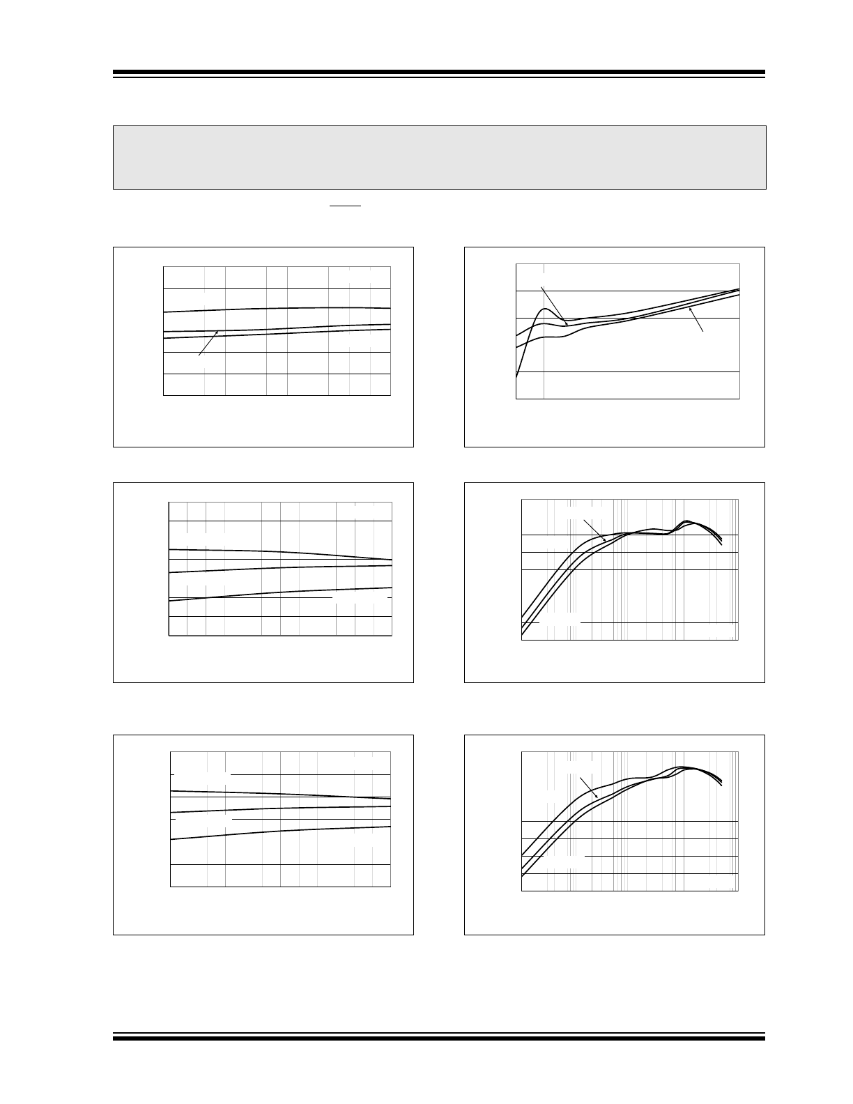
2.0
TYPICAL PERFORMANCE CURVES
Note: Unless otherwise indicated, V
IN
= SHDN = 3.6V, C
OUT
= C
IN
= 4.7 µF, L = 4.7 µH, V
OUT
(ADJ) = 1.8V, I
LOAD
= 100 mA,
T
A
= +25°C. Adjustable or fixed output voltage options can be used to generate the Typical Performance Characteristics.
FIGURE 2-1:
I
Q
vs. Ambient Temperature.
FIGURE 2-2:
Efficiency vs. Input Voltage
(V
OUT
= 1.2V).
FIGURE 2-3:
Efficiency vs. Input Voltage
(V
OUT
= 1.8V).
FIGURE 2-4:
I
Q
vs. Input Voltage.
FIGURE 2-5:
Efficiency vs. Output Load
(V
OUT
= 1.2V).
FIGURE 2-6:
Efficiency vs. Output Load
(V
OUT
= 1.8V).
Note:
The graphs and tables provided following this note are a statistical summary based on a limited number of
samples and are provided for informational purposes only. The performance characteristics listed herein are
not tested or guaranteed. In some graphs or tables, the data presented may be outside the specified
operating range (e.g., outside specified power supply range) and therefore outside the warranted range.
30
35
40
45
50
55
60
-40 -25 -10 5
20 35 50 65 80 95 110 125
Ambient Temperature (
o
C)
Quie
sc
ent Current (µA)
V
OUT
= 1.8V
V
IN
= 5.5V
V
IN
= 3.6V
V
IN
= 4.2V
65
70
75
80
85
90
95
100
3.0
3.2
3.4
3.6
3.8
4.0
4.2
Input Voltage (V)
E
ff
ici
e
n
cy
(%
)
V
OUT
= 1.2V
I
OUT
= 100 mA
I
OUT
= 500 mA
I
OUT
= 300 mA
70
75
80
85
90
95
100
3.0
3.2
3.4
3.6
3.8
4.0
4.2
Input Voltage (V)
E
ff
ici
e
n
cy
(%
)
V
OUT
= 1.8V
I
OUT
= 100 mA
I
OUT
= 500 mA
I
OUT
= 300 mA
30
35
40
45
50
55
2.7
3.05
3.4
3.75
4.1
4.45
4.8
5.15
5.5
Input Voltage (V)
Q
u
ie
sc
ent
Cur
re
nt (
µ
A)
T
A
= +90°C
T
A
= +25°C
T
A
= -40°C
20
30
40
50
60
70
80
90
100
0.1
1
10
100
1000
Output Current (mA)
E
ff
ici
e
n
cy (
%
)
V
OUT
= 1.2V
V
IN
= 3.0V
V
IN
= 3.6V
V
IN
= 4.2V
20
30
40
50
60
70
80
90
100
0.1
1
10
100
1000
Output Current (mA)
E
ff
icie
n
cy
(%)
V
OUT
= 1.8V
V
IN
= 3.0V
V
IN
= 3.6V
V
IN
= 4.2V
MCP1602
DS22061A-page 8
© 2007 Microchip Technology Inc.
Typical Performance Curves (Continued)
Note: Unless otherwise indicated, V
IN
= SHDN = 3.6V, C
OUT
= C
IN
= 4.7 µF, L = 4.7 µH, V
OUT
(ADJ) = 1.8V, I
LOAD
= 100 mA,
T
A
= +25°C. Adjustable or fixed output voltage options can be used to generate the Typical Performance Characteristics.
FIGURE 2-7:
Efficiency vs. Input Voltage
(V
OUT
= 3.3V).
FIGURE 2-8:
PG Active Time-out vs.
Ambient Temperature.
FIGURE 2-9:
Feedback Voltage vs.
Ambient Temperature.
FIGURE 2-10:
Efficiency vs. Output Load
(V
OUT
= 3.3V).
FIGURE 2-11:
PG Threshold Voltage vs.
Ambient Temperature.
FIGURE 2-12:
Output Voltage vs. Load
Current (V
OUT
= 1.8V).
85.0
87.5
90.0
92.5
95.0
97.5
100.0
4.2
4.4
4.6
4.8
5.0
5.2
5.4
Input Voltage (V)
Ef
fi
c
iency
(%
)
V
OUT
= 3.3V
I
OUT
= 100 mA
I
OUT
= 500 mA
I
OUT
= 300 mA
200
220
240
260
280
300
320
340
-40 -25 -10 5
20 35 50 65 80 95 110 125
Ambient Temperature (°C)
P
G
A
ctiv
e Tim
e-
O
u
t (m
s)
0.812
0.816
0.820
0.824
0.828
0.832
-4
0
-2
5
-1
0
5
20
35
50
65
80
95
11
0
12
5
Ambient Temperature (°C)
Feedba
ck
Vol
tage
(V
)
20
30
40
50
60
70
80
90
100
0.1
1
10
100
1000
Output Current (mA)
Ef
fi
c
iency
(%
)
V
OUT
= 3.3V
V
IN
= 5.5V
V
IN
= 4.2V
88
89
90
91
92
93
94
95
96
-40 -25 -10 5
20 35 50 65 80 95 110 125
Ambient Temperature (°C)
PG Thr
eshold (
%
of V
OUT
)
PG Threshold High
PG Threshold Low
1.81
1.82
1.83
1.84
1.85
0
50 100 150 200 250 300 350 400 450 500
Output Current (mA)
Output
V
o
lt
age (V)
© 2007 Microchip Technology Inc.
DS22061A-page 9
MCP1602
Typical Performance Curves (Continued)
Note: Unless otherwise indicated, V
IN
= SHDN = 3.6V, C
OUT
= C
IN
= 4.7 µF, L = 4.7 µH, V
OUT
(ADJ) = 1.8V, I
LOAD
= 100 mA,
T
A
= +25°C. Adjustable or fixed output voltage options can be used to generate the Typical Performance Characteristics.
FIGURE 2-13:
Switching Frequency vs.
Ambient Temperature.
FIGURE 2-14:
Switch Resistance vs. Input
Voltage.
FIGURE 2-15:
Output Voltage Startup
Waveform.
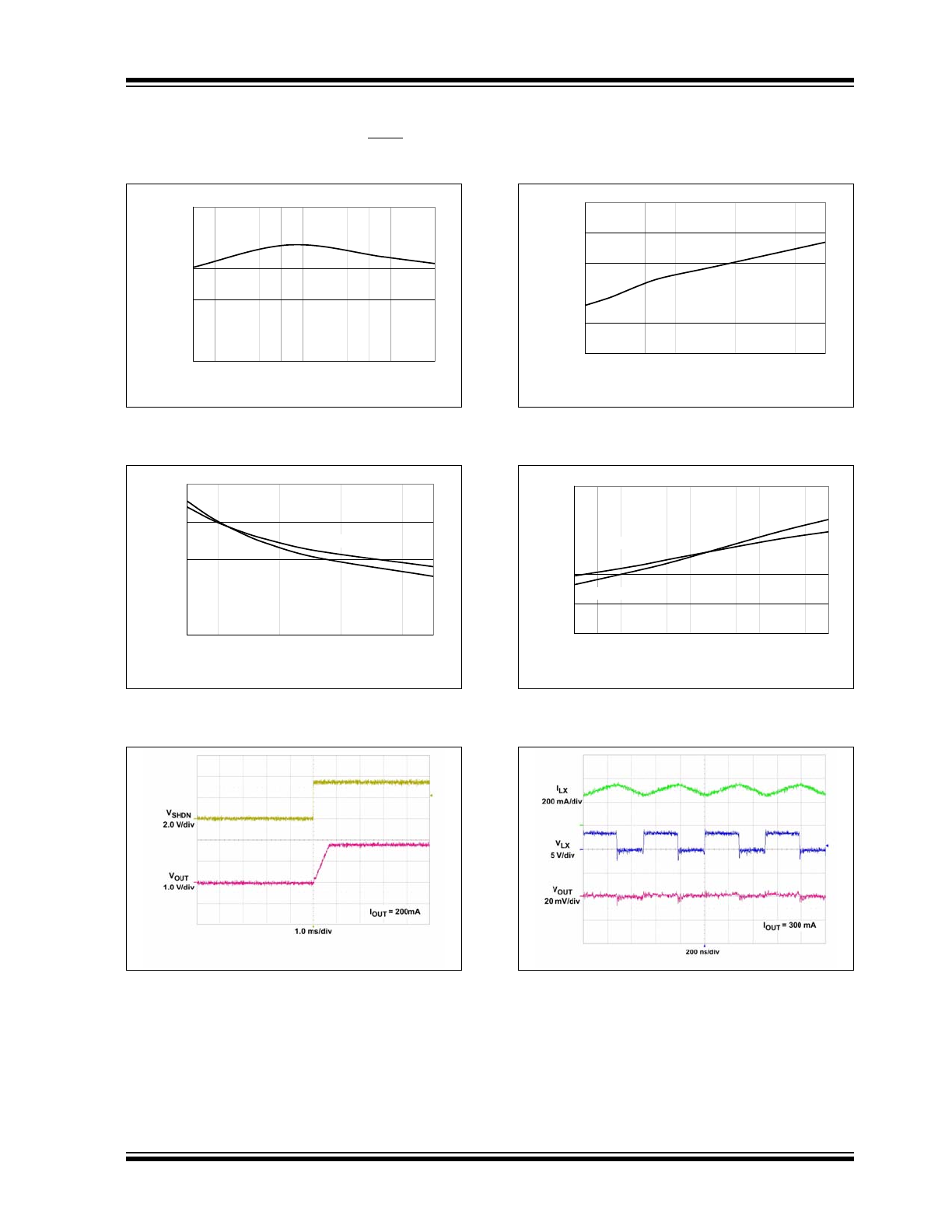
FIGURE 2-16:
Switching Frequency vs.
Input Voltage.
FIGURE 2-17:
Switch Resistance vs.
Ambient Temperature.
FIGURE 2-18:
Heavy Load Switching
Waveform.
1.90
1.92
1.94
1.96
1.98
2.00
-40 -25 -10 5
20 35 50 65 80 95 110 125
Ambient Temperature (°C)
S
w
it
ching Frequency (
M
Hz)
0.2
0.3
0.4
0.5
0.6
2.70 3.05 3.40 3.75 4.10 4.45 4.80 5.15 5.50
Input Voltage (V)
Sw
it
ch Res
ist
anc
e (
Ω
)
N-Channel
P-Channel
1.85
1.90
1.95
2.00
2.05
2.10
2.70 3.05 3.40 3.75 4.10 4.45 4.80 5.15 5.50
Input Voltage (V)
S
w
itching Frequency (
M
Hz)
0.2
0.3
0.4
0.5
0.6
0.7
-40 -25 -10
5
20 35 50 65 80 95 110 125
Ambient Temperature (°C)
Switch
R
esist
an
ce (
Ω
)
N-Channel
P-Channel
MCP1602
DS22061A-page 10
© 2007 Microchip Technology Inc.
Typical Performance Curves (Continued)
Note: Unless otherwise indicated, V
IN
= SHDN = 3.6V, C
OUT
= C
IN
= 4.7 µF, L = 4.7 µH, V
OUT
(ADJ) = 1.8V, I
LOAD
= 100 mA,
T
A
= +25°C. Adjustable or fixed output voltage options can be used to generate the Typical Performance Characteristics.
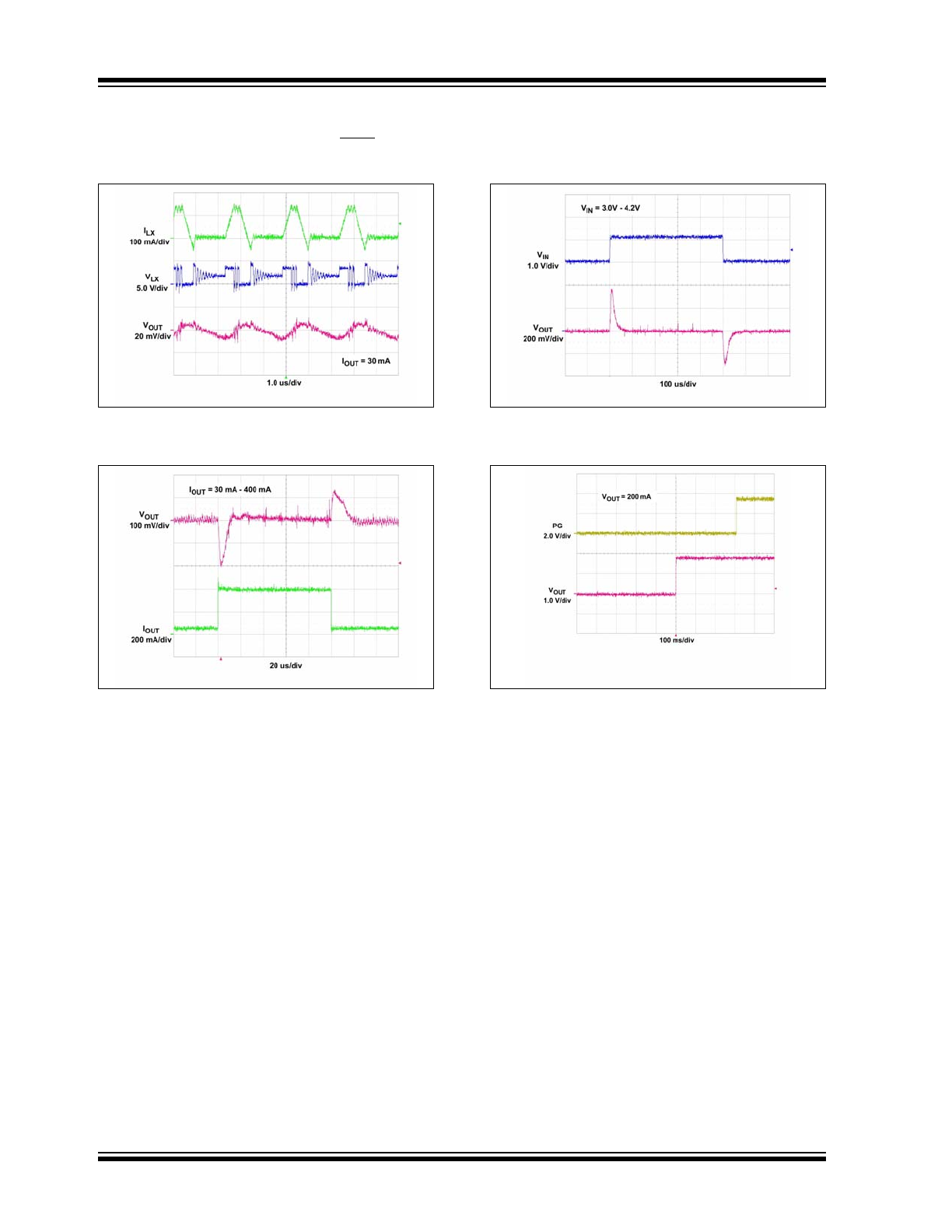
FIGURE 2-19:
Light Load Switching
Waveform.
FIGURE 2-20:
Output Voltage Load Step
Response vs. Time.
FIGURE 2-21:
Output Voltage Line Step
Response vs. Time.
FIGURE 2-22:
Power-Good Output Timing.