
2006-2013 Microchip Technology Inc.
DS21989B-page 1
MCP1256/7/8/9
Features
• Inductorless 1.5x, 2x Boost DC/DC Converter
• Output Voltage: 3.3V
• High Output Voltage Accuracy:
- ±3.0% (V
OUT
Fixed)
• Output Current Up To 100 mA
• 20 mV
PP
Output Voltage Ripple
• Thermal Shutdown and Short Circuit Protection
• Uses Small Ceramic Capacitors
• Switching Frequency: 650 kHz
• Low-Power SLEEP Mode: MCP1256/7
• BYPASS Mode: MCP1258/9
• Low-Power Shutdown Mode: 0.1 µA (Typical)
• Shutdown Input Compatible with 1.8V Logic
• V
IN
Range: 1.8V to 3.6V
• Soft-Start Circuitry to Minimize Inrush Current
• Temperature Range: -40°C to +125°C
• Packaging:
- 10-Pin, 3 mm x 3 mm DFN
- 10-Pin, MSOP
Applications
• Pagers
• Portable Measurement Instruments
• Home Automation Products
• PIC
®
MCU Bias
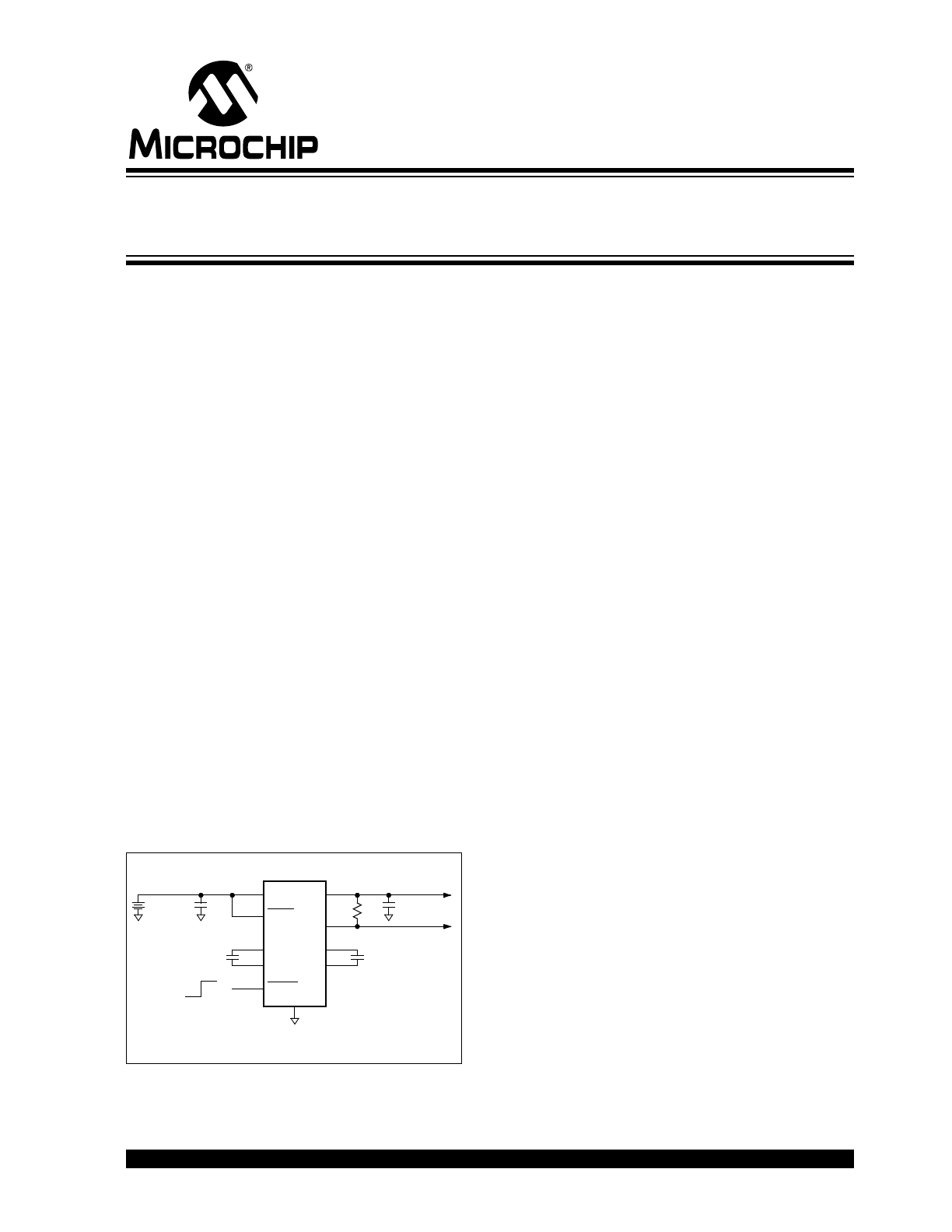
Typical Application
Description
The MCP1256, MCP1257, MCP1258 and MCP1259
are inductorless, positive regulated charge pump
DC/DC converters. The devices generate a regulated
3.3V output voltage from a 1.8V to 3.6V input. The
devices are specifically designed for applications
operating from 2-cell alkaline, Ni-Cd, or Ni-MH
batteries or by one primary lithium MnO2 (or similar)
coin cell battery.
The MCP1256, MCP1257, MCP1258 and MCP1259
provide high efficiency by automatically switching
between 1.5x and 2x boost operation. In addition, at
light output loads, the MCP1256 and MCP1257 can be
placed in a SLEEP mode, lowering the quiescent
current while maintaining the regulated output voltage.
Alternatively, the MCP1258 and MCP1259 provide a
BYPASS feature connecting the input voltage to the
output. This allows for real-time clocks,
microcontrollers or other system devices to remain
biased with virtually no current being consumed by the
MCP1258 or MPC1259.
In normal operation, the output voltage ripple is below
20 mV
PP
at load currents up to 100 mA. Normal opera-
tion occurs at a fixed switching frequency of 650 kHz,
avoiding interference with sensitive IF bands.
The MCP1256 and MCP1258 feature a power-good
output that can be used to detect out-of-regulation
conditions. The MCP1257 and MCP1259 feature a low-
battery indication that issues a warning if the input
voltage drops below a preset voltage threshold.
Extremely low supply current and few external parts (4
capacitors) make these devices ideal for small, battery-
powered applications. A Shutdown mode is also
provided for further power reduction.
The devices incorporate thermal and short-circuit pro-
tection. Two package offerings are provided: 10-pin
MSOP and 10-lead 3 mm x 3 mm DFN. The devices
are completely characterized over the junction temper-
ature range of -40°C to +125°C.
PGOOD
GND
SHDN
1
2
3
4
MCP1256
V
OUT
5
6
7
8
9
10
V
IN
SLEEP
C
IN
10 µF
C
OUT
10 µF
C
1
-
C
1
+
C
1
1 µF
C
2
-
C
2
+
C
2
1 µF
R
1
INPUT
1.8V to 3.6V
OUTPUT
3.3V
Power-Good
Indication
ON / OFF
Typical Application with Power-Good Indication
Regulated 3.3V, Low-Ripple Charge Pump with Low-
Operating Current SLEEP Mode or BYPASS Mode
MCP1256/7/8/9
DS21989B-page 2
2006-2013 Microchip Technology Inc.
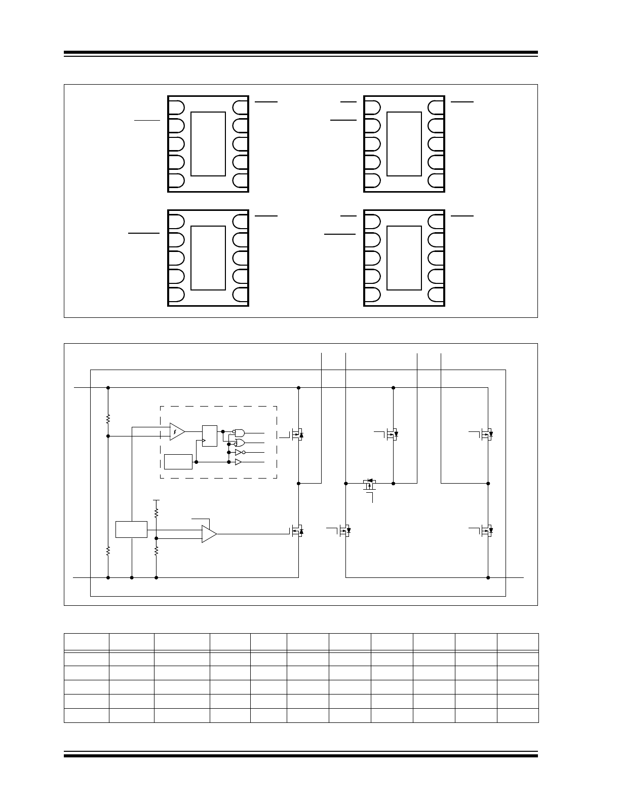
Package Pinouts
Functional Block Diagram
TABLE 1:
SWITCH LOGIC
PGOOD
1
2
3
4
MCP1258
5
6
7
8
9
10
BYPASS
LBO
1
2
3
4
5
6
7
8
9
10
BYPASS
MCP1259
C
1
-
C
2
-
PGOOD
GND
SHDN
1
2
3
4
MCP1256
C
1
+
V
OUT
C
2
+
5
6
7
8
9
10
V
IN
SLEEP
LBO
1
2
3
4
5
6
7
8
9
10
SLEEP
MCP1257
C
2
-
C
1
+
V
OUT
C
2
-
C
1
+
V
OUT
C
2
-
C
1
+
V
OUT
C
1
-
GND
SHDN
C
2
+
VIN
C
1
-
GND
SHDN
C
2
+
V
IN
C
1
-
GND
SHDN
C
2
+
V
IN
S1
S2
S3
S4
S5
S7
S6
+
-
1.5x, 2x Mode
Comparator
840 k
720k
D Q
S5,S7
S6
S4
S1,S3,CE
Gate Drives
V
IN
C
2
-
C
2
+
C
1
-
C
1
+
V
OUT
GND
480 k
840 k
+
-
Feedback
Amplifier
V
OUT
CE
Bandgap
Ref.
650 kHz
Osc.
Mode
Phase
Oscillator
Q
S1
S2(CE)
S3
S4
S5
S6
S7
1.5x
Charging
H
L
H
H
H
L
H
L
H
1.5x
Transfer
L
L
L
L
L
H
L
H
L
2x
Charging
H
H
H
H
H
L
L
H
L
2x
Transfer
L
H
L
L
L
H
L
H
L
BYPASS
—
—
—
H
L
H
H
H
L
L
Legend: L is Logic Low, H is Logic High
2006-2013 Microchip Technology Inc.
DS21989B-page 3
MCP1256/7/8/9
1.0
ELECTRICAL
CHARACTERISTICS
Absolute Maximum Ratings†
Power Supply Voltage, V
IN
...............................................3.8V
Voltage on Any Pin w.r.t. GND ................. -0.3V to (V
IN
+0.3V)
Output Short Circuit Duration ................................continuous
Storage Temperature Range .........................-65°C to +150°C
Ambient Temperature with Power Applied ....-55°C to +125°C
Maximum Junction Temperature ................................. +150°C
ESD protection on all pins
Human Body Model (1.5 k
in Series with 100 pF)2 kV
Machine Model (200 pF, No Series Resistance) .............200V
† Notice: Stresses above those listed under “Maximum
Ratings” may cause permanent damage to the device. This is
a stress rating only and functional operation of the device at
those or any other conditions above those indicated in the
operational listings of this specification is not implied.
Exposure to maximum rating conditions for extended periods
may affect device reliability.
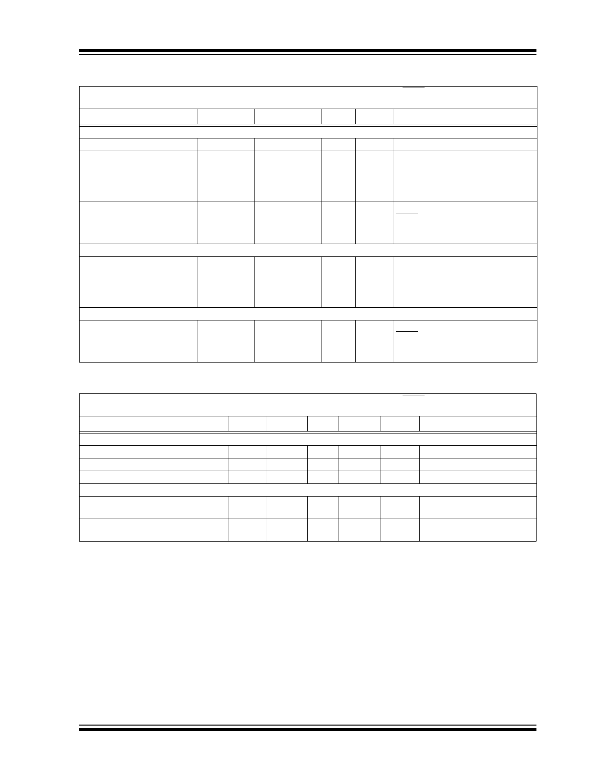
DC CHARACTERISTICS
Electrical Specifications: Unless otherwise indicated, all limits apply for V
IN
= 1.8V to 3.6V, SHDN = V
IN
, C
IN
=
C
OUT
=
10 µF,
C
1
=
C
2
=
1 µF, I
OUT
=
10 mA, T
J
= -40°C to +125°C. Typical values are at T
J
= +25°C.
Parameters
Sym
Min
Typ
Max
Unit
s
Conditions
ALL DEVICES
Supply Voltage
V
IN
1.8
—
3.6
V
Output Voltage
V
OUT
—
3.3
—
V
Output Voltage Accuracy
V
OUT
-3.0
±0.5
+3.0
%
I
OUT
= 10 mA to I
OUT(MAX)
Output Current
I
OUT(MAX)
30
—
—
mA
1.8V < V
IN
< 2.0V
70
—
—
mA
2.0V < V
IN
< 2.2V
100
—
—
mA
2.2V < V
IN
< 3.6V
Short Circuit Current
I
SC
—
150
—
mA
V
OUT
= 0V, V
IN
= 1.8V to 3.6V
Power Efficiency
—
84.5
—
%
V
IN
= 1.8V, I
OUT
= 10 mA
—
84.5
—
%
V
IN
= 1.8V, I
OUT
= 50 mA
—
76.4
—
%
V
IN
= 2.0V, I
OUT
= 10 mA
—
80.1
—
%
V
IN
= 2.0V, I
OUT
= 50 mA
—
64.0
—
%
V
IN
= 2.4V, I
OUT
= 10 mA
—
67.1
—
%
V
IN
= 2.4V, I
OUT
= 50 mA
—
67.5
—
%
V
IN
= 2.4V, I
OUT
= 100 mA
—
69.7
—
%
V
IN
= 2.8V, I
OUT
= 10 mA
—
76.0
—
%
V
IN
= 2.8V, I
OUT
= 50 mA
—
76.7
—
%
V
IN
= 2.8V, I
OUT
= 100 mA
—
65.0
—
%
V
IN
= 3.0V, I
OUT
= 10 mA
—
71.0
—
%
V
IN
= 3.0V, I
OUT
= 50 mA
—
71.6
—
%
V
IN
= 3.0V, I
OUT
= 100 mA
Shutdown Input - SHDN
SHDN Input Voltage Low
V
IL(SHDN)
—
—
0.4
V
SHDN Input Voltage High
V
IH(SHDN)
1.4
—
—
V
SHDN Input Leakage
Current
I
LK(SHDN)
—
0.001
0.1
µA
SHDN Quiescent Current
I
Q
—
0.25
2
µA
V
SHDN
= 0V, T
J
= +25°C
Thermal Shutdown
Thermal Shutdown
Threshold
T
J
—
160
—
C
Thermal Shutdown
Hysteresis
T
J(HYS)
—
15
—
C
MCP1256/7/8/9
DS21989B-page 4
2006-2013 Microchip Technology Inc.
MCP1256 and MCP1257 Devices
SLEEP Mode Input - SLEEP
SLEEP Input Voltage Low
V
IL(SLEEP)
—
—
0.4
V
SLEEP Input Voltage High
V
IH(SLEEP)
1.4
—
—
V
SLEEP Input Leakage
Current
I
LK(SLEEP)
—
0.001
0.1
µA
SLEEP Quiescent Current
I
Q
—
10
20
µA
V
SLEEP
= 0V, I
OUT
= 0 mA
MCP1256 and MCP1258 Devices
Power-Good Output - PGOOD
PGOOD Threshold
V
TH
—
93
—
%
Percent of V
OUT
Falling
PGOOD Hysteresis
V
HYS
—
110
—
mV
V
OUT
Rising
PGOOD Output Low
Voltage
V
OL
—
25
100
mV
I
SINK
= 0.5 mA, V
IN
= 1.8V
PGOOD Input Leakage
Current
I
LK(PGOOD)
—
0.02
1
µA
V
PGOOD
= V
IN
MCP1257 and MCP1259
Low-Battery Output - LBO
LBO Threshold
V
TH
—
1.95
—
V
V
IN
Falling
LBO Hysteresis
V
HYS
—
240
—
mV
V
IN
Rising
LBO Output Low Voltage
V
OL
—
25
100
mV
I
SINK
= 0.5 mA, V
IN
= 1.8V
LBO Input Leakage Current
I
LK(LBO)
—
0.02
1
µA
V
LBO
= V
IN
MCP1258 and MCP1259
BYPASS Mode Input - BYPASS
BYPASS Input Voltage Low
V
IL(BYPASS)
—
—
0.4
V
BYPASS Input Voltage
High
V
IH(BYPASS)
1.4
—
—
V
BYPASS Input Leakage
Current
I
LK(BYPASS)
—
0.001
0.1
µA
BYPASS Quiescent
Current
I
Q
—
0.25
2
µA
V
BYPASS
= 0V, I
OUT
= 0 mA,
T
J
= +25°C
BYPASS Input-to-Output
Impedance
R
BYPASS
—
1.5
—
V
IN
= 2.4V
DC CHARACTERISTICS (CONTINUED)
Electrical Specifications: Unless otherwise indicated, all limits apply for V
IN
= 1.8V to 3.6V, SHDN = V
IN
, C
IN
=
C
OUT
=
10 µF,
C
1
=
C
2
=
1 µF, I
OUT
=
10 mA, T
J
= -40°C to +125°C. Typical values are at T
J
= +25°C.
Parameters
Sym
Min
Typ
Max
Unit
s
Conditions
2006-2013 Microchip Technology Inc.
DS21989B-page 5
MCP1256/7/8/9
TEMPERATURE SPECIFICATIONS
AC CHARACTERISTICS
Electrical Specifications: Unless otherwise indicated, all limits apply for V
IN
= 1.8V to 3.6V, SHDN = V
IN
, C
IN
=
C
OUT
=
10 µF,
C
1
=
C
2
=
1 µF, I
OUT
=
10 mA, T
J
= -40°C to +125°C. Typical values are at T
J
= +25°C.
Parameters
Sym
Min
Typ
Max
Units
Conditions
ALL DEVICES
Internal Oscillator Frequency
F
OSC
—
650
—
kHz
Output Voltage Ripple,
V
RIP
—
5
—
mVp-p
C
OUT
= 10 µF, I
OUT
= 10 mA
Normal Operation
—
20
—
mVp-p
C
OUT
= 10 µF, I
OUT
= 100 mA
—
12
—
mVp-p
C
OUT
= 2.2 µF, I
OUT
= 10 mA
—
55
—
mVp-p
C
OUT
= 2.2 µF, I
OUT
= 100 mA
V
OUT
Wake-up Time From
Shutdown
T
WKUP
—
175
—
µs
V
IN
= 3.0V, I
OUT
= 10 mA,
SHDN = V
IH(MIN)
,
V
OUT
from 0 to 90% Nominal Regulated
Output Voltage
MCP1256 and MCP1257
Output Voltage Ripple,
V
RIP
—
40
—
mVp-p
C
OUT
= 10 µF, I
OUT
= 0.1 mA
SLEEP Mode
—
60
—
mVp-p
C
OUT
= 10 µF, I
OUT
= 4 mA
—
40
—
mVp-p
C
OUT
= 2.2 µF, I
OUT
= 0.1 mA
—
60
—
mVp-p
C
OUT
= 2.2 µF, I
OUT
= 4 mA
MCP1258 and MCP1259
V
OUT
Wake-up Time From
BYPASS
T
WKUP
—
150
—
µs
V
IN
= 3.0V, I
OUT
= 10 mA,
SHDN = V
IH(MIN)
,
V
OUT
from 0 to 90% Nominal Regulated
Output Voltage
Electrical Specifications: Unless otherwise indicated, all limits apply for V
IN
= 1.8V to 3.6V, SHDN = V
IN
, C
IN
=
C
OUT
=
10 µF,
C
1
=
C
2
=
1 µF, I
OUT
=
10 mA, T
J
= -40°C to +125°C. Typical values are at T
J
= +25°C.
Parameters
Sym
Min
Typ
Max
Units
Conditions
Temperature Ranges
Specified Temperature Range
T
J
-40
—
+125
°C
Operating Temperature Range
T
J
-40
—
+125
°C
Storage Temperature Range
T
A
-65
—
+150
°C
Thermal Package Resistances
Thermal Resistance, 10-Lead, MSOP
JA
—
200
—
°C/W
4-Layer JC51-7 Standard Board,
Natural Convection
Thermal Resistance, 10-Lead, DFN
3 mm x 3 mm
JA
—
57
—
°C/W
4-Layer JC51-7 Standard Board,
Natural Convection
MCP1256/7/8/9
DS21989B-page 6
2006-2013 Microchip Technology Inc.
2.0
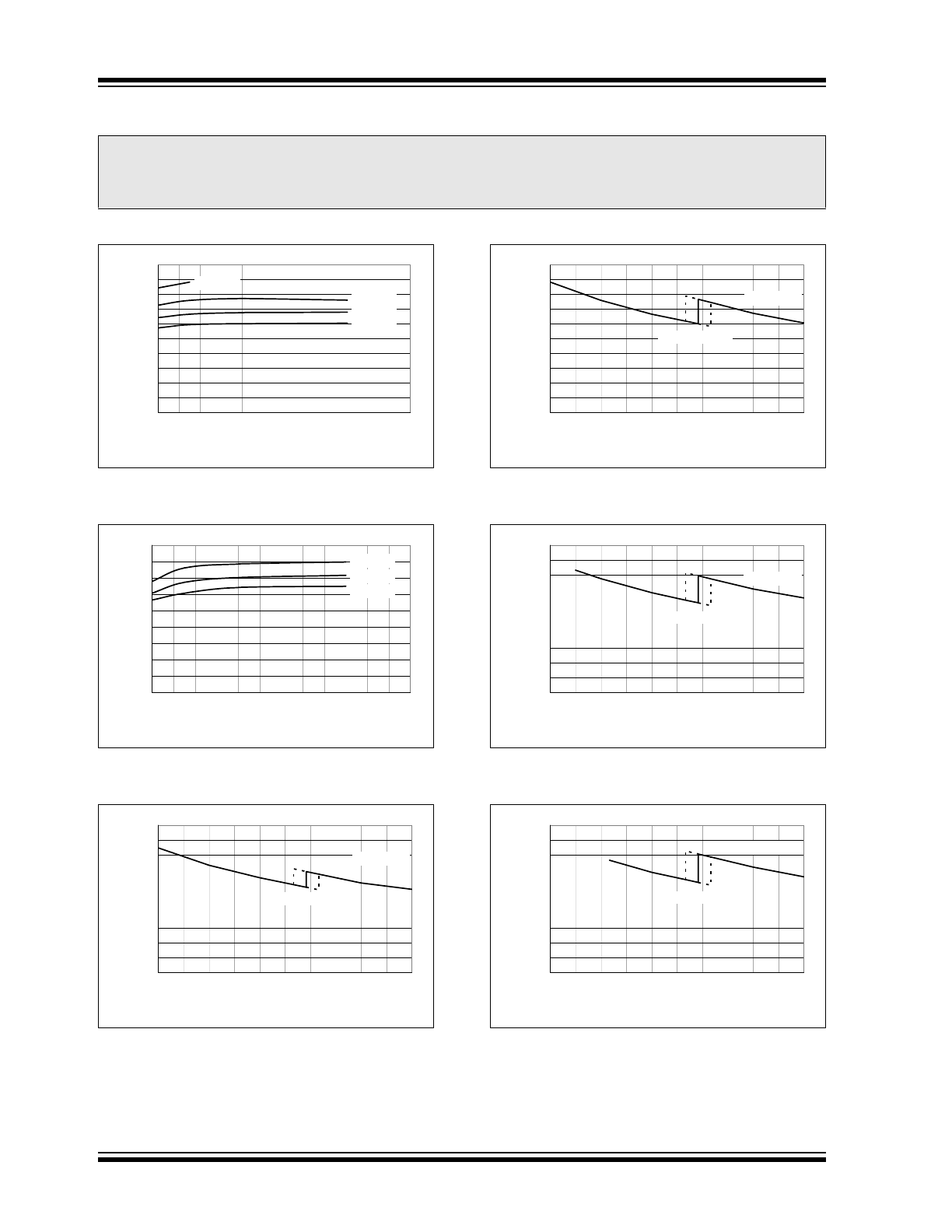
TYPICAL PERFORMANCE CURVES
NOTE: Unless otherwise indicated, C
IN
=
C
OUT
=
10 µF, C
1
=
C
2
=
1 µF, I
OUT
=
10 mA, and T
A
= +25°C.
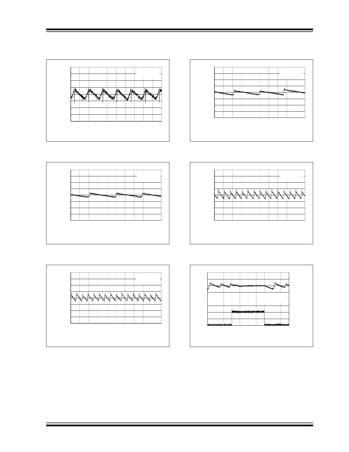
FIGURE 2-1:
Efficiency (
) vs. Output
Current (I
OUT
).
FIGURE 2-2:
Efficiency (
) vs. Output
Current (I
OUT
).
FIGURE 2-3:
Efficiency (
) vs. Supply
Voltage (V
IN
).
FIGURE 2-4:
Efficiency (
) vs. Supply
Voltage (V
IN
).
FIGURE 2-5:
Efficiency (
) vs. Supply
Voltage (V
IN
).
FIGURE 2-6:
Efficiency (
) vs. Supply
Voltage (V
IN
).
Note:
The graphs and tables provided following this note are a statistical summary based on a limited number of
samples and are provided for informational purposes only. The performance characteristics listed herein
are not tested or guaranteed. In some graphs or tables, the data presented may be outside the specified
operating range (e.g., outside specified power supply range) and therefore outside the warranted range.
0
10
20
30
40
50
60
70
80
90
100
10
30
50
70
90
110
130
Output Current (mA)
E
ffi
ci
enc
y
(%
)
V
IN
= 1.8V
V
IN
= 2.1V
V
IN
= 2.4V
V
IN
= 2.7V
0
10
20
30
40
50
60
70
80
90
10
30
50
70
90
110
130
Output Current (mA)
Ef
fi
c
ie
n
c
y
(
%
)
V
IN
= 2.7V
V
IN
= 3.0V
V
IN
= 3.3V
0
10
20
30
40
50
60
70
80
90
100
1.8
2.1
2.4
2.7
3.0
3.3
Input Voltage (V)
E
ffi
ci
en
c
y (%
)
I
OUT
= 10 mA
Mode Transition
0
10
20
30
40
50
60
70
80
90
100
1.8
2.1
2.4
2.7
3.0
3.3
Input Voltage (V)
E
ffi
ci
enc
y
(%
)
I
OUT
= 25 mA
Mode Transition
0
10
20
30
40
50
60
70
80
90
100
1.8
2.1
2.4
2.7
3.0
3.3
Input Voltage (V)
Ef
fi
c
ie
n
c
y
(
%
)
I
OUT
= 50 mA
Mode Transition
0
10
20
30
40
50
60
70
80
90
100
1.8
2.1
2.4
2.7
3.0
3.3
Input Voltage (V)
E
ffi
ci
en
c
y (%
)
I
OUT
= 100 mA
Mode Transition
2006-2013 Microchip Technology Inc.
DS21989B-page 7
MCP1256/7/8/9
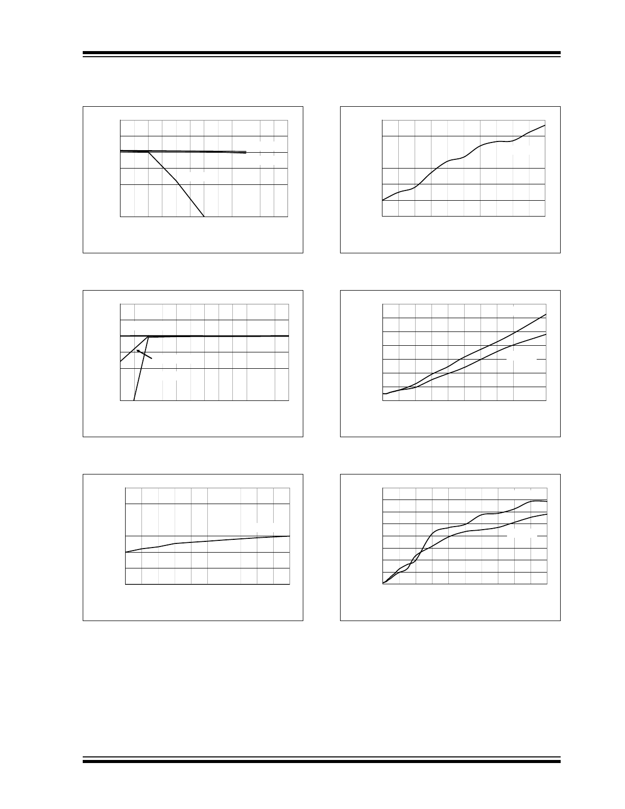
TYPICAL PERFORMANCE CURVES
(CONTINUED)
NOTE: Unless otherwise indicated, C
IN
=
C
OUT
=
10 µF, C
1
=
C
2
=
1 µF, I
OUT
=
10 mA, and T
A
= +25°C.
FIGURE 2-7:
Output Voltage (V
OUT
) vs.
Output Current (I
OUT
).
FIGURE 2-8:
Output Voltage (V
OUT
) vs.
Input Voltage (V
IN
).
FIGURE 2-9:
Quiescent Supply Current
(I
Q
) vs. Output Current (I
OUT
) - Normal Mode.
FIGURE 2-10:
Quiescent Supply Current
(I
Q
) vs. Output Current (I
OUT
) - Normal Mode.
FIGURE 2-11:
Quiescent Supply Current
(I
Q
) vs. Output Current (I
OUT
) - SLEEP Mode.
FIGURE 2-12:
Quiescent Supply Current
(I
Q
) vs. Output Current (I
OUT
) - SLEEP Mode.
2.9
3.0
3.1
3.2
3.3
3.4
3.5
10
30
50
70
90
110
130
Output Current (mA)
O
u
tput
V
o
lt
age (
V
)
V
IN
= 1.8V
V
IN
= 3.6V
V
IN
= 2.1V
2.9
3.0
3.1
3.2
3.3
3.4
3.5
1.8
2.1
2.4
2.7
3.0
3.3
3.6
Input Voltage (V)
Out
put
V
o
lt
ag
e (
V
)
I
OUT
= 10 mA
I
OUT
= 100 mA
I
OUT
= 50 mA
1.2
1.3
1.4
1.5
1.6
1.7
1.8
0
1
2
3
4
5
6
7
8
9
10
Output Current (mA)
Qui
e
sc
ent
S
uppl
y
C
u
rr
ent
(m
A)
V
IN
= 2.4V
1.2
1.4
1.6
1.8
2.0
2.2
2.4
0
10
20
30
40
50
60
70
80
90 100
Output Current (mA)
Qui
e
sc
ent
S
uppl
y
C
u
rre
nt
(m
A
)
V
IN
= 2.4V
0
20
40
60
80
100
120
140
0
0.2 0.4 0.6 0.8
1
1.2 1.4 1.6 1.8
2
Output Current (mA)
Qui
esc
ent
S
uppl
y
C
u
rrent
(µ
A
)
V
IN
= 2.4V
V
IN
= 3.0V
0
0.1
0.2
0.3
0.4
0.5
0.6
0.7
0.8
0
2
4
6
8
10
12
14
16
18
20
Output Current (mA)
Q
u
iesce
n
t S
uppl
y C
u
rre
nt
(m
A)
V
IN
= 2.4V
V
IN
= 3.0V
MCP1256/7/8/9
DS21989B-page 8
2006-2013 Microchip Technology Inc.
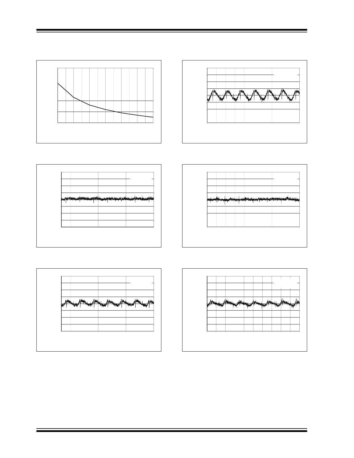
TYPICAL PERFORMANCE CURVES
(CONTINUED)
NOTE: Unless otherwise indicated, C
IN
=
C
OUT
=
10 µF, C
1
=
C
2
=
1 µF, I
OUT
=
10 mA, and T
A
= +25°C.
FIGURE 2-13:
BYPASS Impedance
(R
BYPASS
) vs. Supply Voltage (V
IN
).
FIGURE 2-14:
Output Voltage Ripple vs.
Time - Normal 2x Mode.
FIGURE 2-15:
Output Voltage Ripple vs.
Time - Normal 2x Mode.
FIGURE 2-16:
Output Voltage Ripple vs.
Time - Normal 2x Mode.
FIGURE 2-17:
Output Voltage Ripple vs.
Time - Normal 1.5x Mode.
FIGURE 2-18:
Output Voltage Ripple vs.
Time - Normal 1.5x Mode.
1.0
1.2
1.4
1.6
1.8
2.0
1.8
2.1
2.4
2.7
3.0
3.3
3.6
Input Voltage (V)
B
Y
P
A
S
S
Im
pedanc
e (
Ω
)
-0.04
-0.03
-0.02
-0.01
0.00
0.01
0.02
0.03
0.04
0
1
2
3
4
5
6
7
8
9
10
Time (µs)
O
u
tp
u
t V
o
lt
ag
e
R
ip
p
le (V
)
V
IN
= 2.4V
I
OUT
= 10 mA
-0.04
-0.03
-0.02
-0.01
0.00
0.01
0.02
0.03
0.04
0
1
2
3
4
5
6
7
8
9
10
Time (µs)
O
u
tput
V
o
lt
ag
e R
ippl
e (
V
)
V
IN
= 2.4V
I
OUT
= 50 mA
-0.04
-0.03
-0.02
-0.01
0.00
0.01
0.02
0.03
0.04
0
1
2
3
4
5
6
7
8
9
10
Time (µs)
O
u
tput
V
o
lt
age R
ip
p
le
(
V
)
V
IN
= 2.4V
I
OUT
= 100 mA
-0.04
-0.03
-0.02
-0.01
0.00
0.01
0.02
0.03
0.04
0
1
2
3
4
5
6
7
8
9
10
Time (µs)
O
u
tput
V
o
lt
age R
ip
p
le
(
V
)
V
IN
= 3.0V
I
OUT
= 10 mA
-0.04
-0.03
-0.02
-0.01
0.00
0.01
0.02
0.03
0.04
0
1
2
3
4
5
6
7
8
9
10
Time (µs)
O
u
tput
V
o
lt
ag
e R
ippl
e (
V
)
V
IN
= 3.0V
I
OUT
= 50 mA
2006-2013 Microchip Technology Inc.
DS21989B-page 9
MCP1256/7/8/9
TYPICAL PERFORMANCE CURVES
(CONTINUED)
NOTE: Unless otherwise indicated, C
IN
=
C
OUT
=
10 µF, C
1
=
C
2
=
1 µF, I
OUT
=
10 mA, and T
A
= +25°C.
FIGURE 2-19:
Output Voltage Ripple vs.
Time - Normal 1.5x Mode.
FIGURE 2-20:
Output Voltage Ripple vs.
Time - SLEEP Mode.
FIGURE 2-21:
Output Voltage Ripple vs.
Time - SLEEP Mode.
FIGURE 2-22:
Output Voltage Ripple vs.
Time - SLEEP Mode.
FIGURE 2-23:
Output Voltage Ripple vs.
Time - SLEEP Mode.
FIGURE 2-24:
Output Voltage Ripple vs.
Time - Mode Transition: SLEEP Mode-to-Normal
2x Mode-to-SLEEP Mode.
-0.04
-0.03
-0.02
-0.01
0.00
0.01
0.02
0.03
0.04
0
1
2
3
4
5
6
7
8
9
10
Time (µs)
O
u
tp
u
t V
o
lt
ag
e
R
ip
p
le (V
)
V
IN
= 3.0V
I
OUT
= 100 mA
-0.20
-0.15
-0.10
-0.05
0.00
0.05
0.10
0.15
0.20
0
10
0
20
0
30
0
40
0
50
0
60
0
70
0
80
0
90
0
100
0
Time (µs)
Out
put
V
o
lt
ag
e R
ippl
e (
V
)
V
IN
= 2.4V
I
OUT
= 1 mA
-0.20
-0.15
-0.10
-0.05
0.00
0.05
0.10
0.15
0.20
0
10
0
20
0
30
0
40
0
50
0
60
0
70
0
80
0
90
0
1000
Time (µs)
Out
put
V
o
lt
age R
ippl
e
(V
)
V
IN
= 2.4V
I
OUT
= 10 mA
-0.20
-0.15
-0.10
-0.05
0.00
0.05
0.10
0.15
0.20
0
10
0
20
0
30
0
40
0
50
0
60
0
70
0
80
0
90
0
100
0
Time (µs)
O
u
tput
V
o
lt
age R
ippl
e (
V
)
V
IN
= 3.0V
I
OUT
= 1 mA
-0.20
-0.15
-0.10
-0.05
0.00
0.05
0.10
0.15
0.20
0
10
0
20
0
30
0
40
0
50
0
60
0
70
0
80
0
90
0
100
0
Time (µs)
Out
put
V
o
lt
ag
e R
ippl
e (
V
)
V
IN
= 3.0V
I
OUT
= 10 mA
0
1
2
3
4
5
6
7
8
0
50
100
150
200
250
300
350
400
450
500
Time (µs)
S
L
E
E
P
Input
V
o
lt
ag
e (
V
)
-0.60
-0.50
-0.40
-0.30
-0.20
-0.10
0.00
0.10
0.20
Outp
ut Voltag
e Ripp
le (V)
V
IN
= 2.4V
I
OUT
= 10 mA
MCP1256/7/8/9
DS21989B-page 10
2006-2013 Microchip Technology Inc.
TYPICAL PERFORMANCE CURVES
(CONTINUED)
NOTE: Unless otherwise indicated, C
IN
=
C
OUT
=
10 µF, C
1
=
C
2
=
1 µF, I
OUT
=
10 mA, and T
A
= +25°C.
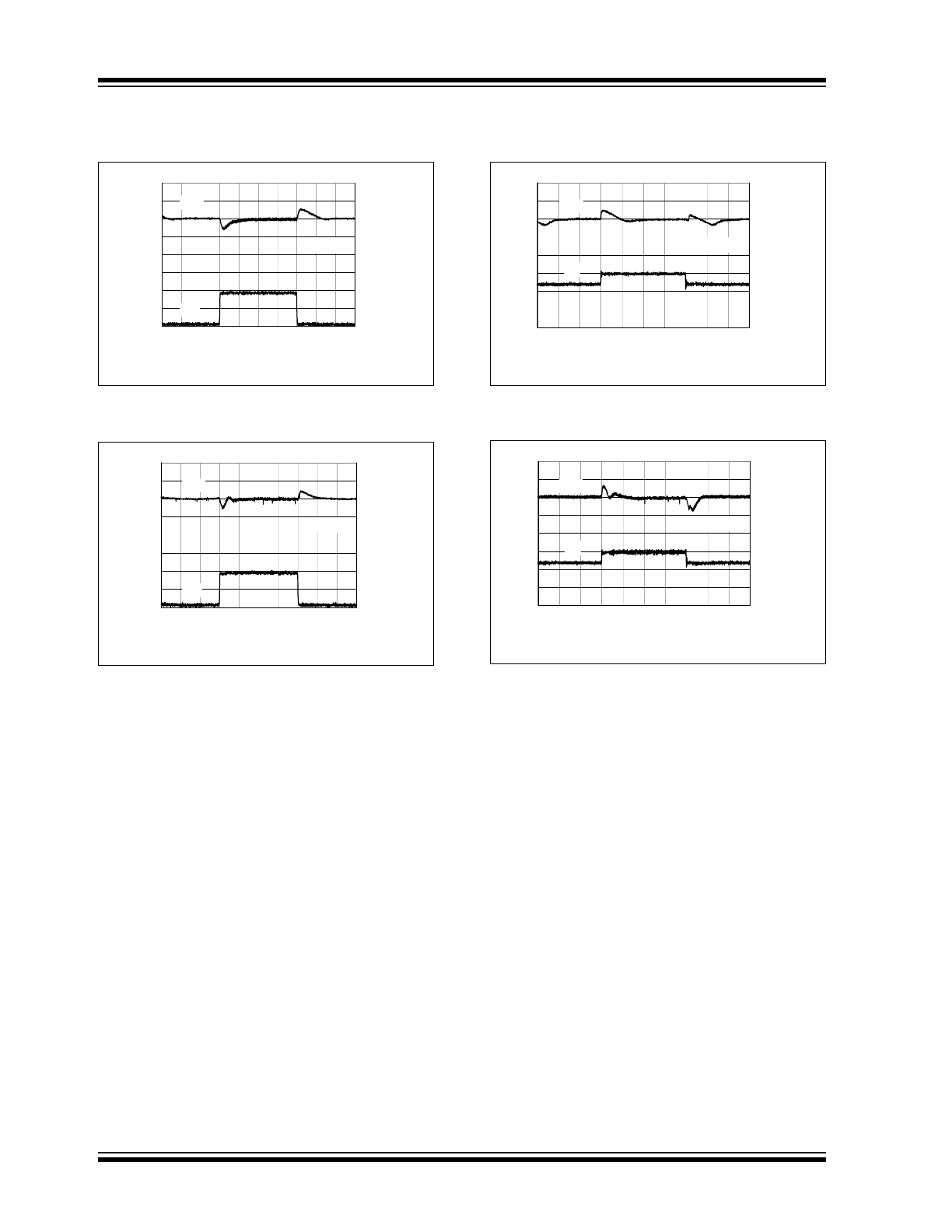
FIGURE 2-25:
Load Transient Response -
Normal 2x Mode.
FIGURE 2-26:
Load Transient Response -
Normal 1.5x Mode.
FIGURE 2-27:
Line Transient Response.
FIGURE 2-28:
Line Transient Response.
0.00
0.05
0.10
0.15
0.20
0.25
0.30
0.35
0.40
0
50
10
0
15
0
20
0
25
0
30
0
35
0
40
0
45
0
50
0
Time (µs)
O
u
tp
u
t C
u
rr
e
n
t (A
)
-0.60
-0.50
-0.40
-0.30
-0.20
-0.10
0.00
0.10
0.20
O
u
tp
u
t V
o
lt
a
g
e R
ipp
le
(V)
V
IN
= 2.4V
V
OUT
I
OUT
0.00
0.05
0.10
0.15
0.20
0.25
0.30
0.35
0.40
0
50
10
0
15
0
20
0
25
0
30
0
35
0
40
0
45
0
50
0
Time (µs)
O
u
tp
ut
C
u
rre
nt
(
A
)
-0.60
-0.50
-0.40
-0.30
-0.20
-0.10
0.00
0.10
0.20
O
u
tp
ut
V
o
lt
ag
e
R
ippl
e
(V
)
V
IN
= 3.0V
V
OUT
I
OUT
0
1
2
3
4
5
6
7
8
0
50
10
0
15
0
20
0
25
0
30
0
35
0
40
0
45
0
50
0
Time (µs)
In
p
u
t V
o
lt
ag
e
(V
)
-0.60
-0.50
-0.40
-0.30
-0.20
-0.10
0.00
0.10
0.20
Ou
tp
ut V
o
lt
ag
e R
ippl
e
(V
)
I
OUT
= 10 mA
V
OUT
V
IN
0
1
2
3
4
5
6
7
8
0
50
100
150
200
250
300
350
400
450
500
Time (µs)
Input
Vol
ta
g
e
(V)
-0.60
-0.50
-0.40
-0.30
-0.20
-0.10
0.00
0.10
0.20
Output
V
o
lt
age R
ippl
e
(V
)
I
OUT
= 100 mA
V
OUT
V
IN