
2005-2013 Microchip Technology Inc.
DS21977C-page 1
MCP9805
Features
• Meets JEDEC Standard JC42.4 for Mobile
Platform Memory Module Thermal Sensor
• Temperature-to-Digital Converter
• Accuracy with 0.25 °C/LSb Resolution:
- ±1°C (max.) from +75°C to +95°C
- ±2°C (max.) from +40°C to +125°C
- ±3°C (max.) from -20°C to +125°C
• Programmable Temperature Monitor Boundary
• Critical Temperature Output
• Operating Voltage Range: 3.0V to 3.6V
• 2-wire Interface: SMBus/Standard mode I
2
C™
Compatible
• Operating Current: 200 µA (typ.)
• Shutdown Current: 0.1 µA (typ.)
• Available Packages: 2x3 DFN-8, TSSOP-8
Typical Applications
• Dual In-line Memory Module (DIMM)
• Personal Computers (PCs) and Servers
• Hard Disk Drives and Other PC Peripherals
• General Purpose Temperature Sensor
Typical Application
Description
Microchip Technology Inc.’s MCP9805 digital tempera-
ture sensor converts temperatures between -40°C and
+125°C to a digital word. This sensor is designed to
meet the JEDEC standard JC42.4 for Mobile Platform
Memory Module Thermal Sensor. This device provides
an accuracy of ±1°C (max.) from a temperature range
of +75°C to +95°C (active range) and ±2°C (max.) from
+40°C to +125°C (monitor range) as defined in the
JEDEC standard.
The MCP9805 comes with user-programmable
registers that provide flexibility for DIMM
temperature-sensing applications. The registers allow
user-selectable settings such as Shutdown or
Low-Power modes and the specification of tempera-
ture event and critical output boundaries. When the
temperature changes beyond the specified boundary
limits, the MCP9805 outputs an Event signal. The user
has the option of setting the Event output signal polarity
as either an active-low or active-high comparator
output for thermostat operation, or as a temperature
event interrupt output for microprocessor-based
systems. The Event output can also be configured as a
critical temperature output.
This sensor has a 2-wire industry-standard SMBus
and Standard mode I
2
C compatible (100 kHz bus
clock) serial interface protocol, allowing up to eight sen-
sors to be controlled in a single serial bus. These fea-
tures make the MCP9805 ideal for sophisticated
multi-zone temperature-monitoring applications.
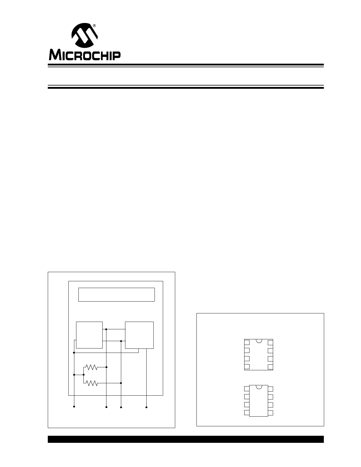
Package Types
Memory
Memory Module
SPD*
Temperature
Sensor
EEPROM
MCP9805
3.3 V
DD_SPD
SDA SCLK
R
R
Event
* Serial Presence Detect
SDA
GND
Event
SCLK
8-Pin DFN (2x3)
A0
V
DD
A1
A2
1
2
3
4
8
7
6
5
SDA
GND
Event
SCLK
MCP9805
1
2
3
4
8-Pin TSSOP
A0
V
DD
A1
A2
8
7
6
5
Memory Module Digital Temperature Sensor
MCP9805
DS21977C-page 2
2005-2013 Microchip Technology Inc.
1.0
ELECTRICAL
CHARACTERISTICS
Absolute Maximum Ratings †
V
DD
....................................................................... 6.0V
Voltage at all Input/Output pins .... GND – 0.3V to 5.5V
Storage temperature ..........................-65°C to +150°C
Ambient temp. with power applied .....-40°C to +125°C
Junction Temperature (T
J
)................................ +150°C
ESD protection on all pins (HBM:MM)....... (4 kV:200V)
Latch-Up Current at each pin ........................ ±200 mA
†Notice: Stresses above those listed under “Maximum
ratings” may cause permanent damage to the device. This is
a stress rating only and functional operation of the device at
those or any other conditions above those indicated in the
operational listings of this specification is not implied.
Exposure to maximum rating conditions for extended periods
may affect device reliability.
DC CHARACTERISTICS
Electrical Specifications: Unless otherwise indicated, V
DD
= 3.0V to 3.6V, GND = Ground and T
A
= -20°C to +125°C.
Parameters
Sym
Min
Typ
Max
Unit
Conditions
Power Supply
Operating Voltage Range
V
DD
3.0
—
3.6
V
Operating Current
I
DD
—
200
500
µA
Continuous Operation
Shutdown Current
I
SHDN
—
0.1
2
µA
Shutdown Mode
Power-On Reset Threshold (POR)
V
POR
—
2.2
—
V
V
DD
Falling Edge
Power Supply Rejection
PSR
DC
—
±0.3
—
°C
PSR
AC
—
±0.5
—
°C
V
DD
= 3.3V + 150 mVpp
(0 to 1 MHz), T
A
= +25°C
Temperature Sensor Accuracy
Accuracy with 0.25 °C/LSb Resolution:
+75°C to +95°C
T
ACY
-1.0
±0.5
+1.0
°C
Active Temp. Range
+40°C to +125°C
T
ACY
-2.0
±1.0
+2.0
°C
Monitor Temp. Range
-20°C to +125°C
T
ACY
-3.0
±2.0
+3.0
°C
T
A
= -40°C
T
ACY
—
±2
—
°C
Internal
ADC
Conversion Time (10-bits + Sign):
0.25 °C/LSb
t
CONV
—
65
125
ms
17 samples/sec. (typ.)
Event Output (Open-Drain)
High-Level Current (leakage)
I
OH
—
—
1
µA
V
OH
= 3.6V
Low-Level Voltage
V
OL
—
—
0.4
V
I
OL
= 3 mA
Thermal Response
Response Time (Note):
DFN
t
RES
—
0.7
—
s
Time to 63% of +22°C (Air)
to +125°C (Oil Bath)
TSSOP
t
RES
—
1.5
—
s
Note:
Thermal response with 1x1 inch dual-sided copper clad.
2005-2013 Microchip Technology Inc.
DS21977C-page 3
MCP9805
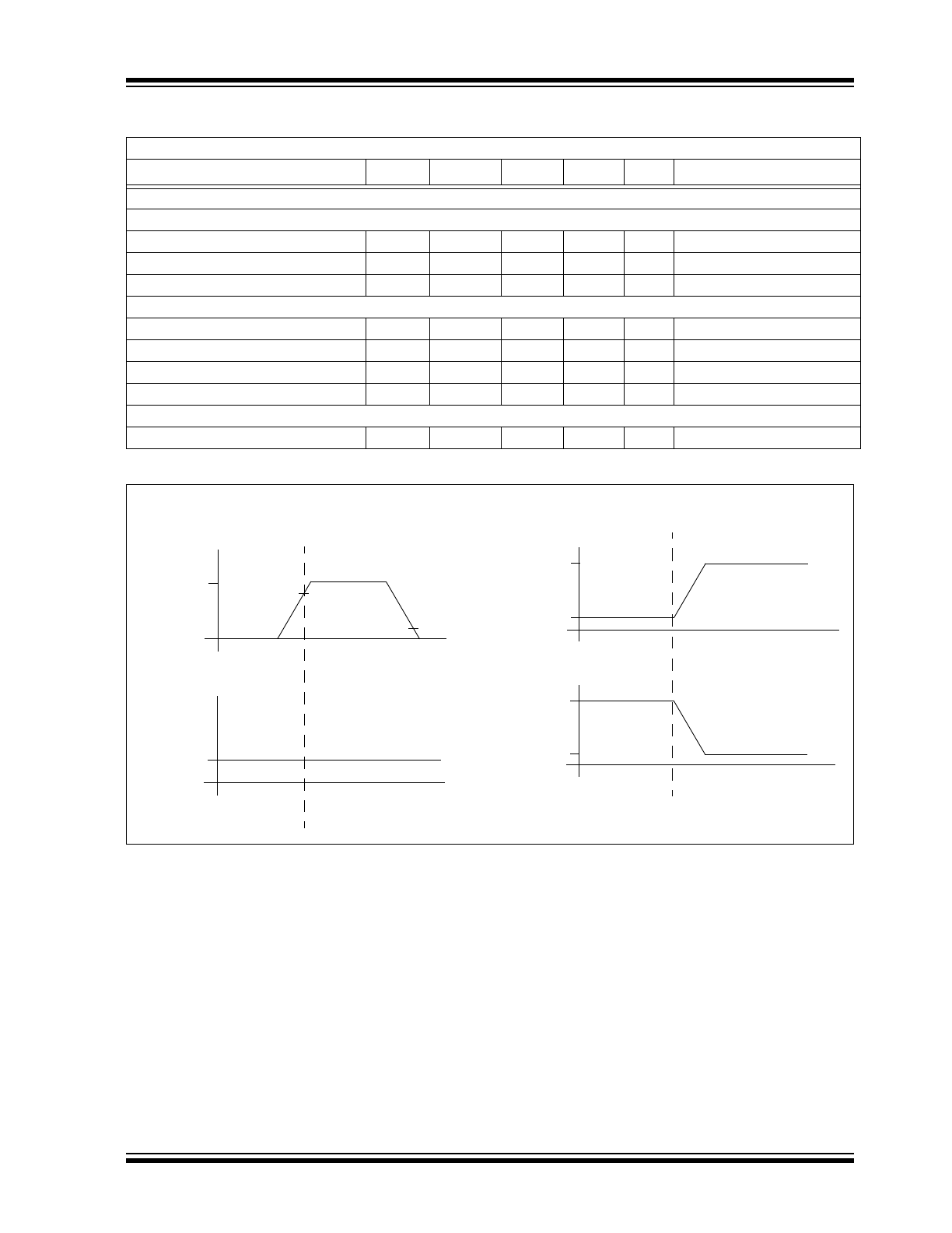
Graphical Symbol Description
DIGITAL INPUT/OUTPUT PIN CHARACTERISTICS
Electrical Specifications: Unless otherwise indicated, V
DD
= 3.0V to 3.6V, GND = Ground and T
A
= -20°C to +125°C.
Parameters
Sym
Min
Typ
Max
Units
Conditions
Serial Input/Output (SCLK, SDA, A0, A1, A2)
Input
High-Level Voltage
V
IH
2.1
—
—
V
Low-Level Voltage
V
IL
—
—
0.8
V
Input Current
I
IN
—
—
±5
µA
Output (SDA)
Low-Level Voltage
V
OL
—
—
0.4
V
I
OL
= 3 mA
High-Level Current (leakage)
I
OH
—
—
1
µA
V
OH
= 3.6V
Low-Level Current
I
OL
6
—
—
mA
V
OL
= 0.6V
Capacitance
C
IN
—
5
—
pF
SDA and SCLK Inputs
Hysteresis
V
HYST
—
0.5
—
V
V
DD
V
IH
V
IL
I
IN
Voltage
Current
time
time
V
DD
I
OH
Voltage
Current
time
time
SDA & SCLK INPUTS
SDA OUTPUT
V
OL
I
OL
MCP9805
DS21977C-page 4
2005-2013 Microchip Technology Inc.
Timing Diagram
SERIAL INTERFACE TIMING CHARACTERISTICS
Electrical Specifications: Unless otherwise indicated, V
DD
= 3.0V to 3.6V, GND = Ground, T
A
= -20°C to +125°C,
C
L
= 80 pF and all limits measured to 50% point.
Parameters
Sym
Min
Typ
Max
Units
Conditions
2-Wire SMBus/Standard Mode I
2
C™ Compatible Interface (Note)
Serial Port Clock Frequency
f
SC
10
—
100
kHz
Low Clock
t
LOW
4.7
—
—
µs
High Clock
t
HIGH
4.0
—
—
µs
Rise Time
t
R
—
—
1000
ns
(V
IL MAX
- 0.15V) to (V
IH MIN
+ 0.15V)
Fall Time
t
F
—
—
300
ns
(V
IH MIN
+ 0.15V) to (V
IL MAX
- 0.15V)
Data Setup Before SCLK High
t
SU-DATA
250
—
—
ns
Data Hold After SCLK Low
t
HD-DATA
300
—
—
ns
Start Condition Setup Time
t
SU-START
4.7
—
—
µs
Start Condition Hold Time
t
HD-START
4.0
—
—
µs
Stop Condition Setup Time
t
SU-STOP
4.0
—
—
µs
Bus Free
t
B-FREE
4.7
—
—
µs
Time Out
t
OUT
25
40
50
ms
Note:
The serial interface specification min./max. limits are specified by characterization (not production tested).
t
SU-START
t
H-START
t
SU-DATA
t
SU-STOP
t
B-FREE
SCLK
SDA
t
H-DATA
t
HIGH
t
LOW
t
OUT
t
R
, t
F
START Condition
Data Transmission
STOP Condition
TEMPERATURE CHARACTERISTICS
Electrical Specifications: Unless otherwise indicated, V
DD
= 3.0V to 3.6V, GND = Ground.
Parameters
Sym
Min
Typ
Max
Units
Conditions
Temperature Ranges
Specified Temperature Range
T
A
-20
—
+125
°C
Operating Temperature Range
T
A
-40
—
+125
°C
Note 1
Storage Temperature Range
T
A
-65
—
+150
°C
Thermal Package Resistances
Thermal Resistance, 8L-DFN
JA
—
41
—
°C/W
Thermal Resistance, 8L-TSSOP
JA
—
123.7
—
°C/W
Note 1:
Operation in this range must not cause T
J
to exceed Maximum Junction Temperature (+150°C).
2005-2013 Microchip Technology Inc.
DS21977C-page 5
MCP9805
2.0
TYPICAL PERFORMANCE CURVES
Note: Unless otherwise noted: V
DD
= 3.0V to 3.6V, GND = Ground, C
de_cap
= 0.1 µF
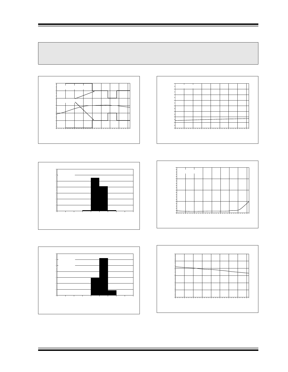
FIGURE 2-1:
Average Temperature
Accuracy.
FIGURE 2-2:
Temperature Accuracy
Histogram, T
A
= +95°C.
FIGURE 2-3:
Temperature Accuracy
Histogram, T
A
= +75°C.
FIGURE 2-4:
Supply Current vs. Ambient
Temperature.
FIGURE 2-5:
Shutdown Current vs.
Ambient Temperature.
FIGURE 2-6:
Power-on Reset Threshold
Voltage vs. Ambient Temperature.
Note:
The graphs and tables provided following this note are a statistical summary based on a limited number of
samples and are provided for informational purposes only. The performance characteristics listed herein
are not tested or guaranteed. In some graphs or tables, the data presented may be outside the specified
operating range (e.g., outside specified power supply range) and therefore outside the warranted range.
-3.0
-2.0
-1.0
0.0
1.0
2.0
3.0
-40
-20
0
20
40
60
80
100
120
T
A
(°C)
T
e
mp
er
at
ur
e A
c
cur
a
cy
(°
C
)
V
DD
= 3.3V to 3.6V
Spec. Limits
0%
10%
20%
30%
40%
50%
60%
70%
-1
.0
0
-0
.7
5
-0
.5
0
-0
.2
5
0.
00
0.
25
0.
50
0.
75
1.
00
Temperature Accuracy (°C)
O
ccur
re
nce
s
T
A
= +95°C
V
DD
= 3.3V
120 samples
0%
10%
20%
30%
40%
50%
60%
70%
-1
.0
0
-0
.7
5
-0
.5
0
-0
.2
5
0.
00
0.
25
0.
50
0.
75
1.
00
Temperature Accuracy (°C)
O
c
cur
re
n
ces
T
A
= +75°C
V
DD
= 3.3V
120 samples
100
150
200
250
300
350
400
450
500
-40
-20
0
20
40
60
80
100
120
T
A
(°C)
I
DD
(µA)
V
DD
= 3.3V to 3.6V
0.00
0.50
1.00
1.50
2.00
-40
-20
0
20
40
60
80
100
120
T
A
(°C )
I
SH
DN
(µA)
V
DD
= 3.3V to 3.6V
0
0.5
1
1.5
2
2.5
3
-40
-20
0
20
40
60
80
100
120
T
A
(°C)
V
PO
R
(V)
MCP9805
DS21977C-page 6
2005-2013 Microchip Technology Inc.
Note: Unless otherwise noted: V
DD
= 3.0V to 3.6V, GND = Ground, C
de_cap
= 0.1 µF.
FIGURE 2-7:
Event and SDA V
OL
vs.
Ambient Temperature.
FIGURE 2-8:
Conversion Rate vs.
Ambient Temperature.
FIGURE 2-9:
Power Supply Rejection vs.
Frequency.
FIGURE 2-10:
SDA IOL vs. Ambient
Temperature.
FIGURE 2-11:
Temperature Accuracy vs.
V
DD
.
FIGURE 2-12:
Package Thermal
Response.
0
0.1
0.2
0.3
0.4
-40
-20
0
20
40
60
80
100
120
T
A
(°C)
Ev
e
n
t &
SDA
V
OL
(V
)
Event, V
DD
= 3.0V to 3.6V
SDA, V
DD
= 3.0V
V
DD
= 3.3V
V
DD
= 3.6V
I
OL
= 3mA
35
50
65
80
95
110
125
-40
-20
0
20
40
60
80
100
120
T
A
(°C)
t
CO
NV
(m
s
)
V
DD
= 3.0V to 3.6V
-1.0
-0.5
0.0
0.5
1.0
100
1,000
10,000
100,000
1,000,000
Frequency (Hz)
No
rm
a
li
z
e
d
T
e
m
p
. Erro
r (
°C)
PSR
AC
, V
DD
= 3.3V + 150mV
PP (AC)
T
A
= 25°C
100
1k
10k
100k
1M
100k
1M
10k
100k
1M
1k
10k
100k
1M
1k
10k
100k
1M
T
A
= +25°C
No decoupling capacitor
6
12
18
24
30
36
42
48
-40
-20
0
20
40
60
80
100
120
T
A
(°C)
SDA I
OL
(m
A
)
V
DD
= 3.6V
V
DD
= 3.0V
V
DD
= 3.3V
V
OL
= 0.6V
-3.0
-2.0
-1.0
0.0
1.0
2.0
3.0
-40
-20
0
20
40
60
80
100
120
T
A
(°C)
T
e
mp
er
at
ur
e A
c
cur
a
cy
(°
C
)
V
DD
= 3.0V
V
DD
= 3.6V
PSR
DC
= 0.3°C/V
0%
20%
40%
60%
80%
100%
120%
-2
0
2
4
6
8
10
12
14
16
Time (s)
The
rm
a
l R
e
s
pons
e
(%)
22°C (Air) to +125°C (Oil bath)
TSSOP-8
DFN-8
2005-2013 Microchip Technology Inc.
DS21977C-page 7
MCP9805
3.0
PIN DESCRIPTION
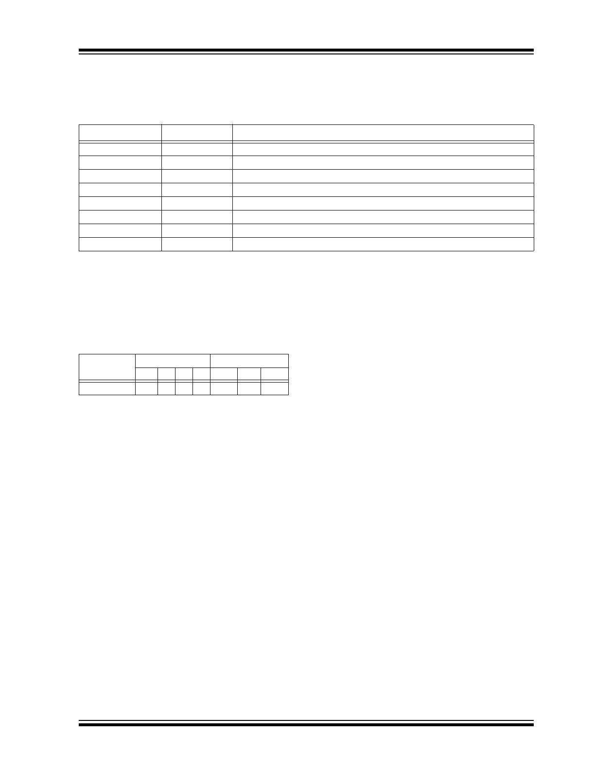
The descriptions of the pins are listed in Table 3-1.
TABLE 3-1:
PIN FUNCTION TABLES
3.1
Slave Address Pins (A0, A1, A2 )
A0, A1 and A2 are device slave address input pins.
The address pins correspond to the Least Significant
bits (LSbs) of the address byte (see Section 5.1.4
“Address Byte”). The Most Significant bits A6, A5, A4,
A3 are factory set. This is shown in Table 3-2.
3.2
Ground Pin (GND)
The GND pin is the system ground pin.
3.3
Open-Drain Serial Data Line (SDA)
SDA is a bidirectional input/output pin, used to serially
transmit data to/from the host controller. This pin
requires a pull-up resistor. (See Section 5.0 “Serial
Communication”).
3.4
Open-Drain Serial Clock Line
(SCLK)
The SCLK is a clock input pin. All communication and
timing is relative to the signal on this pin. The clock is
generated by the host or master controller on the bus.
(See Section 5.0 “Serial Communication”).
3.5
Open-Drain Temperature Event
Output pin (Event)
The MCP9805 Event pin is an open-drain output. The
device outputs a signal when the ambient temperature
goes beyond the user-programmed temperature limit.
(see Section 4.2.3 “Event Output Configuration”).
3.6
Power Pin (V
DD
)
V
DD
is the power pin. The operating voltage range, as
specified in the DC electrical specification table, is
applied on this pin.
DFN/TSSOP
Symbol
Pin Function
1
A0
Slave Address
2
A1
Slave Address
3
A2
Slave Address
4
GND
Ground
5
SDA
Serial Data Line
6
SCLK
Serial Clock Line
7
Event
Temperature Event Output
8
V
DD
Power
TABLE 3-2:
MCP9805 ADDRESS BYTE
Device
Address Code
Slave Address
A6
A5 A4 A3
A2
A1
A0
MCP9805
0
0
1
1
X
X
X
Note:
User-selectable address is shown by X.
MCP9805
DS21977C-page 8
2005-2013 Microchip Technology Inc.
4.0
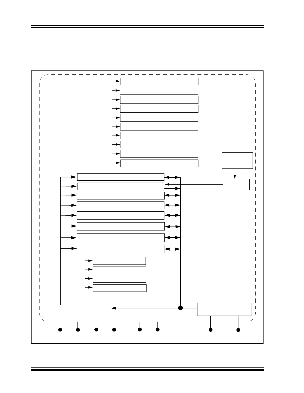
FUNCTIONAL DESCRIPTION
The MCP9805 temperature sensors consist of a band
gap temperature sensor, a Delta-Sigma
Analog-to-Digital Converter (
ADC) and
user-programmable registers using a 2-wire
SMBus/Standard mode I
2
C compatible serial interface
protocol. Figure 4-1 shows a block diagram of the
register structure.
FIGURE 4-1:
Register Structure Block Diagram.
Clear Event Output Interrupt
Temperature Register (T
A
)
Temperature Upper-Boundary (T
UPPER
)
Temperature Lower-Boundary (T
LOWER
)
Configuration Register
ADC
Band Gap
Temperature
Sensor
Event Output Status
Enable/Disable Event Output
Critical Event Output only
Event Output Polarity, Active-High/Low
Critical Temperature Limit (T
CRIT
)
Device Capability Register
Measurement Resolution
Measurement Accuracy
Temperature Event Output
Register Pointer
SMBus/Standard I
2
C™
Interface
Critical Boundary Trip Lock
Event Boundary Window Lock bit
Continuous Conversion or Shutdown
Event Output Hysteresis
Manufacturer Identification Register
Device Identification and Revision Register
Event Output Comparator/Interrupt
Measurement Range
V
DD
GND
SDA
SCLK
A2
Event
A0
A1

2005-2013 Microchip Technology Inc.
DS21977C-page 9
MCP9805
4.1
Registers
The MCP9805 has several registers that are
user-accessible. These registers include the Capability
register, Configuration register, Event Temperature
Upper-Boundary and Lower-Boundary Trip registers,
Critical Temperature Trip register, Temperature regis-
ter, Manufacturer Identification register and Device
Identification register.
The Temperature register is read-only, used to access
the ambient temperature data. The data is loaded in
parallel to this register after t
CONV
. The Event
Temperature Upper-Boundary and Lower-Boundary
Trip registers are read/writes. If the ambient tempera-
ture drifts beyond the user-specified limits, the
MCP9805 outputs a signal using the Event pin (refer to
Section 4.2.3 “Event Output Configuration”). In
addition, the Critical Temperature Trip register is used
to provide an additional critical temperature limit.
The Capability register is used to provide bits
describing the MCP9805’s capability in measurement
resolution, measurement range and device accuracy.
The device Configuration register provides access to
configure the MCP9805’s various features. These
registers are described in further detail in the following
sections.
The registers are accessed by sending a Register
Pointer to the MCP9805 using the serial interface. This
is an 8-bit write-only pointer. However, the three Least
Significant bits (3-LSbs) are used as pointers and all
unused bits (bits 7-3) need to be cleared or set to ‘0’.
Register 4-1 describes the pointer or the address of
each register.
REGISTER 4-1:
REGISTER ADDRESS POINTER (WRITE-ONLY)
W-0
W-0
W-0
W-0
W-0
W-0
W-0
W-0
0
0
0
0
0
P2
P1
P0
bit 7
bit 0
bit 7-3
Writable Bits: Write ‘0’
Bits 7-3 must always be cleared or written to ‘0’. This device has additional registers that are
reserved for test and calibration. If these registers are accessed, the device may not perform
according to the specification.
bit 2-0
Pointer Bits:
000
=
Capability register
001
=
Configuration register (CONFIG)
010
=
Event Temperature Upper-Boundary Trip register (T
UPPER
)
011
=
Event Temperature Lower-Boundary Trip register (T
LOWER
)
100
=
Critical Temperature Trip register (T
CRIT
)
101
=
Temperature register (T
A
)
110
=
Manufacturer ID register
111
=
Device ID/Revision register
Legend:
R = Readable bit
W = Writable bit
U = Unimplemented bit, read as ‘0’
- n = Value at POR
‘1’ = Bit is set
‘0’ = Bit is cleared
x = Bit is unknown
MCP9805
DS21977C-page 10
2005-2013 Microchip Technology Inc.
4.1.1
CAPABILITY REGISTER
This is a read-only register used to identify the temper-
ature sensor capability. In this case, the MCP9805 is
capable of providing temperature at 0.25°C resolution,
measuring temperature below and above 0°C,
providing ±1°C and ±2°C accuracy over the active and
monitor temperature ranges (respectively) and provid-
ing user-programmable temperature event boundary
trip limits. Register 4-2 describes the Capability
register. These functions are described in further detail
in the following sections.
REGISTER 4-2:
CAPABILITY REGISTER (READ-ONLY)
ADDRESS ‘0000 0000’b
bit 15-5
Unimplemented: Read as ‘0’
bit 4-3
RESOLUTION bits:
00
=
0.5 °C/LSb
01
=
0.25 °C/LSb (default resolution)
10
=
0.125 °C/LSb
11
=
0.0625 °C/LSb
bit 2
TEMPERATURE MEASUREMENT RANGE (Meas. Range) bit:
0
= T
A
0x0000 (Hexadecimal) for temperature below 0°C
1
= The part can measure temperature below 0°C
bit 1
ACCURACY bit:
0
= Accuracy
±2°C from +75°C to +95°C (Active Range) and ±3°C from +40°C to +125°C
(Monitor Range)
1
= Accuracy
±1°C from +75°C to +95°C (Active Range) and ±2°C from +40°C to +125°C
(Monitor Range)
bit 0
BASIC CAPABILITY (Temp. Event) bit:
0
= No defined function (This bit will never be cleared or set to ‘0’).
1
= The part has temperature boundary trip limits (T
UPPER
/T
LOWER
/T
CRIT
registers) and a temperautre
event output (JC 42.4 required feature).
Upper-Half:
U-0
U-0
U-0
U-0
U-0
U-0
U-0
U-0
—
—
—
—
—
—
—
—
bit 15
bit 8
Lower-Half:
U-0
U-0
U-0
R-0
R-1
R-1
R-1
R-1
—
Resolution
Meas.
Range
Accuracy
Temp.
Event
bit 7
bit 0
Legend:
R = Readable bit
W = Writable bit
U = Unimplemented bit, read as ‘0’
- n = Value at POR
‘1’ = Bit is set
‘0’ = Bit is cleared
x = Bit is unknown