
2005-2013 Microchip Technology Inc.
DS21937B-page 1
TC4423M/TC4424M/TC4425M
Features
• High Peak Output Current: 3A
• Wide Input Supply Voltage Operating Range:
- 4.5V to 18V
• High Capacitive Load Drive Capability:
- 1800 pF in 25 ns
• Short Delay Times: <40 ns (typ)
• Matched Rise/Fall Times
• Low Supply Current:
- With Logic ‘1’ Input – 3.5 mA (Max)
- With Logic ‘0’ Input – 350 µA (Max)
• Low Output Impedance: 3.5
(typ)
• Latch-Up Protected: Will Withstand 1.5A Reverse
Current
• Logic Input: Will Withstand Negative Swing Up To
5V
• ESD Protected: 4 kV
• Pin-compatible with the TC4426M/TC4427M/
TC4428M and TC4426AM/TC4427AM/
TC4428AM devices
• Wide Operating Temperature Range:
- -55°C to +125°C
• See TC4423/TC4424/TC4425 Data Sheet
(DS21421) for additional temperature range and
packaging offerings
Applications
• Switch-mode Power Supplies
• Pulse Transformer Drive
• Line Drivers
General Description
The TC4423M/TC4424M/TC4425M devices are a
family of 3A, dual output buffers/MOSFET drivers. Pin-
compatible with both the TC4426M/TC4427M/
TC4428M and TC4426AM/4427AM/4428AM families
(dual 1.5A drivers), the TC4423M/TC4424M/TC4425M
family has an increased latch-up current rating of 1.5A,
making them even more robust for operation in harsh
electrical environments.
As MOSFET drivers, the TC4423M/TC4424M/
TC4425M can easily charge 1800 pF gate capacitance
in under 35 nsec, while providing low enough
impedances in both the on and off states to ensure the
MOSFET's intended state will not be affected, even by
large transients.
The TC4423M/TC4424M/TC4425M inputs may be
driven directly from either TTL or CMOS (2.4V to 18V).
In addition, 300 mV of hysteresis is built-in to provide
noise immunity and to allow the device to be driven
from slowly rising or falling waveforms.
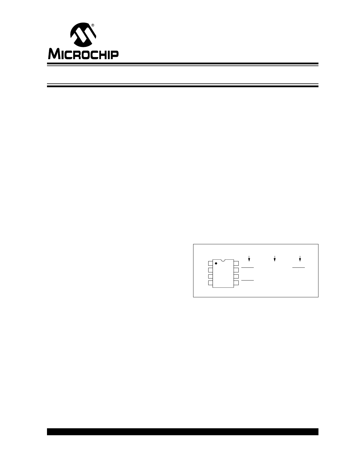
Package Types
8-Pin CERDIP
1
2
3
4
NC
5
6
7
8
OUT A
OUT B
NC
IN A
GND
IN B
V
DD
T
C
4423M
T
C
4424M
TC4423M TC4424M
NC
OUT A
OUT B
V
DD
TC4425M
NC
OUT A
OUT B
V
DD
T
C
4425M
3A Dual High-Speed Power MOSFET Drivers
TC4423M/TC4424M/TC4425M
DS21937B-page 2
2005-2013 Microchip Technology Inc.
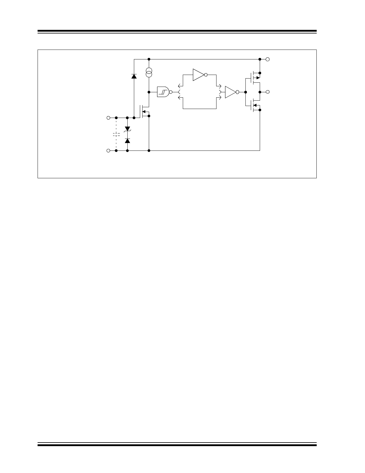
Functional Block Diagram
Effective
Input C = 20 pF
(Each Input)
TC4423M Dual Inverting
TC4424M Dual Non-inverting
TC4425M One Inverting,
Output
Input
GND
(1)
V
DD
300 mV
4.7V
Inverting
Non-inverting
Note 1: Unused inputs should be grounded.
One Non-inverting
2005-2013 Microchip Technology Inc.
DS21937B-page 3
TC4423M/TC4424M/TC4425M
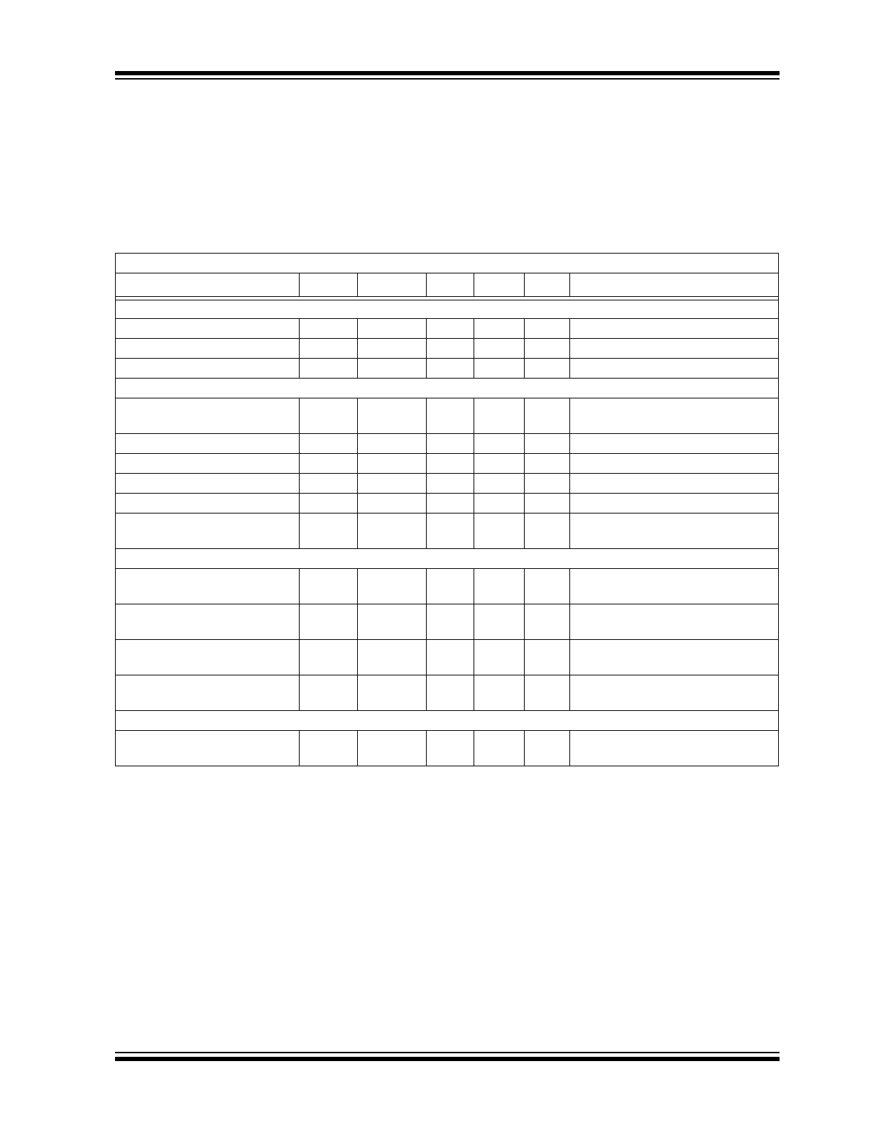
1.0
ELECTRICAL
CHARACTERISTICS
Absolute Maximum Ratings †
Supply Voltage ................................................................+22V
Input Voltage, IN A or IN B .......... (V
DD
+ 0.3V) to (GND – 5V)
† Notice: Stresses above those listed under "Maximum
Ratings" may cause permanent damage to the device. This is
a stress rating only and functional operation of the device at
those or any other conditions above those indicated in the
operational sections of this specification is not intended.
Exposure to maximum rating conditions for extended periods
may affect device reliability.
DC CHARACTERISTICS
Electrical Specifications: Unless otherwise indicated, T
A
= +25°C, with 4.5V
V
DD
18V.
Parameters
Sym
Min
Typ
Max
Units
Conditions
Input
Logic ‘1’, High Input Voltage
V
IH
2.4
—
—
V
Logic ‘0’, Low Input Voltage
V
IL
—
—
0.8
V
Input Current
I
IN
-1
—
1
µA
0V
V
IN
V
DD
Output
High Output Voltage
V
OH
V
DD
–
0.025
—
—
V
Low Output Voltage
V
OL
—
—
0.025
V
Output Resistance, High
R
OH
—
2.8
5
I
OUT
= 10 mA, V
DD
= 18V
Output Resistance, Low
R
OL
—
3.5
5
I
OUT
= 10 mA, V
DD
= 18V
Peak Output Current
I
PK
—
3
—
A
Latch-Up Protection Withstand
Reverse Current
I
REV
—
>1.5
—
A
Duty cycle
2%, t 300 µsec.
Switching Time (Note 1)
Rise Time
t
R
—
23
35
ns
Figure 4-1, Figure 4-2,
C
L
= 1800 pF
Fall Time
t
F
—
25
35
ns
Figure 4-1, Figure 4-2,
C
L
= 1800 pF
Delay Time
t
D1
—
33
75
ns
Figure 4-1, Figure 4-2,
C
L
= 1800 pF
Delay Time
t
D2
—
38
75
ns
Figure 4-1, Figure 4-2,
C
L
= 1800 pF
Power Supply
Power Supply Current
I
S
—
—
1.5
0.15
2.5
0.25
mA
V
IN
= 3V (Both inputs)
V
IN
= 0V (Both inputs)
Note 1:
Switching times ensured by design.
TC4423M/TC4424M/TC4425M
DS21937B-page 4
2005-2013 Microchip Technology Inc.
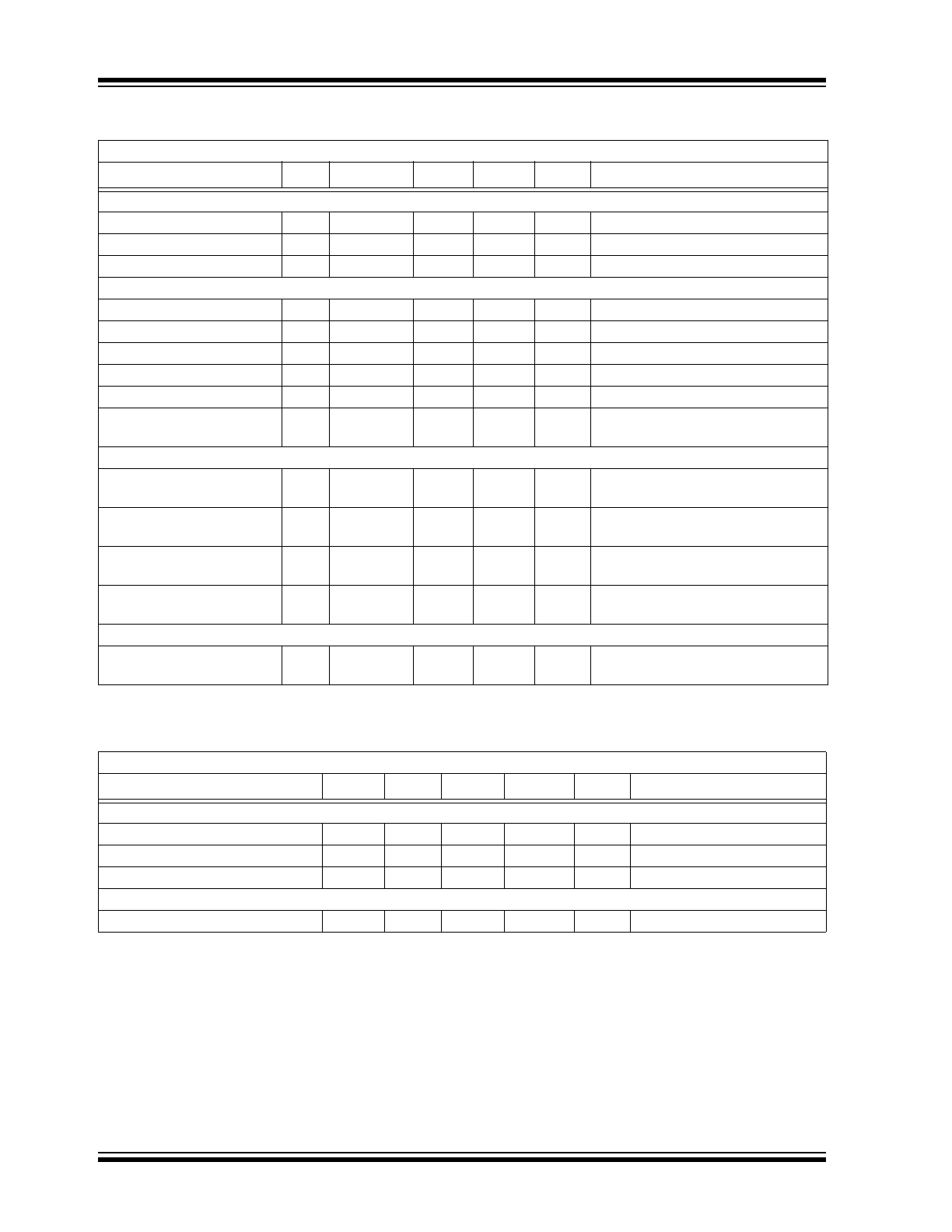
DC CHARACTERISTICS (OVER OPERATING TEMPERATURE RANGE)
TEMPERATURE CHARACTERISTICS
Electrical Specifications: Unless otherwise indicated, operating temperature range with 4.5V
V
DD
18V.
Parameters
Sym
Min
Typ
Max
Units
Conditions
Input
Logic ‘1’, High Input Voltage
V
IH
2.4
—
—
V
Logic ‘0’, Low Input Voltage
V
IL
—
—
0.8
V
Input Current
I
IN
-10
—
+10
µA
0V
V
IN
V
DD
Output
High Output Voltage
V
OH
V
DD
– 0.025
—
—
V
Low Output Voltage
V
OL
—
—
0.025
V
Output Resistance, High
R
OH
—
3.7
8
I
OUT
= 10 mA, V
DD
= 18V
Output Resistance, Low
R
OL
—
4.3
8
I
OUT
= 10 mA, V
DD
= 18V
Peak Output Current
I
PK
—
3.0
—
A
Latch-Up Protection
Withstand Reverse Current
I
REV
—
>1.5
—
A
Duty cycle
2%, t 300 µsec
Switching Time (Note 1)
Rise Time
t
R
—
28
60
ns
Figure 4-1, Figure 4-2,
C
L
= 1800 pF
Fall Time
t
F
—
32
60
ns
Figure 4-1, Figure 4-2,
C
L
= 1800 pF
Delay Time
t
D1
—
32
100
ns
Figure 4-1, Figure 4-2,
C
L
= 1800 pF
Delay Time
t
D2
—
38
100
ns
Figure 4-1, Figure 4-2,
C
L
= 1800 pF
Power Supply
Power Supply Current
I
S
—
—
2.0
0.2
3.5
0.3
mA
V
IN
= 3V (Both inputs)
V
IN
= 0V (Both inputs)
Note 1: Switching times ensured by design.
Electrical Specifications: Unless otherwise noted, all parameters apply with 4.5V
V
DD
18V.
Parameters
Sym
Min
Typ
Max
Units
Conditions
Temperature Ranges
Specified Temperature Range (M)
T
A
-55
—
+125
ºC
Maximum Junction Temperature
T
J
—
—
+150
ºC
Storage Temperature Range
T
A
-65
—
+150
ºC
Package Thermal Resistances
Thermal Resistance, 8L-CERDIP
JA
—
150
—
ºC/W
2005-2013 Microchip Technology Inc.
DS21937B-page 5
TC4423M/TC4424M/TC4425M
2.0
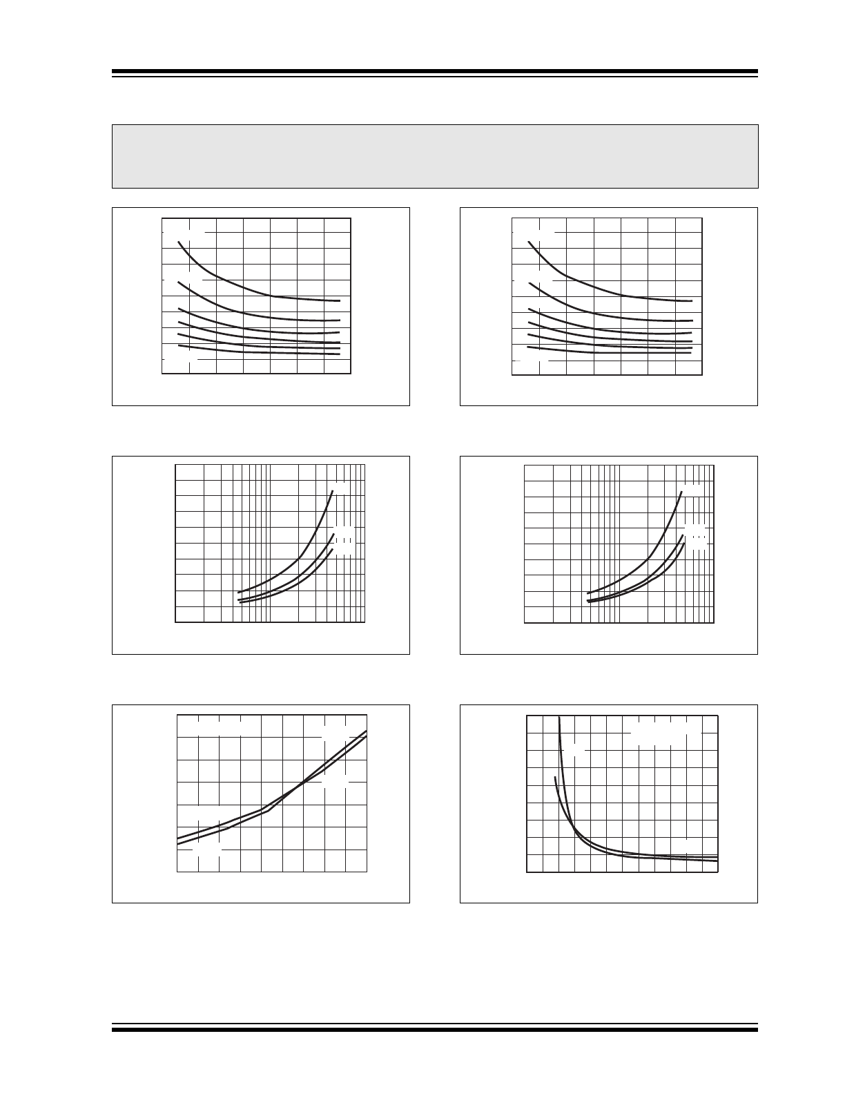
TYPICAL PERFORMANCE CURVES
FIGURE 2-1:
Rise Time vs. Supply
Voltage.
FIGURE 2-2:
Rise Time vs. Capacitive
Load.
FIGURE 2-3:
Rise and Fall Times vs.
Temperature.
FIGURE 2-4:
Fall Time vs. Supply
Voltage.
FIGURE 2-5:
Fall Time vs. Capacitive
Load.
FIGURE 2-6:
Propagation Delay vs. Input
Amplitude.
Note:
The graphs and tables provided following this note are a statistical summary based on a limited number of
samples and are provided for informational purposes only. The performance characteristics listed herein
are not tested or guaranteed. In some graphs or tables, the data presented may be outside the specified
operating range (e.g., outside specified power supply range) and therefore outside the warranted range.
4
6
8
10
12
14
16
18
2200 pF
100
80
60
40
20
0
1000 pF
3300 pF
1500 pF
4700 pF
470 pF
t
RISE
(nsec)
V
DD
(V)
100
1000
10,000
5V
10V
15V
100
80
60
40
20
0
t
RISE
(nsec)
C
LOAD
(pF)
TIME (nsec)
32
30
28
26
24
22
20
18
-55
-35
5
25
45
65
85
105 125
-15
t
FALL
t
RISE
T
A
(°C)
t
FALL
t
RISE
C
LOAD
= 2200 pF
4
6
8
10
12
14
16
18
100
80
60
40
20
0
1000 pF
1500 pF
4700 pF
3300 pF
2200 pF
470 pF
t
FALL
(nsec)
V
DD
(V)
100
1000
10,000
5V
10V
15V
100
80
60
40
20
0
t
FALL
(nsec)
C
LOAD
(pF)
100
80
60
40
20
DELAY TIME (nsec)
INPUT (V)
0
1
2
3
4
5
6
7
8
9
10 11 12
t
D1
t
D2
C
LOAD
= 2200 pF
V
DD
= 10V
TC4423M/TC4424M/TC4425M
DS21937B-page 6
2005-2013 Microchip Technology Inc.
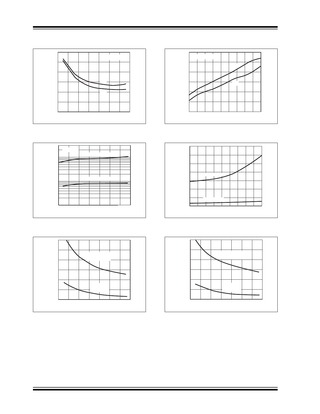
Typical Performance Curves (Continued)
FIGURE 2-7:
Propagation Delay Time vs.
Supply Voltage.
FIGURE 2-8:
Quiescent Current vs.
Supply Voltage.
FIGURE 2-9:
Output Resistance (Output
High) vs. Supply Voltage.
FIGURE 2-10:
Propagation Delay Time vs.
Temperature.
FIGURE 2-11:
Quiescent Current vs.
Temperature.
FIGURE 2-12:
Output Resistance (Output
Low) vs. Supply Voltage.
50
45
40
35
30
25
20
4
6
8
10
12
14
16
18
DELAY TIME (nsec)
V
DD
(V)
C
LOAD
= 2200 pF
t
D1
t
D2
1
0.1
0.01
4
6
8
10
12
14
16
18
BOTH INPUTS = 1
BOTH INPUTS = 0
V
DD
(V)
I
QUIESCENT
(mA)
T
A
= 25°C
14
12
10
8
6
4
2
4
6
8
10
12
14
16
18
TYP @
T
A
= +25
°C
WORST CASE
@ T
J
= +150
°C
V
DD
(V)
R
DS(ON)
(
Ω
)
50
45
40
35
30
25
20
DELAY TIME (nsec)
-55
-35
-15
5
25
45
65
85
105 125
t
D2
t
D1
C
LOAD
= 2200 pF
T
A
(°C)
-55
-35
-15
5
25
45
65
85
105 125
1.4
1.2
1.0
0.8
0.6
0.4
0.2
0.0
BOTH INPUTS = 1
BOTH INPUTS = 0
T
A
(°C)
I
QUIESCENT
(mA)
14
12
10
8
6
4
2
4
6
8
10
12
14
16
18
WORST CASE
@ T
J
= +150
°C
V
DD
(V)
TYP @
T
A
= +25
°C
R
DS(ON)
(
Ω
)
2005-2013 Microchip Technology Inc.
DS21937B-page 7
TC4423M/TC4424M/TC4425M
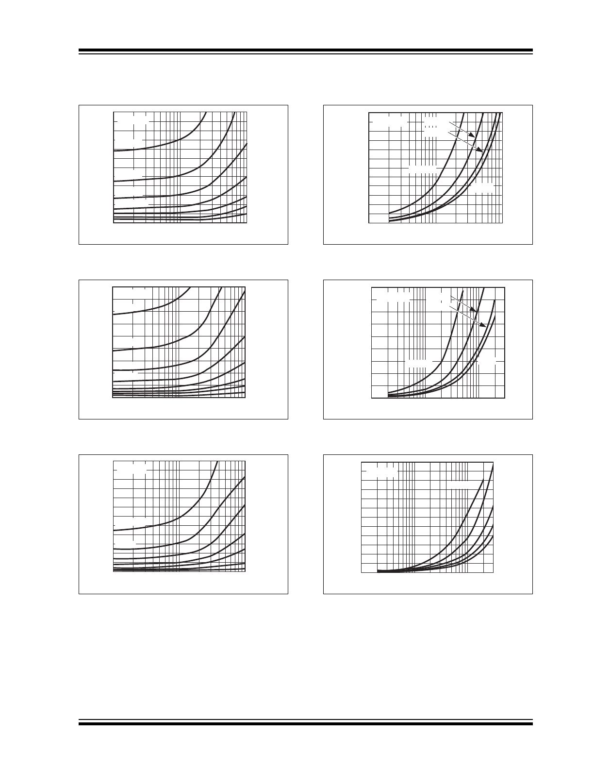
Typical Performance Curves (Continued)
Note: Load on single output only
FIGURE 2-13:
Supply Current vs.
Capacitive Load.
FIGURE 2-14:
Supply Current vs.
Capacitive Load.
FIGURE 2-15:
Supply Current vs.
Capacitive Load.
FIGURE 2-16:
Supply Current vs.
Frequency.
FIGURE 2-17:
Supply Current vs.
Frequency.
FIGURE 2-18:
Supply Current vs.
Frequency.
100
1000
10,000
60
50
40
30
20
10
0
355 kHz
200 kHz
35.5 kHz
634 kHz
CLOAD (pF)
112.5 kHz
20 kHz
63.4 kHz
V
DD
= 18V
I
SUPPLY
(mA)
100
1000
10,000
2 MHz
1.125 MHz
634 kHz
355 kHz
200 kHz
112.5 kHz
63.4 kHz
20 kHz
90
80
70
60
50
40
30
20
10
0
I
SUPPLY
(mA)
CLOAD (pF)
V
DD
= 12V
100
1000
10,000
634 kHz
355 kHz
112.5 kHz
20 kHz
2 MHz
1.125 MHz
3.55 MHz
120
100
80
60
40
20
0
CLOAD (pF)
I
SUPPLY
(mA)
V
DD
= 6V
10,000 pF
FREQUENCY (kHz)
60
50
40
30
20
10
0
10
100
1000
3300 pF
100 pF
1000 pF
I
SUPPLY
(mA)
V
DD
= 18V
10,000 pF
10
100
1000
FREQUENCY (kHz)
90
80
70
60
50
40
30
20
10
0
100 pF
3300 pF
1000 pF
I
SUPPLY
(mA)
V
DD
= 12V
10
100
1000
FREQUENCY (kHz)
1000 pF
4700 pF
100 pF
120
100
80
60
40
20
0
10,000 pF
2200 pF
I
SUPPLY
(mA)
V
DD
= 6V
TC4423M/TC4424M/TC4425M
DS21937B-page 8
2005-2013 Microchip Technology Inc.
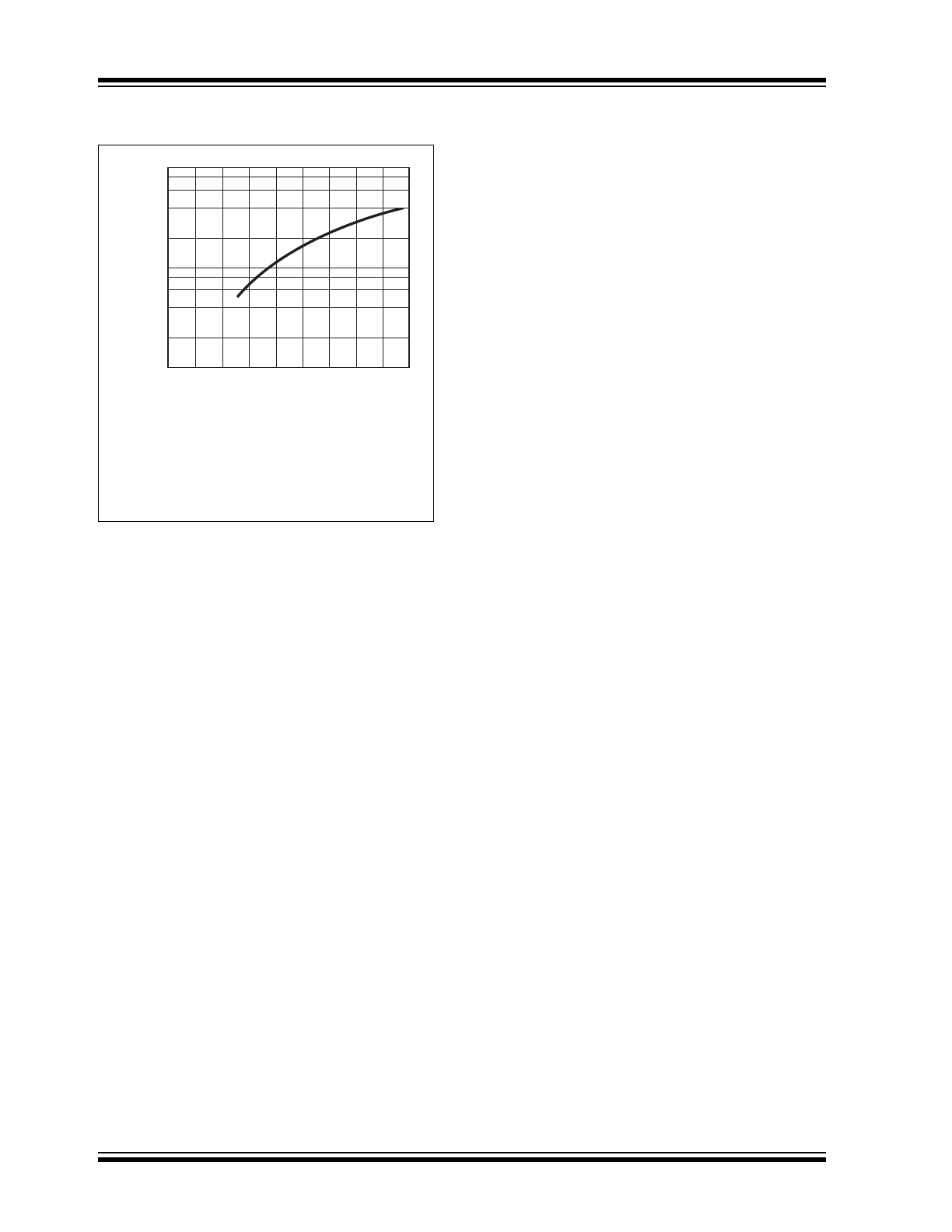
Typical Performance Curves (Continued)
FIGURE 2-19:
TC4423M Crossover
Energy.
10-8
8
10-7
A • sec
0
2
4
6
8
10
12
14
16
18
6
4
2
8
6
4
2
10-9
V
IN
(V)
Note:
The values on this graph represent the
loss seen by both drivers in a package
during one complete cycle. For a single
driver, divide the stated values by 2. For
a single transition of a single driver,
divide the stated value by 4.
2005-2013 Microchip Technology Inc.
DS21937B-page 9
TC4423M/TC4424M/TC4425M
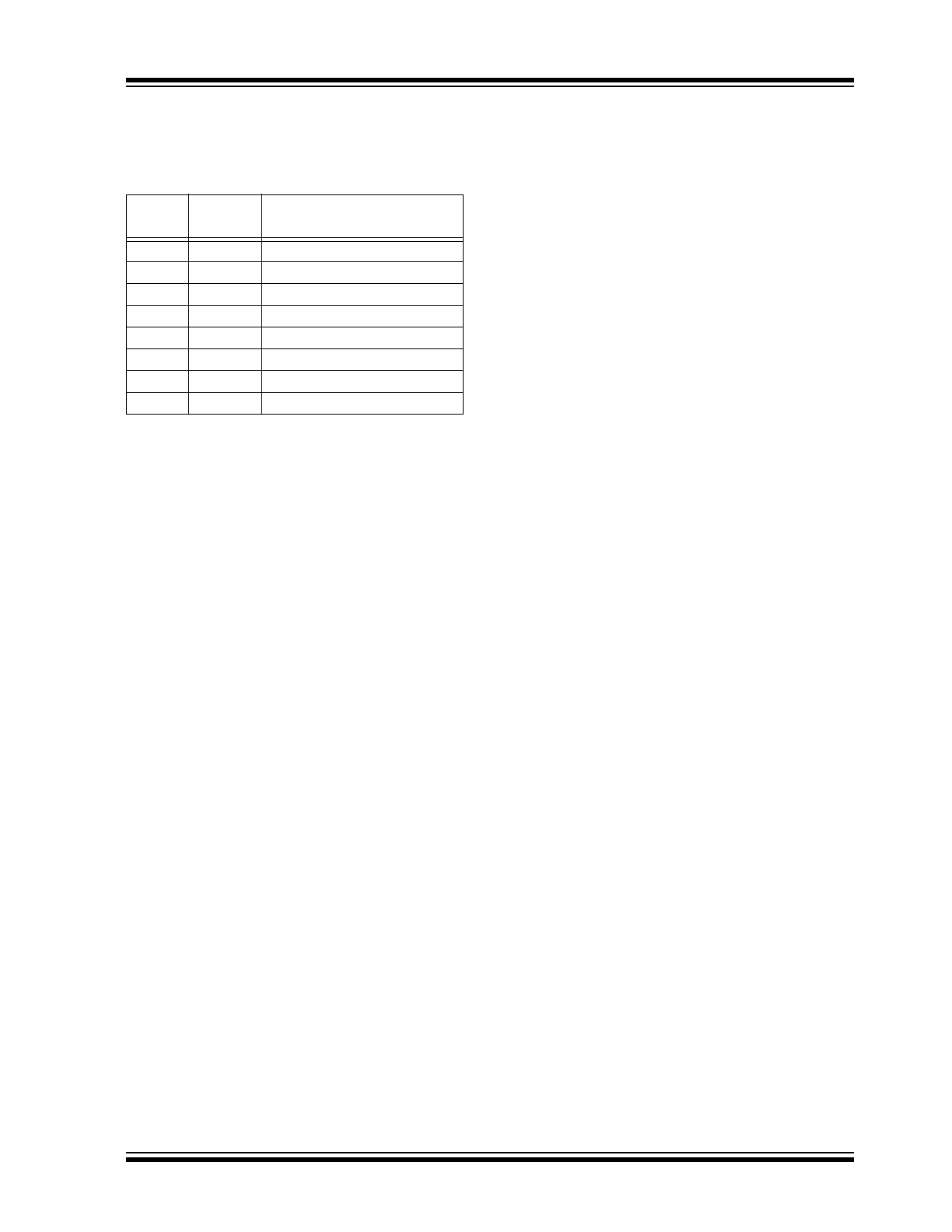
3.0
PIN DESCRIPTIONS
The descriptions of the pins are listed in Table 3-1.
TABLE 3-1:
PIN FUNCTION TABLE
3.1
Input A (IN A)
IN A is a TTL/CMOS-compatible input that controls
OUT A. This input has 300 mV of hysteresis between
the high and low input levels that allows it to be driven
from slow rising and falling signals, as well as providing
noise immunity.
3.2
Input B (IN B)
IN B is a TTL/CMOS-compatible input that controls
OUT B. This input has 300 mV of hysteresis between
the high and low input levels that allows it to be driven
from slow rising and falling signals, as well as providing
noise immunity.
3.3
Output B (OUT B)
OUT B is a CMOS push-pull output that is capable of
sourcing and sinking 3A peaks of current (V
DD
= 18V).
The low output impedance ensures the gate of the
external MOSFET will stay in the intended state even
during large transients. This output also has a reverse
current latch-up rating of 1.5A.
3.4
Output A (OUT A)
OUT A is a CMOS, push-pull output that is capable of
sourcing and sinking 3A peaks of current (V
DD
= 18V).
The low output impedance ensures the gate of the
external MOSFET will stay in the intended state even
during large transients. This output also has a reverse
current latch-up rating of 1.5A.
3.5
Supply Input (V
DD
)
V
DD
is the bias supply input for the MOSFET driver and
has a voltage range of 4.5V to 18V. This input must be
decoupled to ground with a local ceramic capacitor.
This bypass capacitor provides a localized low-
impedance path for the peak currents that are to be
provided to the load.
3.6
Ground (GND)
GND is the device return pin. The ground pin(s) should
have a low-impedance connection to the bias supply
source return. High peak currents will flow out the
ground pin(s) when the capacitive load is being
discharged.
8-Pin
CERDIP
Symbol
Description
1
NC
No connection
2
IN A
Input A
3
GND
Ground
4
IN B
Input B
5
OUT B
Output B
6
V
DD
Supply input
7
OUT A
Output A
8
NC
No connection
TC4423M/TC4424M/TC4425M
DS21937B-page 10
2005-2013 Microchip Technology Inc.
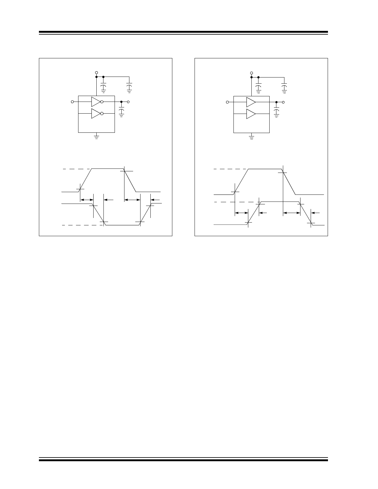
4.0
APPLICATIONS INFORMATION
FIGURE 4-1:
Inverting Driver Switching
Time.
FIGURE 4-2:
Non-inverting Driver
Switching Time.
0.1 µF
+5V
10%
90%
10%
90%
10%
90%
16V
1 µF
WIMA
MKS-2
0V
0V
TC4423M
(1/2 TC4425M)
1
2
C
L
= 1800 pF
Input
Input
Output
t
D1
t
F
t
D2
Input: 100 kHz,
square wave,
Output
t
R
V
DD
= 16V
t
RISE
= t
FALL
10 ns
Ceramic
90%
Input
t
D1
t
F
t
D2
Output
t
R
10%
10%
10%
+5V
16V
0V
0V
90%
90%
Input: 100 kHz,
square wave,
t
RISE
= t
FALL
10 ns
0.1 µF
1 µF
WIMA
MKS-2
TC4424M
(1/2 TC4425M)
1
2
C
L
= 1800 pF
Input
Output
V
DD
= 16V
Ceramic