
2004-2013 Microchip Technology Inc.
DS21921C-page 1
MCP1612
Features
• Fixed Switching Frequency: 1.4 MHz
• Input Operating Voltage Range: 2.7V to 5.5V
• Integrated Buck and Synchronous Switches
• Adjustable-Output Voltage Range: 0.8V to 5.0V
• 100% Duty Cycle Capable for Low Input Voltage
• Continuous Output Current Capability: 1A
• Shutdown Control with I
Q
< 0.01
µ
A (Typ.)
• Integrated Soft-Start Feature
• Integrated Undervoltage Lockout (UVLO)
Protection
• Integrated Overtemperature Protection
• Fast Dynamic Response to Line and Load Steps
• Small, 8-Pin DFN and MSOP Packages
• Operating Temperature Range: -40°C to +85°C
Applications
• Network Interface Cards
• Portable Computers
• Set-Top Boxes
• DSL Modems and Routers
• USB-Powered Devices
• GBIC Modules
• High-Speed Data System Bus Termination
• Medical Instruments
• Cellular/GSM/PHS Phones
• +5V or +3.3V Distributed Voltages
Description
The MCP1612 is a 1A, 1.4 MHz, fully-integrated,
current mode-controlled, synchronous buck regulator.
The MCP1612 is packaged in the 8-pin MSOP and
space-saving, 3x3 DFN packages. The DFN package
also provides a lower thermal resistance package
option for high-power, high ambient temperature
applications. With an input operating range from 2.7V
to 5.5V, the MCP1612 is ideal for applications that are
powered by one single-cell Li-Ion, 2- to 3-cell NiMH,
NiCd or alkaline sources.
The output voltage of the MCP1612 is easily set over
the range of 0.8V to 5.0V by using an external resistor
divider. The external inductor and output capacitor size
are minimized due to an internally-fixed, 1.4 MHz clock
being used to set the switching frequency. The fixed
clock allows for continuous, fixed-frequency PWM
operation over the full load range.
The MCP1612 is designed to provide fast dynamic
response to sudden changes in input voltage and load
current to minimize the necessary amount of external
output capacitance.
The MCP1612 can be used with ceramic, tantalum or
aluminum electrolytic output capacitors. Ceramic
capacitors with values as low as 4.7 µF can be used to
keep the output ripple voltage low. For applications that
require better load step performance, the value of the
output capacitor can be increased to 47 µF.
Additional features integrated into the MCP1612
include shutdown capability, soft-start, UVLO,
overcurrent and overtemperature protection.
Package Types
8-Lead DFN
1
2
3
4
8
7
6
5
V
CC
SHDN
COMP
V
IN
P
GND
L
X
A
GND
FB
1
2
3
4
8
7
6
5
V
CC
SHDN
COMP
V
IN
P
GND
L
X
A
GND
FB
8-Lead MSOP
Single 1A, 1.4 MHz Synchronous Buck Regulator
MCP1612
DS21921C-page 2
2004-2013 Microchip Technology Inc.
Functional Block Diagram
NDRV
PDRV
INSET
Circuit
IN
gm
I
SENSE
P-Channel
+
+
Slope Comp.
V
CC
P
GND
V
CC
A
GND
A
GND
A
1.2V
0.8V
–
+
FB
Comp
Leading-
Edge
Blank
Soft-
Disable
Thermal
Shutdown
SHDN
Disable
Undervoltage
Lockout
V
CC
V
IN
L
X
A
GND
P
GND
1.4 MHz Clock
UVLO
UVLO
Disable
Peak Current
Limit
V
REF
Peak Current
Limit
Disable
V
REF
Start
V
BG
(UVLO)
2004-2013 Microchip Technology Inc.
DS21921C-page 3
MCP1612
Typical Application Circuit
MCP1612 3.3V to 1.2V Synchronous Buck Converter
C
IN
10 µF
Ceramic
V
IN
FB
A
GND
P
GND
L
x
1
10
2
C
BYP
0.1 µF
Ceramic
V
CC
SHDN
3
3.3 V
IN
±10%
4
OFF
ON
1000 pF
25 k
Comp
L = 3.3 µH
100 k
200 k
1.2V V
OUT
@ 1A
5
6
7
8
MCP1612
C
OUT
10 µF
Ceramic
MCP1612
DS21921C-page 4
2004-2013 Microchip Technology Inc.
1.0
ELECTRICAL
CHARACTERISTICS
Absolute Maximum Ratings †
V
IN
– A
GND
.......................................................................6.0V
(SHDN, FB, V
CC
, Comp ........... (A
GND
– 0.3V) to (V
IN
+ 0.3V)
L
X
to P
GND
.............................................. -0.3V to (V
IN
+ 0.3V)
P
GND
to A
GND
................................................... -0.3V to +0.3V
Output Short Circuit Current ................................. Continuous
Storage temperature .....................................-65°C to +150°C
Ambient Temp. with Power Applied.................-40°C to +85°C
Operating Junction Temperature...................-40°C to +125°C
ESD protection on all pins (HBM)
4 kV
ESD protection on all pins (MM)
300V
† Notice: Stresses above those listed under “Maximum
Ratings” may cause permanent damage to the device. This is
a stress rating only and functional operation of the device at
those or any other conditions above those indicated in the
operational listings of this specification is not implied.
Exposure to maximum rating conditions for extended periods
may affect device reliability.
DC CHARACTERISTICS
Electrical Specifications: Unless otherwise noted, V
IN
= V
CC
= V
SHDN
= 3.3V, V
OUT
= 1.8V, C
IN
= C
OUT
= 10 µF, L = 3.3 µH,
I
LOAD
= 100 mA, T
A
= +25°C. Boldface specifications apply over the T
A
range of -40°C to +85°C.
Parameters
Sym
Min
Typ
Max
Units
Conditions
Input Voltage
Input Operating Voltage
V
IN
2.7
—
5.5
V
Input Shutdown Current
I(V
IN
)
—
0.01
1
µA
Shutdown mode (SHDN = GND)
Input Quiescent Current
I(V
IN
)
—
5
7
mA
I
LOAD
= 0 mA
Oscillator Characteristics
Internal Oscillator Frequency
F
OSC
1.2
1.4
1.6
MHz
Internal Power Swicthes
R
DSon
P-Channel
R
DSon-P
—
300
—
m
I
P
= 250 mA
R
DSon
N-Channel
R
DSon-N
—
300
—
m
I
N
= 250 mA
L
X
Pin Leakage Current
I
LX
-1
—
1
µA
SHDN = 0V, V
IN
= 5.5V, L
X
= 0V,
L
X
= 5.5V
Positive Current Limit Threshold
+I
LX(MAX)
—
2.3
—
A
Negative Current Limit Threshold
-I
LX(MAX)
—
-1.4
—
A
Feedback Characteristics
Transconductance from FB to
COMP
g
m
35
62
90
µA/V
Output Voltage
Output Voltage Range
V
OUT
0.8
—
V
IN
V
Reference Feedback Voltage
V
FB
0.78
0.8
0.82
V
Feedback Input Bias Current
I
VFB
—
1
—
nA
Line Regulation
V
LINE-REG
—
0.15
0.5
%/V
V
IN
= 2.7V to 5.5V, I
LOAD
= 100 mA
Load Regulation
V
LOAD-REG
—
0.25
—
%
V
IN
= 4.2V, I
LOAD
= 100 mA to 1A
Note
1:
The integrated MOSFET switches have an integral diode from the L
X
pin to V
IN
and from L
X
to P
GND
. In cases where
these diodes are forward-biased, the package power dissipation limits must be adhered to. Thermal protection is not
able to regulate the junction temperature for these cases.
2:
UVLO is specified for a falling V
IN
. Once the UVLO is activated, the UVLO-
HYS
must be overcome before the device will
return to operation.
2004-2013 Microchip Technology Inc.
DS21921C-page 5
MCP1612
TEMPERATURE SPECIFICATIONS
Protection Features
Undervoltage Lockout
UVLO
2.4
2.55
2.7
V
Note 2
Undervoltage Lockout Hysteresis
UVLO-
HYS
—
200
—
mV
Thermal Shutdown
T
SHD
—
160
—
°C
Note 1
Thermal Shutdown Hysteresis
T
SHD-HYS
—
9
—
°C
Interface Signal (SHDN)
Logic-High Input
V
IN-HIGH
45
—
—
% of V
IN
Logic-Low Input
V
IN-LOW
—
—
15
% of V
IN
Electrical Specifications: V
IN
= 3.0V to 5.5V, F
OSC
= 1 MHz with 10% Duty Cycle, C
IN
= 0.1 µF. T
A
= -40°C to +125°C.
Parameters
Sym
Min
Typ
Max
Units
Conditions
Temperature Ranges
Storage Temperature Range
T
A
-65
—
+150
°C
Continuous
Maximum Junction Temperature
T
J
—
—
+150
°C
Transient Only
Operating Junction Temperature Range
T
A
- 40
—
+ 125
°C
Continuous Operation
Thermal Package Resistances
Thermal Resistance, 8L-MSOP
JA
—
208
—
°C/W
Typical 4-layer board interconnecting
vias
Thermal Resistance, 8L-DFN
JA
—
41
—
°C/W
Typical 4-layer board interconnecting
vias
DC CHARACTERISTICS (CONTINUED)
Electrical Specifications: Unless otherwise noted, V
IN
= V
CC
= V
SHDN
= 3.3V, V
OUT
= 1.8V, C
IN
= C
OUT
= 10 µF, L = 3.3 µH,
I
LOAD
= 100 mA, T
A
= +25°C. Boldface specifications apply over the T
A
range of -40°C to +85°C.
Parameters
Sym
Min
Typ
Max
Units
Conditions
Note
1:
The integrated MOSFET switches have an integral diode from the L
X
pin to V
IN
and from L
X
to P
GND
. In cases where
these diodes are forward-biased, the package power dissipation limits must be adhered to. Thermal protection is not
able to regulate the junction temperature for these cases.
2:
UVLO is specified for a falling V
IN
. Once the UVLO is activated, the UVLO-
HYS
must be overcome before the device will
return to operation.
MCP1612
DS21921C-page 6
2004-2013 Microchip Technology Inc.
2.0
TYPICAL PERFORMANCE CURVES
Note: Unless otherwise indicated, V
IN
= V
CC
= V
SHDN
= 3.3V, C
OUT
= C
IN
= 10 µF, L = 3.3 µH, I
LOAD
= 100 mA,
T
A
= +25°C. Boldface specifications apply over the T
A
range of -40°C to +85°C.
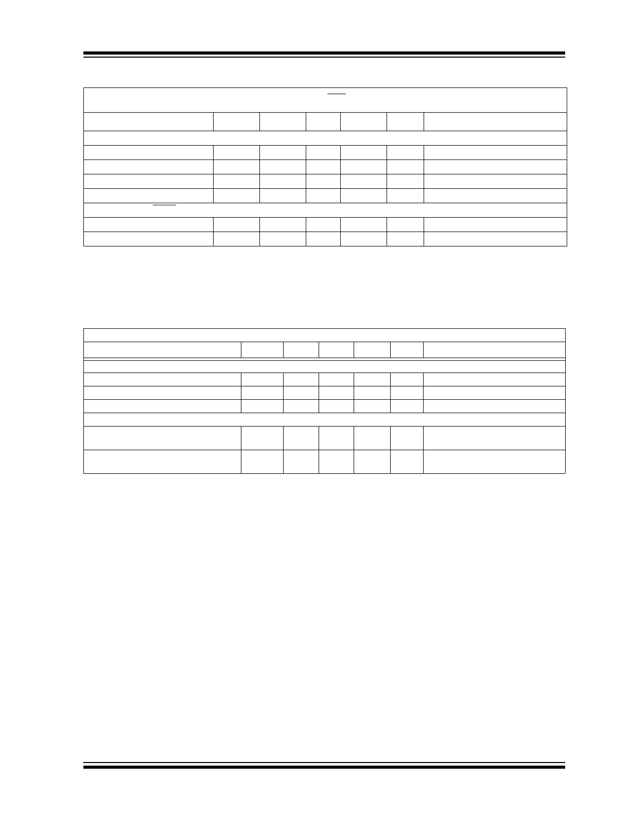
FIGURE 2-1:
Efficiency vs. Load Current,
V
IN
= 3.3V.
FIGURE 2-2:
Efficiency vs. Load Current,
V
IN
= 5.0V.
FIGURE 2-3:
Output Voltage vs.
Load Current.
FIGURE 2-4:
Dropout Voltage vs.
Load Current.
FIGURE 2-5:
Input Quiescent Current vs.
Input Voltage.
FIGURE 2-6:
Oscillator Frequency vs.
Input Voltage.
Note:
The graphs and tables provided following this note are a statistical summary based on a limited number of
samples and are provided for informational purposes only. The performance characteristics listed herein
are not tested or guaranteed. In some graphs or tables, the data presented may be outside the specified
operating range (e.g., outside specified power supply range) and therefore outside the warranted range.
0
10
20
30
40
50
60
70
80
90
100
10
100
1000
Load Current (mA)
E
ffi
cien
cy (
%
)
V
IN
= 3.3V
V
OUT
= 1.2V
V
OUT
= 2.5V
V
OUT
= 1.8V
0
10
20
30
40
50
60
70
80
90
100
10
100
1000
Load Current (mA)
E
ff
icie
n
cy (%
)
V
IN
= 5.0V
V
OUT
= 3.3V
V
OUT
= 2.5V
-1.4
-1.2
-1
-0.8
-0.6
-0.4
-0.2
0
0
200
400
600
800
1000
Load Current (mA)
C
h
an
ge I
n
O
u
tp
ut
Vo
lt
ag
e (
m
V)
V
OUT
= 3.3V, V
IN
= 5.0V
V
OUT
= 1.8V, V
IN
= 3.3V
V
OUT
= 1.2V V
IN
= 3.3V
0.00
0.10
0.20
0.30
0.40
0.50
0
200
400
600
800
1000
Load Current (mA)
D
rop
ou
t V
o
lt
a
g
e
(V
)
V
OUT
= 2.7V
V
OUT
= 3.3V
3.5
4.0
4.5
5.0
5.5
6.0
6.5
2.5
3
3.5
4
4.5
5
5.5
Input Voltage (V)
Inpu
t Qu
iescen
t C
u
rr
en
t (
m
A
)
V
OUT
= 1.8V
T
A
= -40
o
C
T
A
= +25
o
C
T
A
= +85
o
C
1.36
1.37
1.38
1.39
1.40
1.41
1.42
2.5
3
3.5
4
4.5
5
5.5
Input Voltage (V)
Os
cillat
o
r Fr
equen
cy (M
H
z
)
T
A
= -40
o
C
T
A
= +25
o
C
T
A
= +85
o
C
2004-2013 Microchip Technology Inc.
DS21921C-page 7
MCP1612
TYPICAL PERFORMANCE CURVES
(Continued)
Note: Unless otherwise indicated, V
IN
= V
CC
= V
SHDN
= 3.3V, C
OUT
= C
IN
= 10 µF, L = 3.3 µH, I
LOAD
= 100 mA,
T
A
= +25°C. Boldface specifications apply over the T
A
range of -40°C to +85°C.
FIGURE 2-7:
Power-Up from V
IN
.
FIGURE 2-8:
Power-Up from Shutdown.
FIGURE 2-9:
Load Transient Response.
FIGURE 2-10:
Load Transient Response.
FIGURE 2-11:
Line Transient Response.
FIGURE 2-12:
Line Transient Response.
V
IN
2.0V/DIV
V
OUT
1.0V/DIV
Start-up from V
IN
= 0V to 3.3V
1.0 ms/DIV
V
OUT
= 1.8V
SHDN
2.0V/DIV
V
OUT
1.0V/DIV
Start-up from SHDN
1.0 ms/DIV
V
OUT
= 1.8V
V
OUT
200 mV/DIV
I
OUT
500 mA/DIV
I
OUT
= 100 mA to 800 mA
50 µs/DIV
V
OUT
= 1.8V
V
OUT
100 mV/DIV
I
OUT
500 mA/DIV
I
OUT
= 100 mA to 800 mA
500 µs/DIV
V
IN
= 5.0V
V
OUT
= 3.3V
V
IN
2.0V/DIV
V
OUT
50 mV/DIV
Line Step Response, V
IN
= 3.0V to 4.0V
200 µs/DIV
V
OUT
= 1.8V
I
OUT
= 800 mA
V
IN
2.0V/DIV
V
OUT
50 mV/DIV
Line Step Response, V
IN
= 4.5V to 5.5V
200 µs/DIV
V
OUT
= 3.3V
I
OUT
= 800 mA
MCP1612
DS21921C-page 8
2004-2013 Microchip Technology Inc.
TYPICAL PERFORMANCE CURVES
(Continued)
Note: Unless otherwise indicated, V
IN
= V
CC
= V
SHDN
= 3.3V, C
OUT
= C
IN
= 10 µF, L = 3.3 µH, I
LOAD
= 100 mA,
T
A
= +25°C. Boldface specifications apply over the T
A
range of -40°C to +85°C.
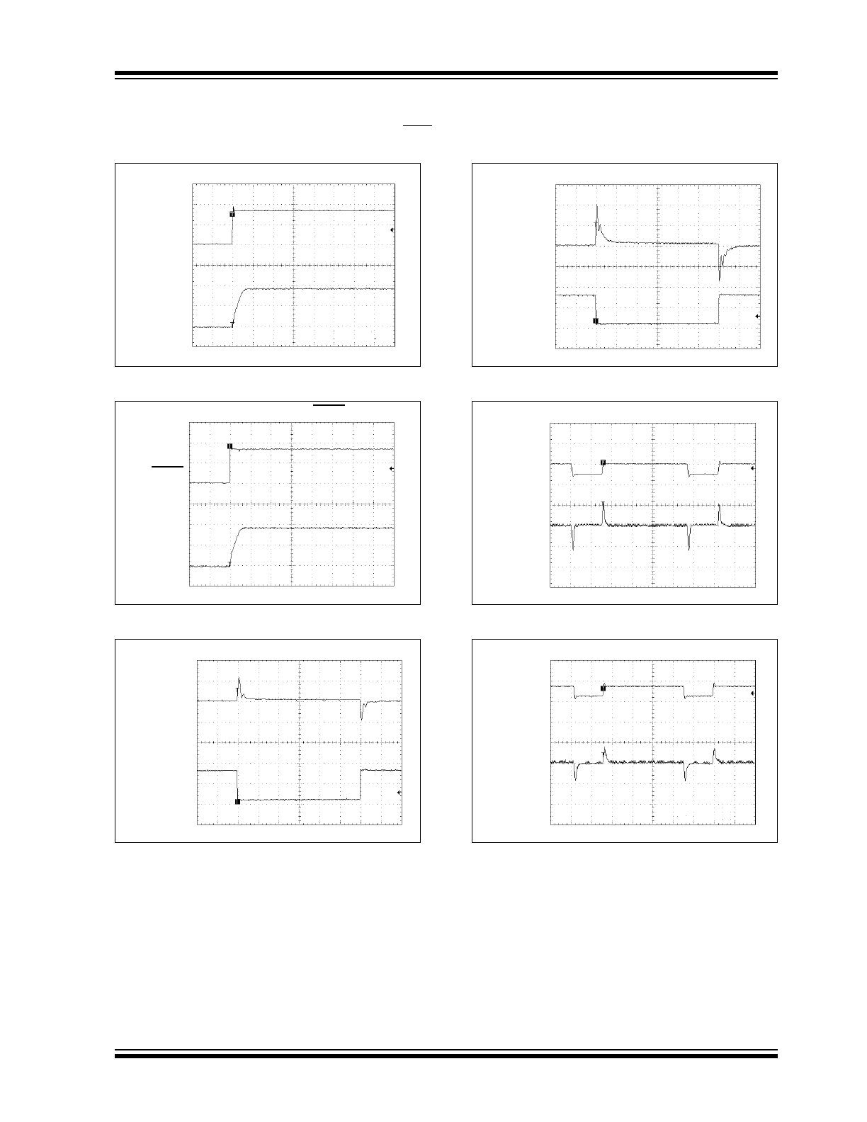
FIGURE 2-13:
Low Load Current Switching
Waveform.
FIGURE 2-14:
High Load Current Switching
Waveform.
L
X
2.0V/DIV
I
IND
100 mA/DIV
500 ns/DIV
V
IN
= 3.3V
V
OUT
10 mV/DIV
I
OUT
= 10 mA, V
OUT
= 1.8V
L
X
5.0V/DIV
I
IND
500 mA/DIV
500 ns/DIV
V
IN
= 3.3V
V
OUT
10 mV/DIV
I
OUT
= 1A, V
OUT
= 1.8V
2004-2013 Microchip Technology Inc.
DS21921C-page 9
MCP1612
3.0
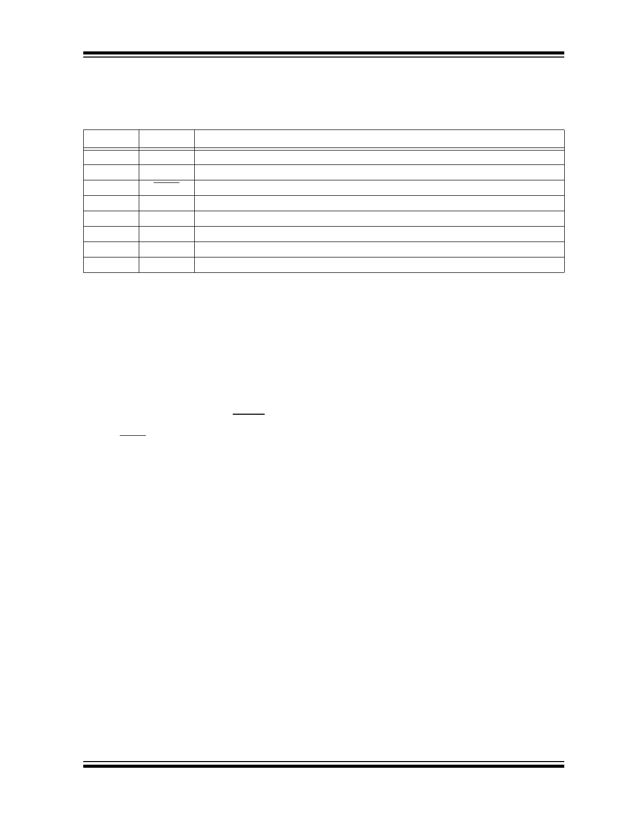
MCP1612 PIN DESCRIPTIONS
The descriptions of the pins are listed in Table 3-1.
TABLE 3-1:
PIN FUNCTION TABLE
3.1
Input Voltage Pin (V
IN
)
Connect the input voltage source to V
IN
. For normal
operation, the voltage on V
IN
should be between +2.7V
and +5.5V. A 10 µF bypass capacitor should be
connected between V
IN
and P
GND
.
3.2
Analog Input Voltage Pin (V
CC
)
V
CC
provides bias for internal analog functions. This
voltage is derived by filtering the V
IN
supply.
3.3
Shutdown Input Pin (SHDN)
Connect SHDN to a logic-level input in order to turn the
regulator on or off. A logic-high (>45% of V
IN
) will
enable the regulator. A logic-low (<15% of V
IN
) will
force the regulator into Shutdown mode. When in
shutdown, both the P-channel and N-channel switches
are turned off.
3.4
Compensation Pin (COMP)
COMP is the internal transconductance amplifier
output pin. External compensation is connected to
COMP for control-loop stabilization.
3.5
Feedback Pin (FB)
Connect the output voltage of the buck converter
through an external resistor divider to FB to regulate
the output voltage. The nominal voltage compared to
this input for pulse termination is 0.8V.
3.6
Analog Ground Pin (A
GND
)
Tie all small-signal ground returns to A
GND
. Noise on
A
GND
can effect the sensitive internal analog
measurements.
3.7
Power Ground Pin (P
GND
)
Connect all large-signal ground returns to P
GND
. These
large-signal traces should have a small loop area and
length to prevent coupling of switching noise to
sensitive traces.
3.8
Buck Inductor Output Pin (L
X
)
Connect L
X
directly to the buck inductor. This pin
carries large signal-level currents; all connections
should be made as short as possible.
Pin No.
Name
Function
1
V
IN
Input Voltage Pin
2
V
CC
Analog Input Voltage Pin
3
SHDN
Shutdown Control Input Pin
4
COMP
Transconductance Amplifier Output Pin
5
FB
Feedback Input Pin
6
A
GND
Analog Ground Pin
7
P
GND
Power Ground Pin
8
L
X
Buck Inductor Output Pin

MCP1612
DS21921C-page 10
2004-2013 Microchip Technology Inc.
4.0
DETAILED DESCRIPTION
4.1
Device Overview
The MCP1612 is a 1A synchronous buck converter
switching at 1.4 MHz to minimize external component
size and cost. While utilizing a fixed-frequency Current
mode architecture, the MCP1612 provides fast
response to sudden load changes, as well as
overcurrent protection in the event of a shorted load.
The input voltage range is 2.7V to 5.5V, while the
output voltage is adjustable by properly setting an
external resistor divider and can range from 0.8V to
V
IN
. Integrated soft-start, UVLO and overtemperature
protection minimize external circuitry and component
count.
4.2
Current Mode Control Scheme
The MCP1612 incorporates a Peak Current mode
control scheme. Peak Current mode is used to obtain
high gain in the PWM control loop for very fast
response to dynamic line and load conditions. With
both the P-channel and N-channel MOSFETs turned
off, the beginning of a cycle occurs on the negative
edge of the internal 1.4 MHz oscillator, the P-channel
MOSFET turns on and current ramps up into the buck
inductor. The inductor current is sensed and tied to one
input of a high-speed comparator. The other input of
the high-speed comparator is the error amplifier output.
This is the amplified difference between the internal
0.8V reference and the divided-down V
OUT
signal at
the FB pin of the MCP1612. When the sensed inductor
current ramps up to the point that is equal to the
amplified error signal, the high-speed comparator
output switches states and the P-channel MOSFET is
turned off until the beginning of the next clock cycle and
the N-channel is turned on. The width of the pulse (or
duty cycle) is ideally determined by the V
OUT
/V
IN
ratio
of the DC/DC converter. The actual duty cycle is slightly
larger to account for the non-ideal losses of the
integrated MOSFET switches and the losses in the
external inductor.
4.3
Low-Dropout Operation
The MCP1612 is capable of operating over a wide
range of input voltages. The PWM architecture allows
for the P-channel MOSFET to achieve 100% duty cycle
operation for applications that have minimal input volt-
age headroom. During 100% Duty Cycle mode, the
output voltage (V
OUT
) is equal to the Output Current
(I
OUT
) x Resistance (P-channel R
DSON
+ R
INDUCTOR
).
4.4
Current Limit
Cycle-by-cycle current limit is used to protect the
MCP1612 from being damaged when an external short
circuit is applied. The typical peak current limit is 2.3A.
If the sensed inductor current reaches the 2.3A limit,
the P-channel MOSFET is turned off, even if the output
voltage is not in regulation.
4.5
Soft-Start
During normal power-up, as V
IN
rises above the UVLO
protection setting (or, in the case of a logic-low to logic-
high transition on the shutdown pin), the rise time of the
MCP1612 output voltage is controlled by the soft-start
feature. This is accomplished by allowing the output of
the error amplifier to slowly rise. This feature prevents
the output voltage from overshooting the desired value
and the sudden inrush of current, depleting the input
capacitors and causing a large dip in input voltage. This
large dip in the input voltage can trip the UVLO thresh-
old, causing the converter to shut down prior to reach-
ing steady-state operation.
4.6
Undervoltage Lockout (UVLO)
The UVLO feature uses a comparator to sense the
input voltage level (V
IN
). If the input voltage is lower
than the voltage necessary to properly operate the
MCP1612, the UVLO feature will hold the converter off.
When V
IN
rises above the necessary input voltage, the
UVLO is released and soft-start begins. For the
MCP1612, the UVLO protection threshold is at a
maximum of 2.7V. Hysteresis is built into the UVLO
circuit to compensate for input impedance. For
example, if there is any resistance between the input
voltage source and the converter (once it starts), there
will be a voltage drop at the converter input equal to
I
IN
x R
IN
. The typical hysteresis for the MCP1612 is
200 mV.
4.7
Overtemperature Protection
The MCP1612 has an integrated overtemperature
protection circuit that monitors the device junction
temperature and shuts the device off if the junction
temperature exceeds the typical 160°C threshold. If the
overtemperature threshold is reached, the soft-start is
reset so that, when the junction temperature cools to
approximately 151°C, the device will automatically
restart and the output voltage will not overshoot.
4.8
Shutdown Input Operation
The SHDN pin is used to turn the MCP1612 on and off.
When the SHDN pin is tied low, the MCP1612 is off.
When tied high, the MCP1612 will be enabled and
begin operation as long as the input voltage is not
below the UVLO threshold.