

2004-2013 Microchip Technology Inc.
DS21896C-page 1
MCP1630/MCP1630V
Features
• High-Speed PWM Operation (12 ns Current
Sense to Output Delay)
• Operating Temperature Range:
- -40°C to +125°C
• Precise Peak Current Limit (±5%) (MCP1630)
• Voltage Mode and Average Current Mode Control
(MCP1630V)
• CMOS Output Driver (drives MOSFET driver or
low-side N-channel MOSFET directly)
• External Oscillator Input
(from PIC
®
Microcontroller (MCU))
• External Voltage Reference Input (for adjustable
voltage or current output application)
• Peak Current Mode Operation > 1 MHz
• Low Operating Current: 2.8 mA (typ.)
• Fast Output Rise and Fall Times: 5.9 ns and
6.2 ns
• Undervoltage Lockout (UVLO) Protection
• Output Short Circuit Protection
• Overtemperature Protection
Applications
• Intelligent Power Systems
• Smart Battery Charger Applications
• Multiple Output/Multiple Phase Converters
• Output Voltage Calibration
• AC Power Factor Correction
• VID Capability (programmed and calibrated by
PIC
®
microcontroller)
• Buck/Boost/Buck-Boost/SEPIC/Flyback/Isolated
Converters
• Parallel Power Supplies
Related Literature
• “MCP1630 NiMH Demo Board User’s Guide”,
Microchip Technology Inc., DS51505, 2004
• “MCP1630 Low-Cost Li-Ion Battery Charger
User’s Guide”, Microchip Technology Inc.,
DS51555, 2005
• “MCP1630 Li-Ion Multi-Bay Battery Charger
User’s Guide”, Microchip Technology Inc.,
DS51515, 2005
• “MCP1630 Dual Buck Demo Board User’s Guide”,
Microchip Technology Inc., DS51531, 2005
Description
The MCP1630/V is a high-speed Pulse Width Modula-
tor (PWM) used to develop intelligent power systems.
When used with a microcontroller unit (MCU), the
MCP1630/V will control the power system duty cycle to
provide output voltage or current regulation. The MCU
can be used to adjust output voltage or current, switch-
ing frequency, maximum duty cycle and other features
that make the power system more intelligent.
Typical applications include smart battery chargers,
intelligent power systems, brick dc/dc converters, ac
power-factor correction, multiple output power supplies,
multi-phase power supplies and more.
The MCP1630/V inputs were developed to be easily
attached to the I/O of a MCU. The MCU supplies the
oscillator and reference to the MCP1630/V to provide
the most flexible and adaptable power system. The
power system switching frequency and maximum duty
cycle are set using the I/O of the MCU. The reference
input can be external, a D/A Converter (DAC) output or
as simple as an I/O output from the MCU. This enables
the power system to adapt to many external signals
and variables in order to optimize performance and
facilitate calibration.
When operating in Current mode, a precise limit is set
on the peak current. With the fast comparator speed
(typically 12 ns), the MCP1630 is capable of providing a
tight limit on the maximum switch current over a wide
input voltage range when compared to other high-speed
PWM controllers.
For Voltage mode or Average Current mode
applications, the MCP1630V provides a larger range for
the external ramp voltage.
Additional protection features include: UVLO,
overtemperature and overcurrent.
Package Type
8-Lead DFN
1
2
3
4
8
7
6
5
FB
CS
OSC IN
COMP
V
IN
V
REF
V
EXT
GND
1
2
3
4
8
7
6
5
FB
CS
OSC IN
COMP
V
IN
V
REF
V
EXT
GND
8-Lead MSOP
(2 mm x 3 mm)
High-Speed, Microcontroller-Adaptable,
Pulse Width Modulator
MCP1630/MCP1630V
DS21896C-page 2
2004-2013 Microchip Technology Inc.
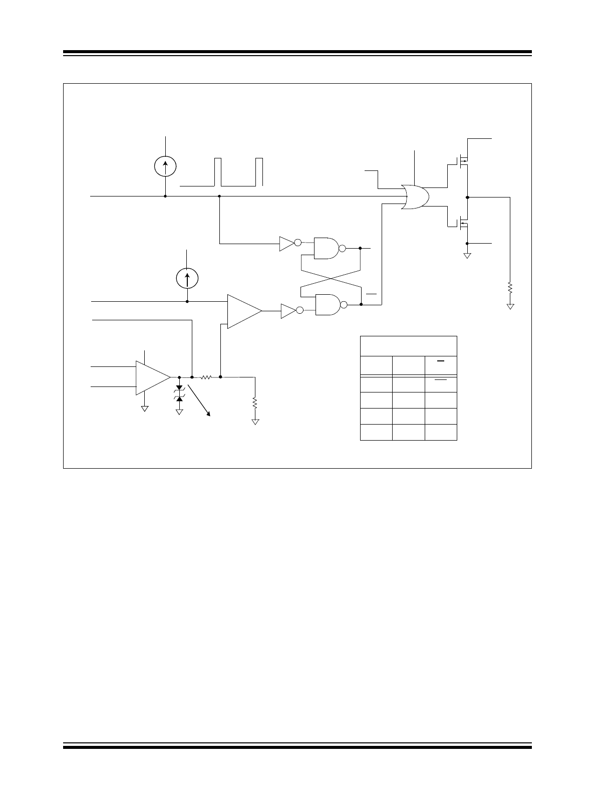
Functional Block Diagram – MCP1630
MCP1630 High-Speed PWM
R
S
Q
Q
EA
+
–
V
REF
FB
Comp
+
–
CS
OSC IN
V
IN
COMP
GND
V
EXT
2R
R
V
IN
2.7V Clamp
Overtemperature
UVLO
100 k
0.1 µA
0.1 µA
V
IN
V
IN
Latch Truth Table
S
R
Q
0
0
Qn
0
1
1
1
0
0
1
1
1
Note:
During overtemperature, V
EXT
driver is high-impedance.
Note
2004-2013 Microchip Technology Inc.
DS21896C-page 3
MCP1630/MCP1630V
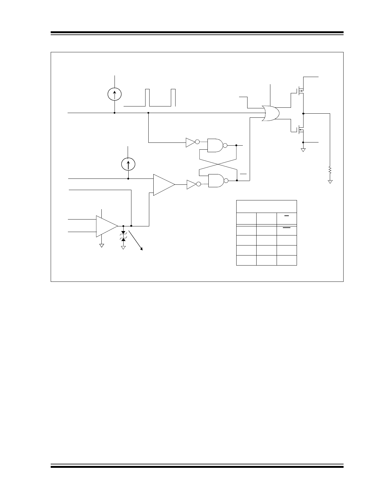
Functional Block Diagram – MCP1630V
MCP1630V High-Speed PWM
R
S
Q
Q
EA
+
–
V
REF
FB
Comp
+
–
CS
OSC IN
V
IN
COMP
GND
V
EXT
V
IN
2.7V Clamp
Overtemperature
UVLO
100 k
0.1 µA
0.1 µA
V
IN
V
IN
Latch Truth Table
S
R
Q
0
0
Qn
0
1
1
1
0
0
1
1
1
Note:
During overtemperature, V
EXT
driver is high-impedance.
Note
MCP1630/MCP1630V
DS21896C-page 4
2004-2013 Microchip Technology Inc.
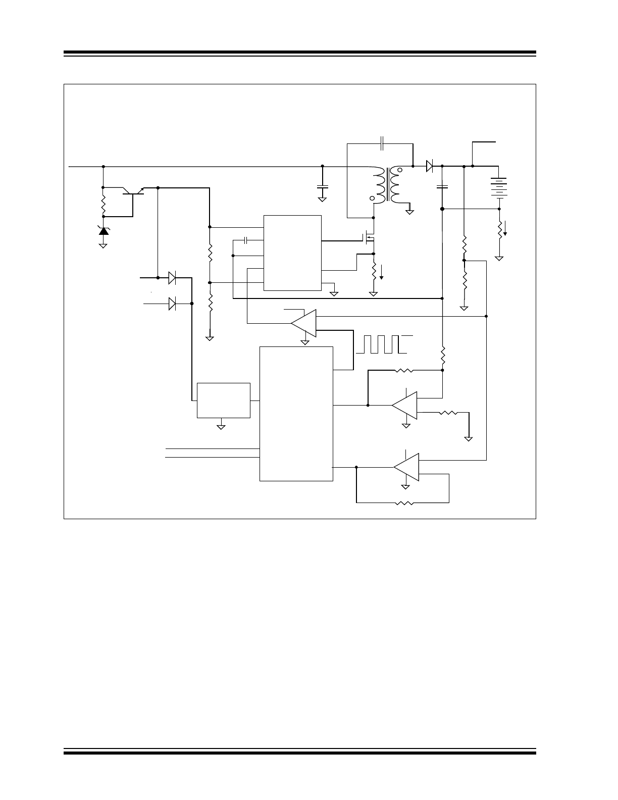
Typical Application Circuit – MCP1630
+V
BATT
MCP1630
+5V Bias
PIC16LF818
1/2 MCP6042
+8V to +15V Input Voltage
MCP1630 NiMH Battery Charger and Fuel Gauge Application Diagram
4 NiMH Cells
N-channel
1:1
SEPIC Converter
Cin
C
OUT
A/D
PWM OUT
A/D
V
DD
I
2
C™ To System
+V
BATT
I
BATT
I
SW
5.7V
+
V
DD
C
C
+
+5V Bias
3V
0V
1/2 MCP6042
V
DD
+
MOSFET
MCP1700
3.0V
SOT23
GND
CS
V
EXT
V
IN
COMP
FB
OSC IN
V
REF
2004-2013 Microchip Technology Inc.
DS21896C-page 5
MCP1630/MCP1630V
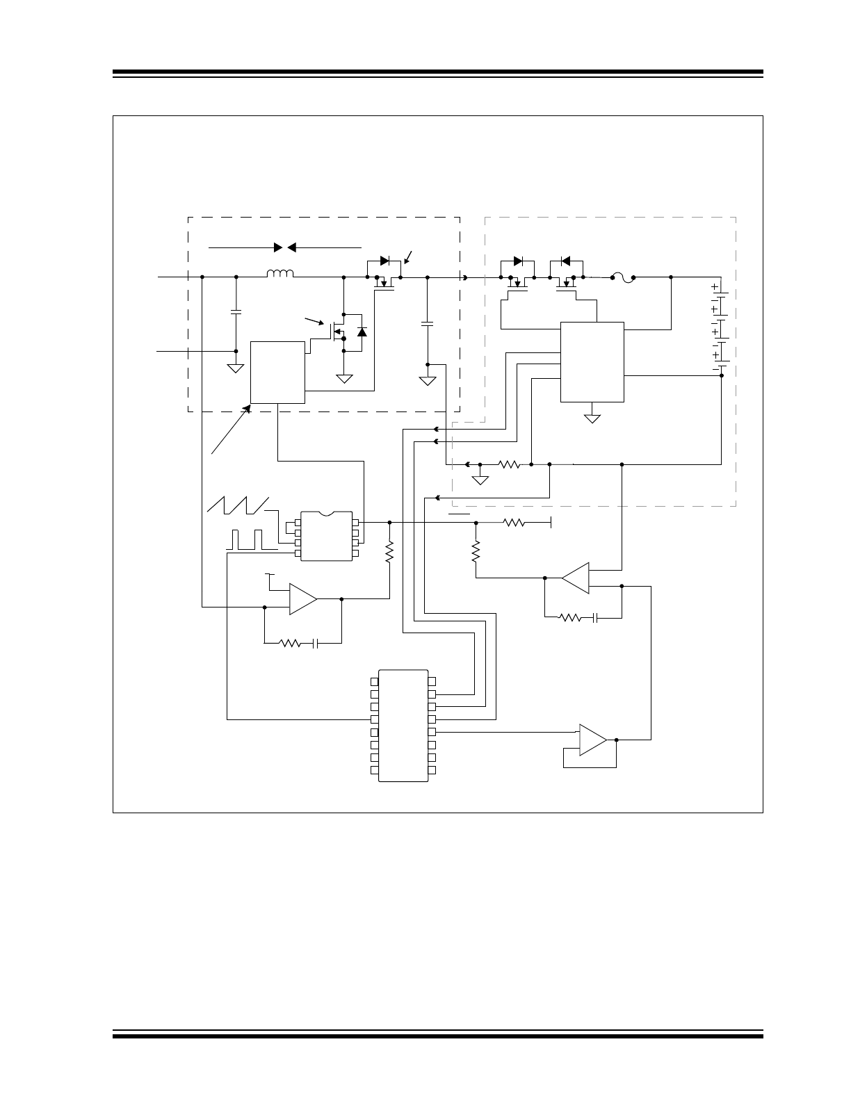
Typical Application Circuit - MCP1630V
Bidirectional Power Converter/Battery Charger for 4-Series Cell Li-Ion Batteries
+
+
Battery
Protection
and
Monitor
+V
BATT
-V
BATT
Bidirectional Buck/Boost
L
C
OUT
C
IN
DC Bus
Voltage
SMBus
4-Cell Li-Ion
Battery Pack
Battery Protection
Switches
R
SENSE
+
–
Boost
Buck
Boost
Switch
Buck
Switch
SMBus
I
SENSE
V
SENSE
Fuse
GND
Sync.
FET
Driver
Comp
FB
CS
V
REF
OSC GND
V
EXT
V
IN
+
–
+
–
+2.5 V
REF
Charge Current Loop
DC bus Voltage Loop
0V to 2.7V
I
REF
Voltage (PWM)
+
–
Filter
+DC Bus V
REF
PIC16F88
MCP1630V
PS501
(1/2) MCP6021
(1/2) MCP6021
(1/2) MCP6021
MCP1630/MCP1630V
DS21896C-page 6
2004-2013 Microchip Technology Inc.
1.0
ELECTRICAL
CHARACTERISTICS
Absolute Maximum Ratings †
V
DD
...................................................................................6.0V
Maximum Voltage on Any Pin .. (V
GND
- 0.3)V to (V
IN
+ 0.3)V
V
EXT
Short Circuit Current ...........................Internally Limited
Storage temperature .....................................-65°C to +150°C
Maximum Junction Temperature, T
J
........................... +150°C
Continuous Operating Temperature Range ..-40°C to +125°C
ESD protection on all pins, HBM
3 kV
† Notice: Stresses above those listed under “Maximum
Ratings” may cause permanent damage to the device. This is
a stress rating only and functional operation of the device at
those or any other conditions above those indicated in the
operational listings of this specification is not implied.
Exposure to maximum rating conditions for extended periods
may affect device reliability.
AC/
AC/DC CHARACTERISTICS
Electrical Specifications: Unless otherwise noted, V
IN
= 3.0V to 5.5V, F
OSC
= 1 MHz with 10% Duty Cycle, C
IN
= 0.1 µF,
V
IN
for typical values = 5.0V, T
A
= -40°C to +125°C.
Parameters
Sym
Min
Typ
Max
Units
Conditions
Input Voltage
Input Operating Voltage
V
IN
3.0
—
5.5
V
Input Quiescent Current
I(V
IN
)
—
2.8
4.5
mA
I
EXT
= 0 mA, F
OSC IN
= 0 Hz
Oscillator Input
External Oscillator Range
F
OSC
—
—
1
MHz
Note 1
Min. Oscillator High Time
Min. Oscillator Low Time
T
OH_MIN
T
OL_MIN
—
10
ns
Oscillator Rise Time
T
RISE
0.01
—
10
µs
Note 2
Oscillator Fall Time
T
FALL
0.01
—
10
µs
Note 2
Oscillator Input Voltage Low
V
L
—
—
0.8
V
Oscillator Input Voltage High
V
H
2.0
—
—
V
Oscillator Input Capacitance
C
OSC
5
pf
External Reference Input
Reference Voltage Input
V
REF
0
—
V
IN
V
Note 2, Note 3
Error Amplifier
Input Offset Voltage
V
OS
-4
0.1
+4
mV
Error Amplifier PSRR
PSRR
80
99
—
dB
V
IN
= 3.0V to 5.0V, V
CM
= 1.2V
Common Mode Input Range
V
CM
GND - 0.3
—
V
IN
V
Note 2, Note 3
Common Mode Rejection Ratio
—
80
—
dB
V
IN
= 5V, V
CM
= 0V to 2.5V
Open-loop Voltage Gain
A
VOL
85
95
—
dB
R
L
= 5 k
to V
IN
/2, 100 mV < V
EAOUT
< V
IN
- 100 mV, V
CM
= 1.2V
Low-level Output
V
OL
—
25
GND + 50
mV
RL = 5 k
to V
IN
/2
Gain Bandwidth Product
GBWP
—
3.5
—
MHz
V
IN
= 5V
Error Amplifier Sink Current
I
SINK
5
11
—
mA
V
IN
= 5V, V
REF
= 1.2V, V
FB
= 1.4V,
V
COMP
= 2.0V
Error Amplifier Source Current
I
SOURCE
-2
-9
—
mA
V
IN
= 5V, V
REF
= 1.2V, V
FB
= 1.0V,
V
COMP
= 2.0V, Absolute Value
Note
1:
Capable of higher frequency operation depending on minimum and maximum duty cycles needed.
2:
External oscillator input (OSC IN) rise and fall times between 10 ns and 10 µs used for characterization testing. Signal
levels between 0.8V and 2.0V with rise and fall times measured between 10% and 90% of maximum and minimum
values. Not production tested.
3:
The reference input of the internal amplifier is capable of rail-to-rail operation.
2004-2013 Microchip Technology Inc.
DS21896C-page 7
MCP1630/MCP1630V
TEMPERATURE SPECIFICATIONS
Current Sense Input
Maximum Current Sense Signal
MCP1630
V
CS_MAX
0.85
0.9
0.95
V
Set by maximum error amplifier
clamp voltage, divided by 3.
Delay From CS to V
EXT
MCP1630
T
CS_VEXT
—
12
25
ns
Maximum Current Sense Signal
MCP1630V
V
CS_MAX
2.55
2.7
2.85
V
V
IN
> 4.25V
Maximum CS input range limited by
comparator input common mode
range. V
CS_MAX
= V
IN
-1.4V
Delay From CS to V
EXT
MCP1630V
T
CS_VEXT
—
17.5
35
ns
Minimum Duty Cycle
DC
MIN
—
—
0
%
V
FB
= V
REF
+ 0.1V,
V
CS
= GND
Current Sense Input Bias Current
I
CS_B
—
-0.1
—
µA
V
IN
= 5V
Internal Driver
R
DSON
P-channel
R
DSon_P
—
10
30
R
DSON
N-channel
R
DSon_N
—
7
30
V
EXT
Rise Time
T
RISE
—
5.9
18
ns
C
L
= 100 pF
Typical for V
IN
= 3V
V
EXT
Fall Time
T
FALL
—
6.2
18
ns
C
L
= 100 pF
Typical for V
IN
= 3V
Protection Features
Under Voltage Lockout
UVLO
2.7
—
3.0
V
V
IN
falling, V
EXT
low state when in
UVLO
Under Voltage Lockout Hysteresis UVLO
HYS
50
75
150
mV
Thermal Shutdown
T
SHD
—
150
—
°C
Thermal Shutdown Hysteresis
T
SHD_HYS
—
18
—
°C
Electrical Specifications: V
IN
= 3.0V to 5.5V, F
OSC
= 1 MHz with 10% Duty Cycle, C
IN
= 0.1 µF. T
A
= -40°C to +125°C.
Parameters
Sym
Min
Typ
Max
Units
Conditions
Temperature Ranges
Operating Junction Temperature Range
T
A
-40
—
+125
°C
Steady state
Storage Temperature Range
T
A
-65
—
+150
°C
Maximum Junction Temperature
T
J
—
—
+150
°C
Transient
Thermal Package Resistances
Thermal Resistance, 8L-DFN
(2 mm x 3 mm)
JA
—
50.8
—
°C/W
Typical 4-layer board with two
interconnecting vias
Thermal Resistance, 8L-MSOP
JA
—
208
—
°C/W
Typical 4-layer board
AC/DC CHARACTERISTICS (CONTINUED)
Electrical Specifications: Unless otherwise noted, V
IN
= 3.0V to 5.5V, F
OSC
= 1 MHz with 10% Duty Cycle, C
IN
= 0.1 µF,
V
IN
for typical values = 5.0V, T
A
= -40°C to +125°C.
Parameters
Sym
Min
Typ
Max
Units
Conditions
Note
1:
Capable of higher frequency operation depending on minimum and maximum duty cycles needed.
2:
External oscillator input (OSC IN) rise and fall times between 10 ns and 10 µs used for characterization testing. Signal
levels between 0.8V and 2.0V with rise and fall times measured between 10% and 90% of maximum and minimum
values. Not production tested.
3:
The reference input of the internal amplifier is capable of rail-to-rail operation.
MCP1630/MCP1630V
DS21896C-page 8
2004-2013 Microchip Technology Inc.
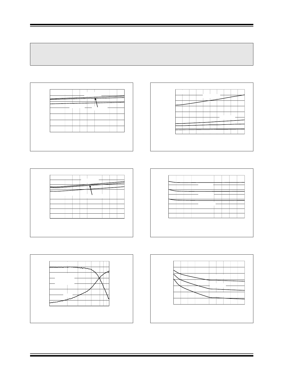
2.0
TYPICAL PERFORMANCE CURVES
Note: Unless otherwise noted, V
IN
= 3.0V to 5.5V, F
OSC
= 1 MHz with 10% Duty Cycle, C
IN
= 0.1 µF, V
IN
for typical
values = 5.0V, T
A
= -40°C to +125°C.
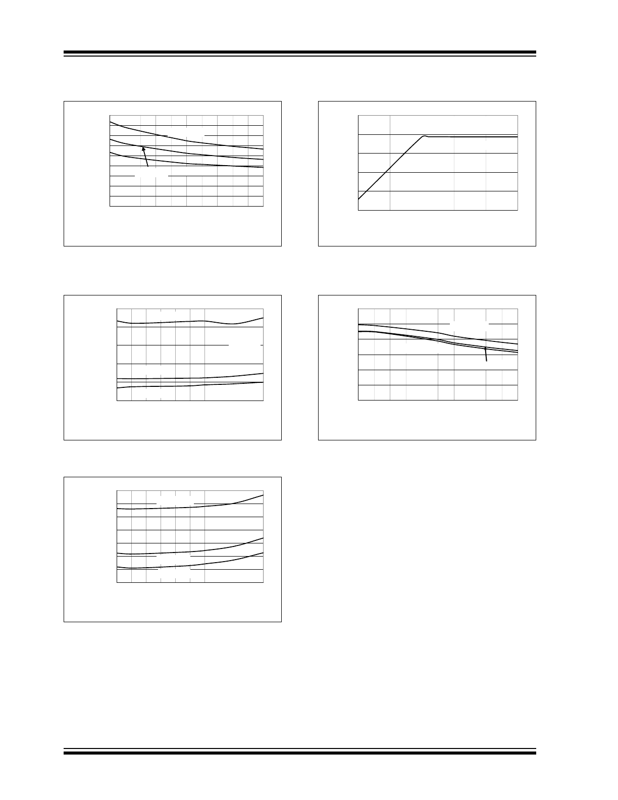
FIGURE 2-1:
Input Quiescent Current vs.
Input Voltage.
FIGURE 2-2:
Input Quiescent Current vs.
Input Voltage.
FIGURE 2-3:
Error Amplifier Frequency
Response.
FIGURE 2-4:
Error Amplifier Input Bias
Current vs. Input Voltage.
FIGURE 2-5:
Error Amplifier Sink Current
vs. Input Voltage.
FIGURE 2-6:
Error Amplifier Source
Current vs. Input Voltage.
Note:
The graphs and tables provided following this note are a statistical summary based on a limited number of
samples and are provided for informational purposes only. The performance characteristics listed herein
are not tested or guaranteed. In some graphs or tables, the data presented may be outside the specified
operating range (e.g., outside specified power supply range) and therefore outside the warranted range.
0
0.5
1
1.5
2
2.5
3
3.5
3
3.25
3.5
3.75
4
4.25
4.5
4.75
5
5.25
5.5
Input Voltage (V)
V
IN
Quiescent C
u
rr
e
nt (mA
)
F
OSC IN
= DC
T
A
= - 40°C
T
A
= + 25°C
T
A
= + 125°C
0
0.5
1
1.5
2
2.5
3
3.5
4
4.5
3
3.25
3.5
3.75
4
4.25
4.5
4.75
5
5.25
5.5
Input Voltage (V)
V
IN
Quiescent C
u
rr
e
nt (m
A
)
F
OSC IN
= 1 MHz
T
A
= - 40°C
T
A
= + 25°C
T
A
= + 125°C
-14
-12
-10
-8
-6
-4
-2
0
2
1000000
10000000
Frequency (Hz)
A
m
plifier
Gain (db)
0
50
100
150
200
250
A
m
plifier
P
h
ase S
h
ift
(degr
ees)
Gain
Phase
V
REF
= 2V
R
LOAD
= 4.7 k
C
LOAD
= 67 pF
1M
10M
5M
-100
0
100
200
300
400
500
600
700
3
3.25
3.5
3.75
4
4.25
4.5
4.75
5
5.25
5.5
Input Voltage (V)
A
m
plifier
Input B
ias C
u
rr
e
nt
(pA
)
V
CM
= V
IN
T
A
= - 40°C
T
A
= + 25°C
T
A
= + 125°C
T
A
= + 85°C
0
2
4
6
8
10
12
14
16
18
3
3.25
3.5
3.75
4
4.25
4.5
4.75
5
5.25
5.5
Input Voltage (V)
A
m
plifier
S
ink C
u
rr
e
nt (mA
)
T
A
= - 40°C
T
A
= + 25°C
T
A
= + 125°C
-14
-12
-10
-8
-6
-4
-2
0
3
3.25
3.5
3.75
4
4.25
4.5
4.75
5
5.25
5.5
Input Voltage (V)
A
m
pl
if
ie
r S
our
ce C
u
rr
e
nt (m
A
)
T
A
= - 40°C
T
A
= + 25°C
T
A
= + 125°C
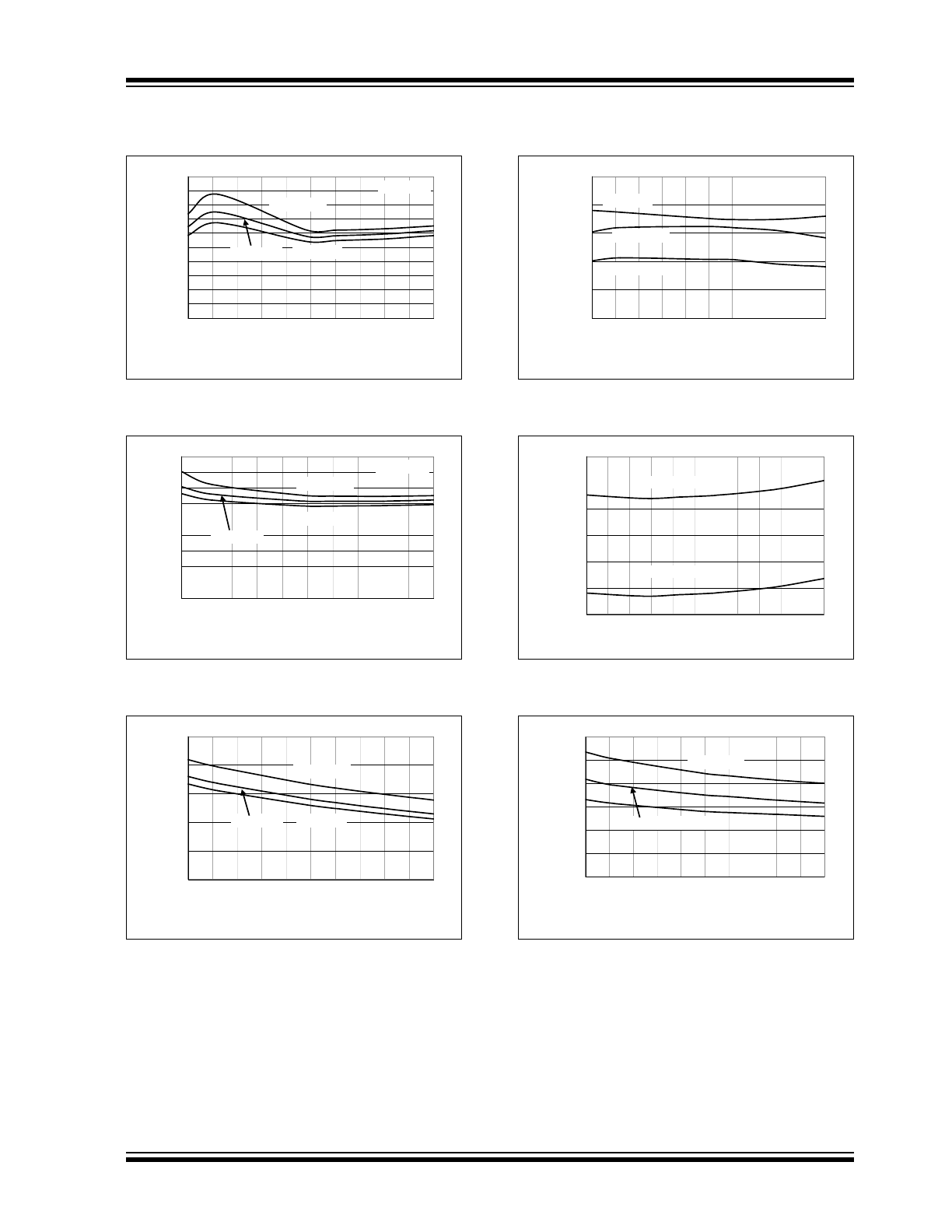
2004-2013 Microchip Technology Inc.
DS21896C-page 9
MCP1630/MCP1630V
Note: Unless otherwise noted, V
IN
= 3.0V to 5.5V, F
OSC
= 1 MHz with 10% Duty Cycle, C
IN
= 0.1 µF, V
IN
for typical
values = 5.0V, T
A
= -40°C to +125°C.
FIGURE 2-7:
V
EXT
Rise Time vs. Input
Voltage.
FIGURE 2-8:
V
EXT
Fall Time vs. Input
Voltage.
FIGURE 2-9:
Current Sense to V
EXT
Delay vs. Input Voltage (MCP1630).
FIGURE 2-10:
Current Sense Clamp
Voltage vs. Input Voltage (MCP1630).
FIGURE 2-11:
Undervoltage Lockout vs.
Temperature.
FIGURE 2-12:
EXT Output N-channel
R
DSON
vs. Input Voltage.
0
1
2
3
4
5
6
7
8
9
10
3
3.25
3.5
3.75
4
4.25
4.5
4.75
5
5.25
5.5
Input Voltage (V)
V
EXT
R
ise Tim
e
(ns)
T
A
= - 40°C
T
A
= + 25°C
T
A
= + 125°C
C
L
= 100 pF
0
1
2
3
4
5
6
7
8
9
3
3.25
3.5
3.75
4
4.25
4.5
4.75
5
5.25
5.5
Input Voltage (V)
V
EXT
F
a
ll T
im
e
(n
s)
T
A
= - 40°C
T
A
= + 25°C
T
A
= + 125°C
C
L
= 100 pF
0
5
10
15
20
25
3
3.25
3.5
3.75
4
4.25
4.5
4.75
5
5.25
5.5
Input Voltage (V)
CS t
o
V
EXT
delay (ns)
T
A
= - 40°C
T
A
= + 25°C
T
A
= + 125°C
0.895
0.896
0.897
0.898
0.899
0.9
3
3.25
3.5
3.75
4
4.25
4.5
4.75
5
5.25
5.5
Input Voltage (V)
C
S
C
lam
p V
o
ltage (V
)
T
A
= - 40°C
T
A
= + 25°C
T
A
= + 125°C
2.84
2.86
2.88
2.90
2.92
2.94
2.96
-40 -25 -10
5
20 35 50 65 80 95 110 125
Ambient Temperature (°C)
U
V
LO
Thr
eshol
d (V
)
Turn On Threshold
Turn Off Threshold
0
2
4
6
8
10
12
3
3.
25
3.
5
3.
75
4
4.
25
4.
5
4.
75
5
5.
25
5.
5
Input Voltage (V)
E
X
T
O
u
tput
N
-C
h
annel
R
DSON
(ohm
s)
T
A
= - 40°C
T
A
= + 25°C
T
A
= + 125°C
MCP1630/MCP1630V
DS21896C-page 10
2004-2013 Microchip Technology Inc.
Note: Unless otherwise noted, V
IN
= 3.0V to 5.5V, F
OSC
= 1 MHz with 10% Duty Cycle, C
IN
= 0.1 µF, V
IN
for typical
values = 5.0V, T
A
= -40°C to +125°C.
FIGURE 2-13:
EXT Output P-channel
R
DSON
vs. Input Voltage.
FIGURE 2-14:
Error Amplifier Input Offset
Voltage vs. Input Voltage.
FIGURE 2-15:
Error Amplifier Input Offset
Voltage vs. Input Voltage.
FIGURE 2-16:
Current Sense Common
Mode Input Voltage Range vs. Input Voltage
(MCP1630V).
FIGURE 2-17:
Current Sense to V
EXT
Delay vs. Input Voltage (MCP1630V).
0
2
4
6
8
10
12
14
16
18
3
3.
25
3.
5
3.
75
4
4.
25
4.
5
4.
75
5
5.
25
5.
5
Input Voltage (V)
EXT O
u
tput
P-
Channel
R
DSON
(O
h
m
s
)
T
A
= - 40°C
T
A
= + 25°C
T
A
= + 125°C
-250
-200
-150
-100
-50
0
3
3.25
3.5
3.75
4
4.25
4.5
4.75
5
5.25
5.5
Input Voltage (V)
E
rr
o
r A
m
p I
nput O
ffset V
o
lt
age
(µV
)
T
A
= - 40°C
T
A
= + 25°C
T
A
= + 125°C
V
CM IN
= 0V
-200
-150
-100
-50
0
50
100
150
3
3.25
3.5
3.75
4
4.25
4.5
4.75
5
5.25
5.5
Input Voltage (V)
E
rr
o
r A
m
p I
nput O
ffset V
o
lt
age
(µV
)
T
A
= - 40°C
T
A
= + 25°C
T
A
= + 125°C
V
CM IN
= 1.2V
1.5
1.8
2.1
2.4
2.7
3
3
3.5
4
4.5
5
5.5
Input Voltage (V)
Max
imu
m C
S
I
n
p
u
t (
V
)
CS Common Mode
Input Range
T
A
= +25°C
0
5
10
15
20
25
30
3
3.25
3.5
3.75
4
4.25
4.5
4.75
5
5.25
5.5
Input Voltage (V)
CS t
o
V
EXT
Delay
(n
s)
T
A
= +25°C
T
A
= +125°C
T
A
= -40°C