
2004-2012 Microchip Technology Inc.
DS21877B-page 1
TC1272A
Features
• Precision V
DD
Monitor
• 140 msec Minimum RESET, Output Duration
• Output Valid to V
DD
= 1.2V
• V
DD
Transient Immunity
• Small 3-Pin SOT-23B Package
• No External Components
Applications
• Computers
• Embedded Systems
• Battery-Powered Equipment
• Critical µP Power Supply Monitoring
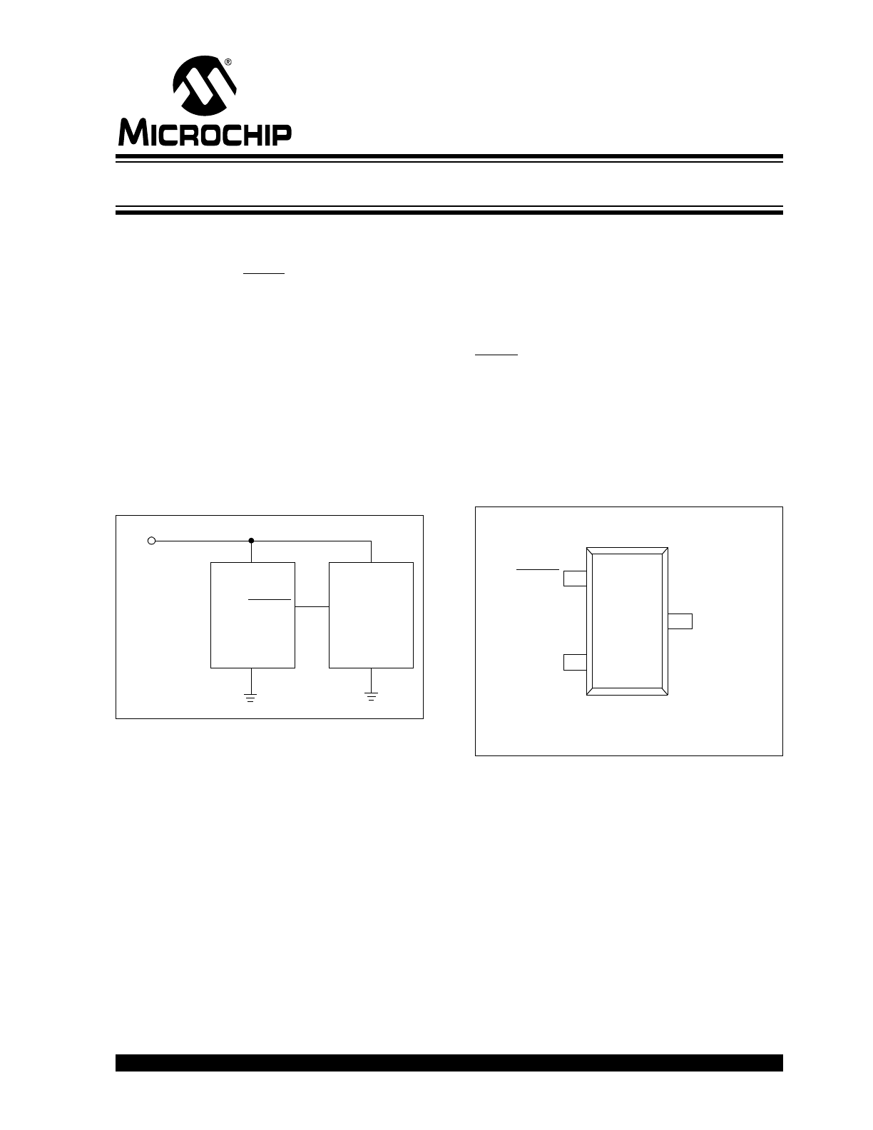
Typical Application Circuit
General Description
The TC1272A are cost-effective system supervisor
circuits designed to monitor V
DD
in digital systems and
provide a reset signal to the host processor, when
necessary. No external components are required.
The reset output is driven active within 65 µsec (typ.)
of V
DD
falling through the reset voltage threshold.
RESET is maintained active for a minimum of
140 msec after V
DD
rises above the reset threshold.
The TC1272A has a complimentary output. The output
of the TC1272A is valid down to V
DD
= 1.2V. The
device is available in a 3-Pin SOT-23B package.
The TC1272A device is optimized to reject fast
transient glitches on the V
DD
line.
Package Type
TC1272A
V
DD
V
DD
V
DD
RESET
RESET
Input
Processor
1
2
3
GND
GND
V
DD
RESET
GND
TC1272A
1
2
3
Note: 3-Pin SOT-23B is equivalent to
3-Pin SOT-23B*
JEDEC TO-236.
3-Pin Reset Monitor
TC1272A
DS21877B-page 2
2004-2012 Microchip Technology Inc.
1.0
ELECTRICAL
CHARACTERISTICS
Absolute Maximum Ratings†
Supply Voltage (V
DD
to GND) ..........................................6.0V
RESET .................................................. –0.3V to (V
DD
+0.3V)
Input Current, V
DD
.........................................................20 mA
Output Current, RESET ................................................20 mA
dV/dt (V
DD
) ............................................................. 100V/µsec
Operating Temperature Range..................... –40°C to +125°C
Power Dissipation (T
A
= 70°C):
3-Pin SOT-23B (derate 4 mW/°C above +70°C) ....320 mW
Storage Temperature Range ........................ –65°C to +150°C
Maximum Junction Temperature, T
J
.............................. 150°C
† Notice: Stresses above those listed under “Maximum
ratings” may cause permanent damage to the device. This is
a stress rating only and functional operation of the device at
those or any other conditions above those indicated in the
operational listings of this specification is not implied. Expo-
sure to maximum rating conditions for extended periods may
affect device reliability.
PIN FUNCTION TABLE
NAME
FUNCTION
GND
Ground
RESET
RESET push-pull output remains
low while V
DD
is below the reset
voltage threshold and for 140 msec
(min.) after V
DD
rises above reset
threshold
V
DD
ELECTRICAL CHARACTERISTICS
V
DD
= Full Range, T
A
= Operating Temperature Range, unless otherwise noted. Typical values are at T
A
= +25°C,
V
DD
= 5V for L/M/J, 3.3V for T/S, 3.0V for R and 2.5V for Z (Note 1).
Parameter
Sym
Min
Typ
Max
Units
Test Conditions
V
DD
Range
1.0
—
5.5
V
T
A
= 0°C to +70°C
1.2
—
5.5
T
A
= – 40°C to +125°C
Supply Current
I
CC
—
12
30
µA
TC1272AL/M/J:
V
DD
< 5.5V
—
9
25
TC1272AR/S/T/Z: V
DD
< 3.6V
Reset Threshold (Note 2)
V
TH
4.56
4.63
4.70
V
TC1272AL:
T
A
= +25°C
4.50
—
4.75
T
A
= – 40°C to +125°C
4.31
4.38
4.45
V
TC1272AM:
T
A
= +25°C
4.25
—
4.50
V
T
A
= – 40°C to +125°C
3.93
4.00
4.06
V
TC1272AJ:
T
A
= +25°C
3.89
—
4.10
V
T
A
= – 40°C to +125°C
3.04
3.08
3.11
V
TC1272AT:
T
A
= +25°C
3.00
—
3.15
V
T
A
= – 40°C to +125°C
2.89
2.93
2.96
V
TC1272AS:
T
A
= +25°C
2.85
—
3.00
V
T
A
= – 40°C to +125°C
2.59
2.63
2.66
V
TC1272AR:
T
A
= +25°C
2.55
—
2.70
V
T
A
= – 40°C to +125°C
2.28
2.32
2.35
V
TC1272AZ:
T
A
= +25°C
2.25
—
2.38
V
T
A
= – 40°C to +125°C
Reset Threshold Tempco
—
30
—
ppm/°C
V
DD
to Reset Delay,
—
65
—
µsec
V
DD
= V
TH
to (V
TH
– 100 mV) (Note 2)
Reset Active Time Out
Period
140
320
560
msec
RESET Output Voltage
Low
V
OL
—
—
0.3
V
TC1272AR/S/T/Z: V
DD
= V
TH
min, I
SINK
= 1.2 mA
—
—
0.4
TC1272AL/M/J:
V
DD
= V
TH
min, I
SINK
= 3.2 mA
—
—
0.3
V
DD
> 1.0V, I
SINK
= 50 µA
RESET Output Voltage
High
V
OH
0.8 V
DD
—
—
V
TC1272AR/S/T/Z: V
DD
> V
TH
max,
I
SOURCE
= 500 µA
V
DD
– 1.5
—
—
TC1272AL/M/J: V
DD
> V
TH
max, I
SOURCE
= 800 µA
Note
1: Production testing done at T
A
= +25°C, overtemperature limits ensured by QC screen.
2: RESET Output for TC1272A.
2004-2012 Microchip Technology Inc.
DS21877B-page 3
TC1272A
2.0
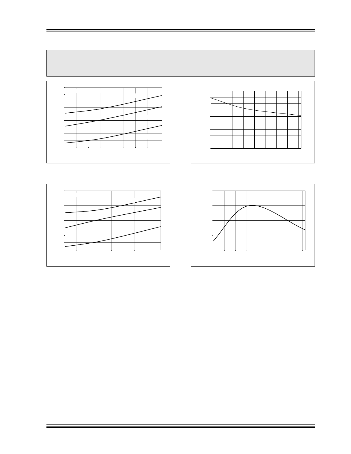
TYPICAL PERFORMANCE CHARACTERISTICS
FIGURE 2-1:
Supply Current vs.
Temperature.
FIGURE 2-2:
Supply Current vs.
Temperature.
FIGURE 2-3:
Power-up Reset Time Out
vs. Temperature.
FIGURE 2-4:
Normalized Reset
Threshold vs. Temperature.
Note:
The graphs and tables provided following this note are a statistical summary based on a limited number of
samples and are provided for informational purposes only. The performance characteristics listed herein
are not tested or guaranteed. In some graphs or tables, the data presented may be outside the specified
operating range (e.g., outside specified power supply range) and therefore outside the warranted range.
0
2
4
6
8
10
12
14
16
18
-40
-20
0
20
40
60
80
100
120
Temperature (°C)
S
uppl
y
C
u
rr
e
nt ( µ
A
)
V
DD
= 1V
V
DD
= 3V
V
DD
= 5V
TC1272A/R/S/T/Z, No Load
0
2
4
6
8
10
12
14
16
-40
-20
0
20
40
60
80
100
120
Temperature (°C)
S
uppl
y
C
u
rr
e
nt ( µ
A
)
V
DD
= 5V
V
DD
= 3V
V
DD
= 1V
TC1272A/L/M/J, No Load
0
50
100
150
200
250
300
350
400
450
-40
-20
0
20
40
60
80
100
120
Temperature (°C)
P
o
w
e
r-
u
p
Reset
T
imeo
u
t (
µ
sec)
0.997
0.998
0.999
1
1.001
-40
-20
0
20
40
60
80
100
120
Temperature (°C)
No
rm
aliz
ed
Reset
T
h
resh
o
ld
TC1272A
DS21877B-page 4
2004-2012 Microchip Technology Inc.
3.0
APPLICATIONS INFORMATION
3.1
V
DD
Transient Rejection
The TC1272A provides accurate V
DD
monitoring and
reset timing during power-up, power-down and brown-
out/sag conditions. These devices also reject negative-
going transients (glitches) on the power supply line.
Figure 3-1 shows the maximum transient duration vs.
maximum negative excursion (overdrive) for glitch
rejection. Any combination of duration and overdrive
that lies under the curve will not generate a reset
signal.
FIGURE 3-1:
Maximum Transient
Duration vs. Overdrive for Glitch Rejection at
+25°C.
Combinations above the curve are detected as a
brown-out or power-down condition. Transient immu-
nity can be improved by adding a capacitor in close
proximity to the V
DD
pin of the TC1272A.
3.2
RESET Signal Integrity During
Power-Down
The TC1272A RESET output is valid to V
DD
= 1.0V.
Below this voltage, the output becomes an "open cir-
cuit" and does not sink current. This means CMOS
logic inputs to the microcontroller will be floating at an
undetermined voltage. Most digital systems are com-
pletely shut down well above this voltage. However, in
situations where RESET must be maintained valid to
V
DD
= 0V, a pull-down resistor must be connected from
RESET to ground to discharge stray capacitances and
hold the output low (Figure 3-2). This resistor value,
though not critical, should be chosen such that it does
not appreciably load RESET under normal operation
(100 k
will be suitable for most applications).
FIGURE 3-2:
The addition of R
1
at the
RESET output of the TC1272A ensures that the
RESET output is valid to V
DD
= 0V.
Reset Comparator Overdrive
[V
TH
- V
DD
] (mv)
400
240
160
320
80
0
1
5
100
1000
T
A
= +25°C
V
TH
Duration
Overdrive
V
DD
TC1272A/L/M/J
M
axi
m
u
m
T
ran
si
en
t
Du
rati
o
n
(µ
sec)
TC1272A/Z/R/S/T
[V
TH
- V
DD
] (mv)
30
40
50
60
70
80
90
100
110
120
130
1
10
100
1000
Reset Comparator Overdrive (mV)
V
DD
t
o
R
e
set
D
e
lay (
µ
sec
)
TC1272A/L/M/J
TC1272A/Z/R/S/T
TC1272A
V
DD
V
DD
R
1
100 k
RESET
GND
2004-2012 Microchip Technology Inc.
DS21877B-page 5
TC1272A
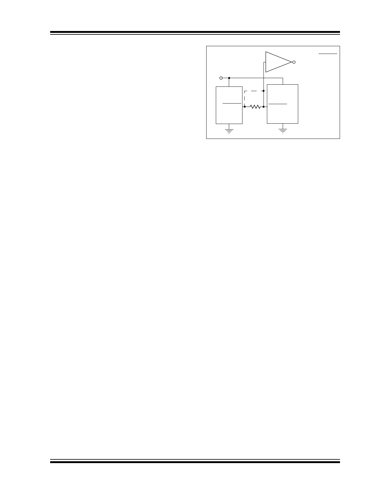
3.3
Controllers and Processors With
Bidirectional I/O Pins
Some microcontrollers have bidirectional reset pins.
Depending on the current drive capability of the
controller pin, an indeterminate logic level may result if
there is a logic conflict. This can be avoided by adding
a 4.7 k
resistor in series with the output of the
TC1272A (Figure 3-3). If there are other components in
the system that require a reset signal, they should be
buffered so as not to load the reset line. If the other
components are required to follow the reset I/O of the
microcontroller, the buffer should be connected as
shown with the solid line.
FIGURE 3-3:
Interfacing the TC1272A to
a Bidirectional RESET I/O.
TC1272A
V
DD
RESET
GND
RESET
GND
Buffered RESET
To Other System
Components
4.7 k
Buffer
Micro-
TC1272A
RESET
GND
RESET
GND
Buffered RESET
To Other System
Components
PIC
®
4.7 k
Buffer
MCU
TC1272A
DS21877B-page 6
2004-2012 Microchip Technology Inc.
4.0
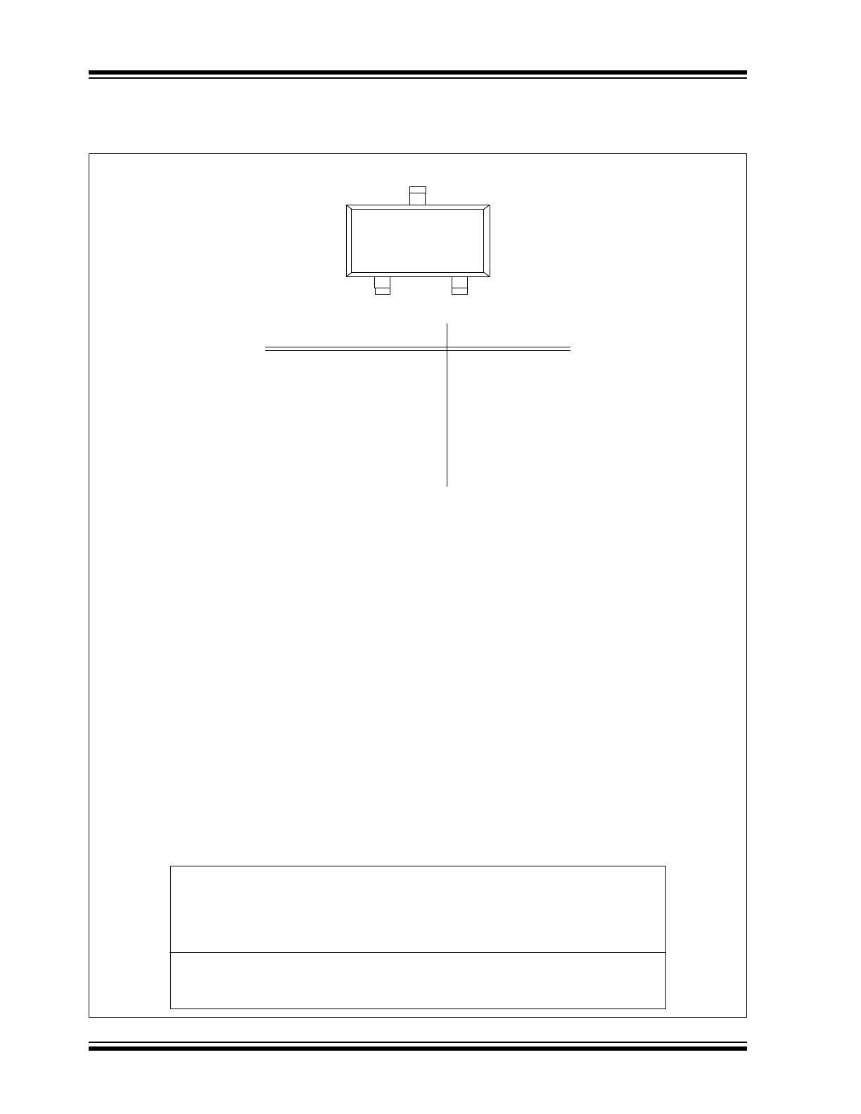
PACKAGING INFORMATION
4.1
Package Marking Information
Part Number
SOT-23
TC1272AZVNBTR
BA
TC1272ARVNBTR
BB
TC1272ASVNBTR
BC
TC1272ATVNBTR
BD
TC1272AJVNBTR
BE
TC1272AMVNBTR
BF
TC1272ALVNBTR
BG
Legend: 1
Part Number + temperature range and voltage (two-digit code)
2
Part Number + temperature range and voltage (two-digit code)
3
Lot ID number
4
Year and work week
5
Year and work week
6
Year and work week
Note:
In the event the full Microchip part number cannot be marked on one line, it will be
carried over to the next line thus limiting the number of available characters for customer
specific information.
3-Pin SOT-23B
2004-2012 Microchip Technology Inc.
DS21877B-page 7
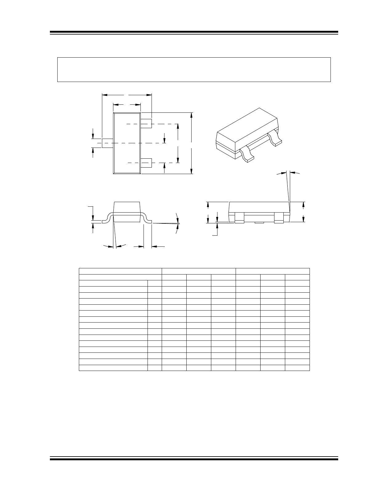
TC1272A
3-Lead Plastic Small Outline Transistor (NB) (SOT-23)
10
5
0
10
5
0
Mold Draft Angle Bottom
10
5
0
10
5
0
Mold Draft Angle Top
0.51
0.44
0.37
.020
.017
.015
B
Lead Width
0.18
0.14
0.09
.007
.006
.004
c
Lead Thickness
10
5
0
10
5
0
Foot Angle
0.55
0.45
0.35
.022
.018
.014
L
Foot Length
3.04
2.92
2.80
.120
.115
.110
D
Overall Length
1.40
1.30
1.20
.055
.051
.047
E1
Molded Package Width
2.64
2.37
2.10
.104
.093
.083
E
Overall Width
0.10
0.06
0.01
.004
.002
.000
A1
Standoff
§
1.02
0.95
0.88
.040
.037
.035
A2
Molded Package Thickness
1.12
1.01
0.89
.044
.040
.035
A
Overall Height
1.92
.076
p1
Outside lead pitch (basic)
0.96
.038
p
Pitch
3
3
n
Number of Pins
MAX
NOM
MIN
MAX
NOM
MIN
Dimension Limits
MILLIMETERS
INCHES*
Units
2
1
p
D
B
n
E
E1
L
c
A2
A
A1
p1
* Controlling Parameter
Notes:
Dimensions D and E1 do not include mold flash or protrusions. Mold flash or protrusions shall not exceed
.010” (0.254mm) per side.
JEDEC Equivalent: TO-236
Drawing No. C04-104
§ Significant Characteristic
Note:
For the most current package drawings, please see the Microchip Packaging Specification located
at http://www.microchip.com/packaging
TC1272A
DS21877B-page 8
2004-2012 Microchip Technology Inc.
4.2
Product Tape and Reel Specifications
FIGURE 4-1:
EMBOSSED CARRIER DIMENSIONS (8, 12, 16, AND 24 MM TAPE ONLY)
FIGURE 4-2:
3-LEAD SOT-23 DEVICE TAPE AND REEL SPECIFICATIONS
Top
Cover
Tape
K
0
P
W
B
0
A
0
TABLE 1:
CARRIER TAPE/CAVITY DIMENSIONS
Case
Outline
Package
Type
Carrier
Dimensions
Cavity
Dimensions
Output
Quantity
Units
Reel
Diameter in
mm
W
mm
P
mm
A0
mm
B0
mm
K0
mm
NB
SOT-23
3L
8
4
3.15
2.77
1.22
3000
180
User Direction of Feed
P,
Pitch
Standard Reel Component Orientation
Reverse Reel Component Orientation
W, Width
of Carrier
Tape
Pin 1
Pin 1
Device
Marking
Devic
e
Marki
ng

2004-2012 Microchip Technology Inc.
DS21877B-page 9
TC1272A
5.0
REVISION HISTORY
Revision B (January 2013)
Added a note to each package outline drawing.

TC1272A
DS21877B-page 10
2004-2012 Microchip Technology Inc.
NOTES: