
2004-2013 Microchip Technology Inc.
DS21876B-page 1
MCP1650/51/52/53
Features
• Output Power Capability Over 5 Watts
• Output Voltage Capability From 3.3V to Over
100V
• 750 kHz Gated Oscillator Switching Frequency
• Adaptable Duty Cycle for Battery or Wide-Input,
Voltage-Range Applications
• Input Voltage Range: 2.0V to 5.5V
• Capable of SEPIC and Flyback Topologies
• Shutdown Control with I
Q
< 0.1 µA (Typical)
• Low Operating Quiescent Current: I
Q
= 120 µA
• Voltage Feedback Tolerance (0.6%, Typical)
• Popular MSOP-8 Package
• Peak Current Limit Feature
• Two Undervoltage Lockout (UVLO) Options:
- 2.0V or 2.55V
• Operating Temperature Range: -40°C to +125°C
Applications
• High-Power Boost Applications
• High-Voltage Bias Supplies
• White LED Drivers and Flashlights
• Local 3.3V to 5.0V Supplies
• Local 3.3V to 12V Supplies
• Local 5.0V to 12V Supplies
• LCD Bias Supply
Description
The MCP1650/51/52/53 is a 750 kHz gated oscillator
boost controller packaged in an 8 or 10-pin MSOP
package. Developed for high-power, portable applica-
tions, the gated oscillator controller can deliver 5 watts
of power to the load while consuming only 120 µA of
quiescent current at no load. The MCP1650/51/52/53
can operate over a wide input voltage range (2.0V to
5.5V) to accommodate multiple primary-cell and single-
cell Li-Ion battery-powered applications, in addition to
2.8V, 3.3V and 5.0V regulated input voltages.
An internal 750 kHz gated oscillator makes the
MCP1650/51/52/53 ideal for space-limited designs.
The high switching frequency minimizes the size of the
external inductor and capacitor, saving board space
and cost. The internal oscillator operates at two differ-
ent duty cycles depending on the level of the input volt-
age. By changing duty cycle in this fashion, the peak
input current is reduced at high input voltages, reducing
output ripple voltage and electrical stress on power
train components. When the input voltage is low, the
duty cycle changes to a larger value in order to provide
full-power capability at a wide input voltage range
typical of battery-powered, portable applications.
The MCP1650/51/52/53 was designed to drive external
switches directly using internal low-resistance
MOSFETs.
Additional features integrated on the MCP1650/51/52/
53 family include peak input current limit, adjustable
output voltage/current, low battery detection and
power-good indication.
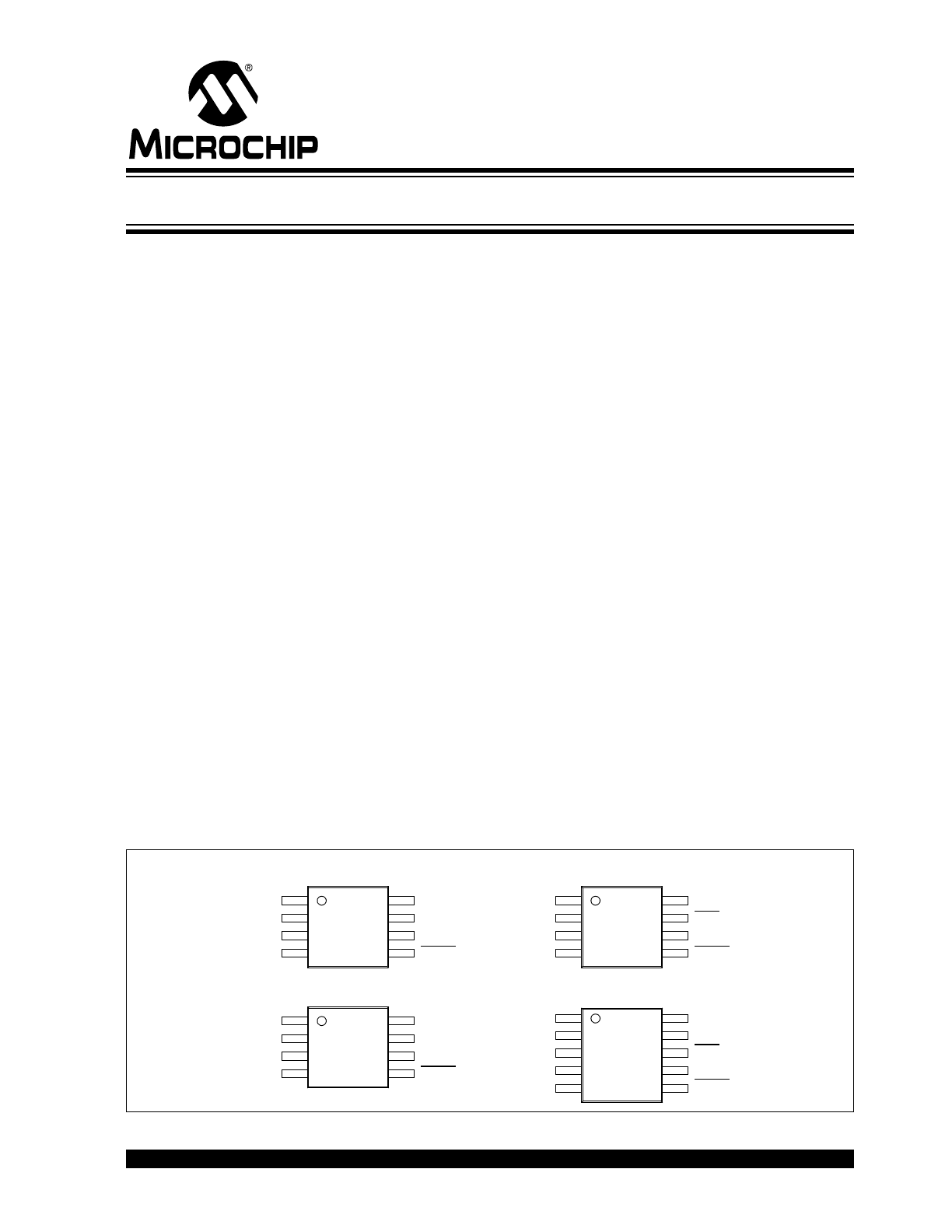
Package Types
10-Pin MSOP
EXT
GND
CS
FB
V
IN
NC
NC
SHDN
1
2
3
4
8
7
6
5
MCP
1
6
5
0
8-Pin MSOP
GND
CS
FB
NC
PG
LBO
LBI
SHDN
2
3
4
5
9
8
7
6
MCP
1
6
5
3
EXT
V
IN
1
10
EXT
GND
CS
FB
V
IN
PG
NC
SHDN
1
2
3
4
8
7
6
5
M
C
P
1652
8-Pin MSOP
EXT
GND
CS
FB
V
IN
LBO
LBI
SHDN
1
2
3
4
8
7
6
5
MCP
1
6
5
1
8-Pin MSOP
750 kHz Boost Controller
MCP1650/51/52/53
DS21876B-page 2
2004-2013 Microchip Technology Inc.
MCP1650 Block Diagram
ISNS
+
-
1.22V
1R
9R
+
-
+
-
Internal Osc. with
2 fixed Duty Cycles
V
HIGH
V
LOW
V
DUTY
+
-
V
REF
V
IN
V
HIGH
V
LOW
V
DUTY
DC = 80% V
IN
< 3.8V
DC = 56% V
IN
> 3.8V
V
IN
+
-
Voltage Feedback
Current Limit
CS
V
IN
EXT
Osc.
SHDN
FB
V
REF
1.22V
S
R
Q
Pulse
DR
Soft-
Start
ON/
OSC. OUT
GND
ON/OFF
Control
MCP1650
Latch
Ref
0.122V
OFF
2004-2013 Microchip Technology Inc.
DS21876B-page 3
MCP1650/51/52/53
MCP1651/2/3 Block Diagram
Vin
CS
EXT
MCP1650/51/52/53
SHDN
GND
+
-
Low Battery
Comparator
1.22 Vref
LBI
LBO
+
-
Power Good
Comparators
PG
85% of Vref
VIN
+
-
115% of Vref
VIN
MCP1651 - Low Battery Detection
MCP1652 - Power Good Indication
A
MCP1650 - No Features
MCP1651 - Low Battery Detection
MCP1652 - Power Good Indication
MCP1653 - Low Battery Detection and PG
MCP1650
V
FB
Vref. (1.22V)
MCP1653 - LBI and PG Features
MCP1650/51/52/53
DS21876B-page 4
2004-2013 Microchip Technology Inc.
Timing Diagram
Typical Application Circuits
Latch Truth Table
S
R
Q
0
0
Qn
0
1
1
1
0
0
1
1
1
Osc
S
R
Q
DR
EXT
MCP1650/1/2/3 Timing Diagram
R
S
Q
Q
FB
CS
SHDN
V
IN
8
2
5
6
4
7
MCP1650
GND
Input
Voltage
3.3V ±10%
C
IN
10 µF
off
on
EXT
Boost
Inductor
3.3 µH
10 µF
Ceramic
90.9 k
V
OUT
= 12V
I
OUT
= 0 to 100 mA
10 k
MOSFET/Schottky
Combination Device
R
SENSE
0.05
3.3V to 12V 100 mA Boost Converter
1
3
NC
NC
C
OUT
2004-2013 Microchip Technology Inc.
DS21876B-page 5
MCP1650/51/52/53
1.0
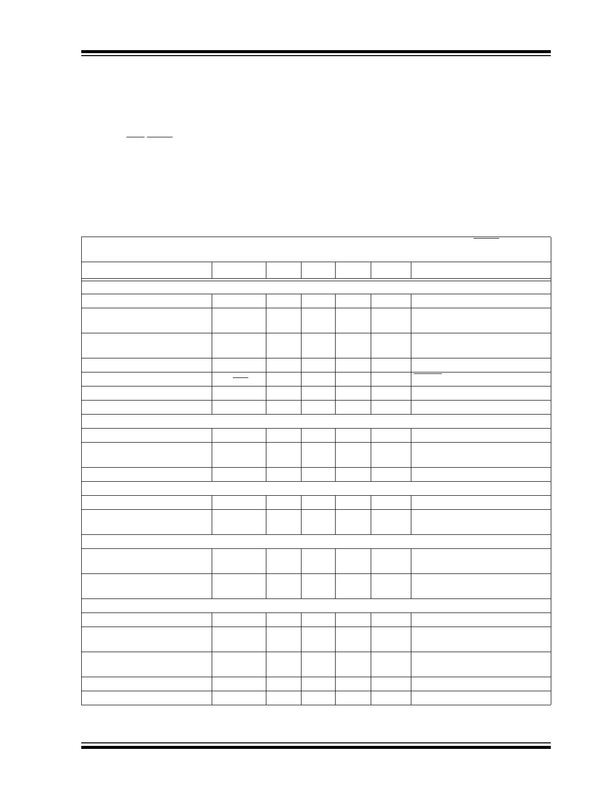
ELECTRICAL
CHARACTERISTICS
Absolute Maximum Ratings †
V
IN
TO
GND........................................................... 6.0V
CS,FB,LBI,LBO,SHDN,PG,EXT ............ GND – 0.3V to
V
IN
+ 0.3V
Current at EXT pin ................................................ ±1A
Storage temperature .......................... -65°C to +150°C
Operating Junction Temperature........ -40°C to +125°C
ESD protection on all pins
4 kV HBM
† Notice: Stresses above those listed under “Maximum Rat-
ings” may cause permanent damage to the device. This is a
stress rating only and functional operation of the device at
those or any other conditions above those indicated in the
operational listings of this specification is not implied. Expo-
sure to maximum rating conditions for extended periods may
affect device reliability.
DC CHARACTERISTICS
Electrical Specifications: Unless otherwise noted, all parameters apply at V
IN
= +2.7V to +5.5V, SHDN = High,
T
J
= -40°C to +125°C. Typical values apply for V
IN
= 3.3V, T
A
+25°C.
Parameters
Sym
Min
Typ
Max
Units
Conditions
Input Characteristics
Supply Voltage
V
IN
2.7
—
5.5
V
Undervoltage Lockout
(S Option)
UVLO
2.4
2.55
2.7
V
V
IN
rising edge
Under Voltage Lockout
(R Option)
UVLO
1.85
2.0
2.15
V
V
IN
rising edge
Undervoltage Hysteresis
UVLO
HYST
—
117
—
mV
Shutdown Supply Current
I
SHD
—
0.001
1
µA
SHDN = GND
Quiescent Supply Current
I
Q
—
120
220
µA
EXT = Open
Soft Start Time
T
SS
—
500
—
µs
Feedback Characteristics
Feedback Voltage
V
FB
1.18
1.22
1.26
V
All conditions
Feedback Comparator
Hysteresis
V
HYS
—
12
23
mV
Feedback Input Bias Current
I
FBlk
-50
—
50
nA
V
FB
< 1.3V
Current Sense Input
Current Sense Threshold
I
SNS-TH
75
114
155
mV
Delay from Current Sense to
Output
T
dly_ISNS
—
80
—
ns
Ext Drive
EXT Driver ON Resistance
(High Side)
R
HIGH
—
8
18
EXT Driver ON Resistance
(Low Side)
R
LOW
—
4
12
Oscillator Characteristics
Switching Frequency
F
OSC
650
750
850
kHz
Low Duty Cycle Switch-Over
Voltage
V
LowDuty
—
3.8
—
V
V
IN
rising edge
Duty Cycle Switch Voltage
Hysteresis
DC
Hyst
—
92
—
mV
Low Duty Cycle
DC
LOW
50
56
62
%
High Duty Cycle
DC
HIGH
72
80
88
%
MCP1650/51/52/53
DS21876B-page 6
2004-2013 Microchip Technology Inc.
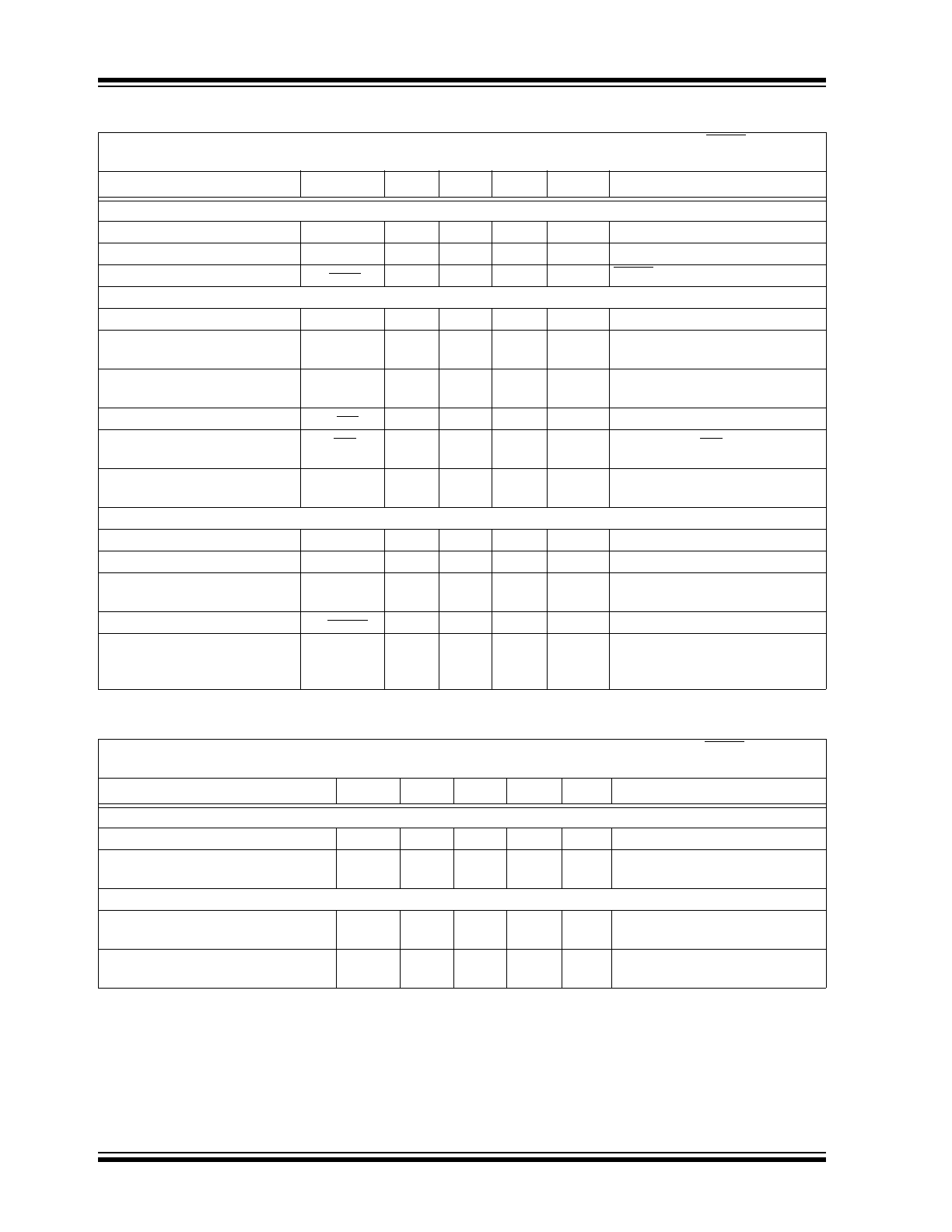
TEMPERATURE SPECIFICATIONS
Shutdown Input
Logic High Input
V
IN-HIGH
50
—
—
% of V
IN
Logic Low Input
V
IN-Low
—
—
15
% of V
IN
Input Leakage Current
I
SHDN
—
5
100
nA
SHDN=V
IN
Low Battery Detect (MCP1651/MCP1653 Only)
Low Battery Threshold
LBI
TH
1.18
1.22
1.26
V
LBI Input falling (All Conditions)
Low Battery Threshold
Hysteresis
LBI
THHYS
95
123
145
mV
Low Battery Input Leakage
Current
I
LBI
—
10
—
nA
V
LBI
= 2.5V
Low Battery Output Voltage
V
LBO
—
53
200
mV
I
LB
SINK = 3.2 mA, V
LBI
= 0V
Low Battery Output Leakage
Current
I
LBO
—
0.01
1
µA
V
LBI
= 5.5V, V
LBO
= 5.5V
Time Delay from LBI to LBO
T
D_LBO
—
70
—
µs
L
BI
Transitions from
L
BITH
+ 0.1V to L
BITH
- 0.1V
Power Good Output (MCP1652/MCP1653 Only)
Power Good Threshold Low
V
PGTH-L
-20
-15
-10
%
Referenced to Feedback Voltage
Power Good Threshold High
V
PGTH-H
+10
+15
+20
%
Referenced to Feedback Voltage
Power Good Threshold
Hysteresis
V
PGTH-HYS
—
5
—
%
Referenced to Feedback Voltage
(Both Low and High Thresholds)
Power Good Output Voltage
V
PGOUT
—
53
200
mV
I
PG
SINK = 3.2 mA, V
FB
= 0V
Time Delay from V
FB
out of
regulation to Power Good
Output transition
T
D_PG
—
85
—
µs
V
FB
Transitions from
V
FBTH
+ 0.1V to V
FBTH
-0.1V
Electrical Specifications: Unless otherwise noted, all parameters apply at V
IN
= +2.7V to +5.5V, SHDN = High,
T
A
= -40°C to +125°C. Typical values apply for V
IN
= 3.3V, T
A
= +25°C.
Parameters
Sym
Min
Typ
Max
Units
Conditions
Temperature Ranges
Storage Temperature Range
T
A
-40
—
+125
°C
Operating Junction Temperature
Range
T
J
-40
—
+125
°C
Continuous
Thermal Package Resistances
Thermal Resistance, MSOP-8
JA
—
208
—
°C/W
Single-Layer SEMI G42-88
Board, Natural Convection
Thermal Resistance, MSOP-10
JA
—
113
—
°C/W
4-Layer JC51-7 Standard Board,
Natural Convection
DC CHARACTERISTICS (CONTINUED)
Electrical Specifications: Unless otherwise noted, all parameters apply at V
IN
= +2.7V to +5.5V, SHDN = High,
T
J
= -40°C to +125°C. Typical values apply for V
IN
= 3.3V, T
A
+25°C.
Parameters
Sym
Min
Typ
Max
Units
Conditions
2004-2013 Microchip Technology Inc.
DS21876B-page 7
MCP1650/51/52/53
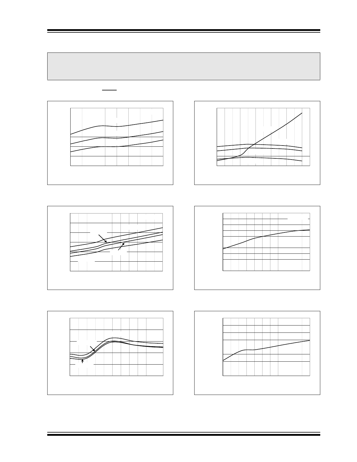
2.0
TYPICAL PERFORMANCE CURVES
Note: Unless otherwise indicated,
V
IN
= 3.3V, V
OUT
= 12V, C
IN
= 10 µF (x5R or X7R Ceramic), C
OUT
= 10 µF (X5R or X7R),
I
OUT
= 10 mA, L = 3.3 µH, SHDN > V
IH
, T
A
= +25°C.
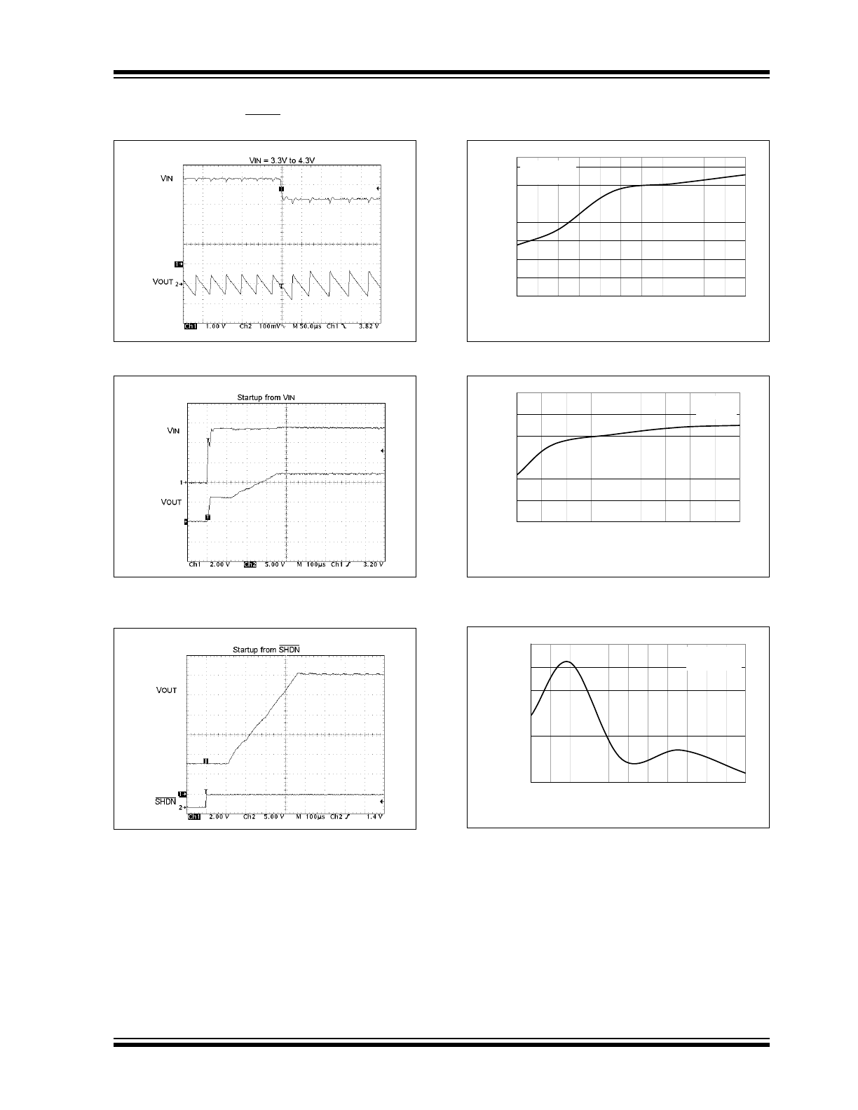
FIGURE 2-1:
Input Quiescent Current vs.
Input Voltage.
FIGURE 2-2:
Input Quiescent Current vs.
Ambient Temperature.
FIGURE 2-3:
Oscillator Frequency vs.
Input Voltage.
FIGURE 2-4:
Oscillator Frequency vs.
Ambient Temperature.
FIGURE 2-5:
Duty Cycle Switch-Over
Voltage vs. Ambient Temperature.
FIGURE 2-6:
Duty Cycle Switch-Over
Hysteresis Voltage vs. Ambient Temperature.
Note:
The graphs and tables provided following this note are a statistical summary based on a limited number of
samples and are provided for informational purposes only. The performance characteristics listed herein
are not tested or guaranteed. In some graphs or tables, the data presented may be outside the specified
operating range (e.g., outside specified power supply range) and therefore outside the warranted range.
50
75
100
125
150
175
200
2
2.5
3
3.5
4
4.5
5
5.5
6
Input Voltage (V)
Input Quiescent C
u
rr
e
nt (µA
)
T
J
= - 40°C
T
J
= +25°C
T
J
= +125°C
I
LOAD
= 0 mA
50
75
100
125
150
175
200
-40
-25
-10
5
20
35
50
65
80
95
110 125
Ambient Temperature (°C)
Input Quiescent C
u
rr
e
nt (µA
)
V
IN
= 2.0V
I
LOAD
= 0 mA
V
IN
= 5.5V
V
IN
= 4.1V
V
IN
= 2.7V
700
720
740
760
780
800
2.7
3
3.3
3.6
3.9
4.2
4.5
4.8
5.1
5.4
5.7
6
Input Voltage (V)
Oscillato
r F
req
u
e
n
cy (kHz)
T
J
= - 40°C
T
J
= +25°C
T
J
= +125°C
720
740
760
780
800
820
840
-40 -25 -10
5
20
35
50
65
80
95 110 125 140
Ambient Temperature (°C)
Oscillato
r F
req
u
e
n
cy (kHz)
V
IN
= 2.0V
V
IN
= 5.5V
V
IN
= 4.1V
V
IN
= 2.7V
3.75
3.76
3.77
3.78
3.79
3.80
3.81
3.82
3.83
3.84
3.85
-40 -25 -10
5
20
35
50
65
80
95
110 125
Ambient Temperature (°C)
D
u
ty C
ycle S
w
itch Over
V
o
ltage (V
)
V
IN
= Rising
90.0
90.5
91.0
91.5
92.0
92.5
93.0
93.5
94.0
-40 -25 -10
5
20
35
50
65
80
95
110 125
Ambient Temperature (°C)
D
u
ty C
ycle S
w
itch V
o
ltage
H
yster
esis (m
V
)
MCP1650/51/52/53
DS21876B-page 8
2004-2013 Microchip Technology Inc.
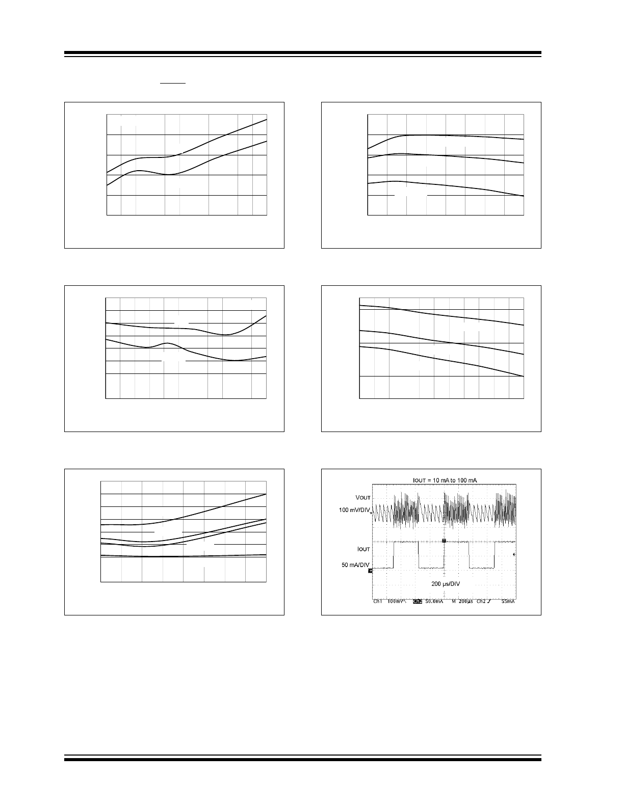
Note: Unless otherwise indicated,
V
IN
= 3.3V, VOUT = 12V, C
IN
= 10 µF (x5R or X7R Ceramic), C
OUT
= 10 µF (X5R or X7R),
I
OUT
= 10 mA, L = 3.3 µH, SHDN > V
IH
, T
A
= +25°C.
FIGURE 2-7:
EXT Sink and Source
Current vs. Input Voltage.
FIGURE 2-8:
EXT Sink and Source
Current vs. Ambient Temperature.
FIGURE 2-9:
EXT Rise and Fall Times vs.
External Capacitance.
FIGURE 2-10:
Feedback Voltage vs. Input
Voltage.
FIGURE 2-11:
Feedback Voltage
Hysteresis vs. Input Voltage.
FIGURE 2-12:
Dynamic Load Response.
0.0
0.2
0.4
0.6
0.8
1.0
2.7
3.0
3.3
3.6
3.9
4.2
4.5
4.8
5.1
5.4
5.7
6.0
Input Voltage (V)
E
X
T
S
ink/
S
our
ce C
u
rr
e
nt (A
)
I
SINK
I
SOURCE
T
A
= +25°C
0.0
0.1
0.2
0.3
0.4
0.5
0.6
0.7
0.8
-40
-25
-10
5
20
35
50
65
80
95
110 125
Ambient Temperature (°C)
E
X
T
S
ink/
S
our
ce C
u
rr
e
nt (A
)
I
SINK
I
SOURCE
V
IN
= 3.3V
0
10
20
30
40
50
60
70
80
100
150
200
250
300
350
400
450
500
External Capacitance (pF)
E
X
T
Rise / F
a
ll T
im
e
(n
S
)
5V
FALL
2.7V
RISE
5V
RISE
2.7V
FALL
1.205
1.210
1.215
1.220
1.225
1.230
2
2.5
3
3.5
4
4.5
5
5.5
6
Input Voltage (V)
V
FB
V
o
ltage (V
)
T
J
= - 40°C
T
J
= +25°C
T
J
= +125°C
0
2
4
6
8
10
12
14
16
18
2.7
3
3.3
3.6
3.9
4.2
4.5
4.8
5.1
5.4
5.7
6
Input Voltage (V)
V
FB
H
yster
esis (m
V
)
T
J
= - 40°C
T
J
= +25°C
T
J
= +125°C
2004-2013 Microchip Technology Inc.
DS21876B-page 9
MCP1650/51/52/53
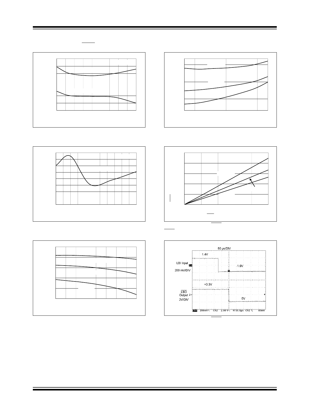
Note: Unless otherwise indicated,
V
IN
= 3.3V, VOUT = 12V, C
IN
= 10 µF (x5R or X7R Ceramic), C
OUT
= 10 µF (X5R or X7R),
I
OUT
= 10 mA, L = 3.3 µH, SHDN > V
IH
, T
A
= +25°C.
FIGURE 2-13:
Dynamic Line Response.
FIGURE 2-14:
Power-Up Timing (Input
Voltage).
FIGURE 2-15:
Power-Up Timing
(Shutdown).
FIGURE 2-16:
Efficiency vs. Input Voltage.
FIGURE 2-17:
Efficiency vs. Load Current.
FIGURE 2-18:
Output Voltage vs. Input
Voltage (Line Regulation).
75
77
79
81
83
85
87
89
2.7
3.0
3.3
3.6
3.9
4.2
4.5
4.8
5.1
5.4
5.7
6.0
Input Votlage (V)
E
fficiency (%
)
T
A
= 25°C
I
OUT
= 100 mA
60
65
70
75
80
85
90
10.0
20.0
30.0
40.0
50.0
60.0
70.0
80.0
90.0
100.0
Load Current (mA)
E
fficiency (%
)
T
A
= 25°C
V
IN
= 3.3V
12.10
12.11
12.12
12.13
12.14
12.15
12.16
2.7
3.0
3.3
3.6
3.9
4.2
4.5
4.8
5.1
5.4
5.7
6.0
Input Voltage (V)
Output V
o
ltage (V
)
T
A
= 25°C
I
OUT
= 100 mA
MCP1650/51/52/53
DS21876B-page 10
2004-2013 Microchip Technology Inc.
Note: Unless otherwise indicated,
V
IN
= 3.3V, VOUT = 12V, C
IN
= 10 µF (x5R or X7R Ceramic), C
OUT
= 10 µF (X5R or X7R),
I
OUT
= 10 mA, L = 3.3 µH, SHDN > V
IH
, T
A
= +25°C.
FIGURE 2-19:
Output Voltage vs. Output
Current (Load Regulation).
FIGURE 2-20:
Output Voltage Ripple vs.
Input Voltage.
FIGURE 2-21:
LBI Threshold Voltage vs.
Input Voltage.
FIGURE 2-22:
LBI Hysteresis Voltage vs.
Input Voltage.
FIGURE 2-23:
LBO Output Voltage vs.
LBO Sink Current.
FIGURE 2-24:
LBO Output Timing.
12.10
12.11
12.12
12.13
12.14
12.15
12.16
12.17
10
20
30
40
50
60
70
80
90
100
Output Current (mA)
Output V
o
ltage (V
)
V
IN
= 3.3V
T
A
= +25°C
V
IN
= 4.3V
0.10
0.12
0.14
0.16
0.18
0.20
0.22
0.24
0.26
2.7
3.0
3.3
3.6
3.9
4.2
4.5
4.8
5.1
5.4
5.7
6.0
Input Voltage (V)
V
OUT
R
ippl
e
PK-PK
(V
)
I
OUT
= 100mA
T
A
= +25°C
1.205
1.210
1.215
1.220
1.225
1.230
2
2.5
3
3.5
4
4.5
5
5.5
6
Input Voltage (V)
LB
I Thr
eshol
d V
o
lt
age (V
)
T
J
= - 40°C
T
J
= +25°C
T
J
= +125°C
120
121
122
123
124
125
126
127
128
129
2
2.5
3
3.5
4
4.5
5
5.5
6
Input Votlage (V)
LB
I H
yster
esis V
o
ltage (m
V
)
T
J
= - 40°C
T
J
= +25°C
T
J
= +125°C
0
50
100
150
200
250
0
2
4
6
8
10
LBO Sink Current (mA)
LB
O
O
u
tput V
o
lt
age (m
V
)
T
J
= - 40°C
T
J
= +25°C
T
J
= +125°C