
2003-2013 Microchip Technology Inc.
DS21823D-page 1
MCP73841/2/3/4
Features
• Linear Charge Management Controllers
• High-Accuracy Preset Voltage Regulation:
- + 0.5% (max)
• Four Preset Voltage Regulation Options:
- 4.1V - MCP73841-4.1, MCP73843-4.1
- 4.2V - MCP73841-4.2, MCP73843-4.2
- 8.2V - MCP73842-8.2, MCP73844-8.2
- 8.4V - MCP73842-8.4, MCP73844-8.4
• Programmable Charge Current
• Programmable Safety Charge Timers
• Preconditioning of Deeply Depleted Cells
• Automatic End-of-Charge Control
• Optional Continuous Cell Temperature
Monitoring (MCP73841 and MCP73842)
• Charge Status Output for Direct LED Drive
• Automatic Power-Down when Input Power
Removed
• Temperature Range: -40°C to 85°C
• Packaging: MSOP-10 - MCP73841, MCP73842
MSOP-8 - MCP73843, MCP73844
Applications
• Lithium-Ion/Lithium-Polymer Battery Chargers
• Personal Data Assistants
• Cellular Telephones
• Hand-Held Instruments
• Cradle Chargers
• Digital Cameras
• MP3 Players
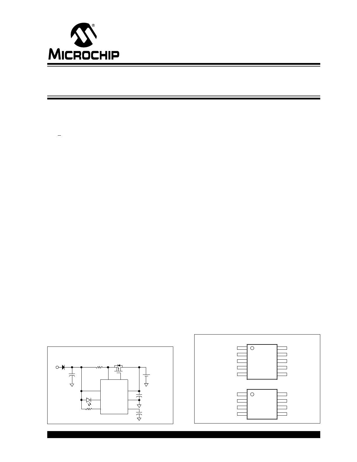
Typical Application Circuit
Description
The MCP7384X family of devices are highly advanced
linear charge management controllers for use in
space-limited, cost-sensitive applications. The
MCP73841 and MCP73842 combine high accuracy,
constant-voltage, constant-current regulation, cell pre-
conditioning, cell temperature monitoring, advanced
safety timers, automatic charge termination and
charge status indication in space-saving, 10-pin
MSOP packages. The MCP73841 and MCP73842
provide complete, fully-functional, stand-alone charge
management solutions.
The MCP73843 and MCP73844 employ all the
features of the MCP73841 and MCP73842, with the
exception of the cell temperature monitor. The
MCP73843 and MCP73844 are offered in 8-pin MSOP
packages.
The MCP73841 and MCP73843 are designed for
applications utilizing single-cell Lithium-Ion or Lithium-
Polymer battery packs. Two preset voltage regulation
options are available (4.1V and 4.2V) for use with either
coke or graphite anodes. The MCP73841 and
MCP73843 operate with an input voltage range of 4.5V
to 12V.
The MCP73842 and MCP73844 are designed for
applications utilizing dual series cell Lithium-Ion or
Lithium-Polymer battery packs. Two preset voltage
regulation options are available (8.2V and 8.4V). The
MCP73842 and MCP73844 operate with an input
voltage range of 8.7V to 12V.
The MCP7384X family of devices are fully specified
over the ambient temperature range of -40°C to +85°C.
Package Types
+
-
V
SS
DRV
SENSE
V
DD
V
BAT
STAT1
3
6
7
1
2
MCP73843
8
10 µF
10 µF
100 k
100 m
5V
Single
Lithium-Ion
Cell
NDS8434
MA2Q705
1A Lithium-Ion Battery Charger
EN
5
TIMER
4
0.1 µF
10-Pin MSOP
SENSE
V
DD
STAT1
EN
DRV
V
BAT
V
SS
TIMER
1
2
3
4
8
7
6
5
M
C
P73
843
M
C
P73
844
8-Pin MSOP
V
DD
STAT1
EN
THREF
V
BAT
V
SS
TIMER
THERM
2
3
4
5
9
8
7
6
M
C
P73
841
M
C
P73
842
SENSE
DRV
1
10
Advanced Single or Dual Cell Lithium-Ion/
Lithium-Polymer Charge Management Controllers
MCP73841/2/3/4
DS21823D-page 2
2003-2013 Microchip Technology Inc.
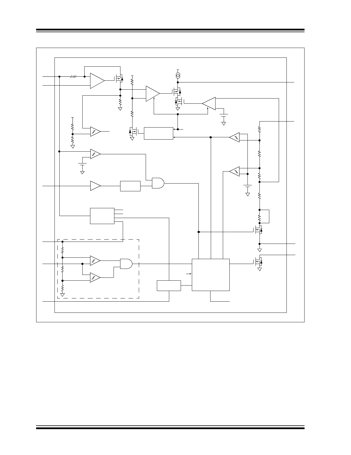
Functional Block Diagram
Charge
Termination
Comparator
Voltage Control
Amplifier
V
REF
I
REG
/10
Precondition
Control
Charge_ok
Precon
V
DD
Charge Current
Control Amplifier
+
–
V
REF
V
REF
Precondition
Comp.
V
BAT
V
SS
DRV
90 k
90 k
10 k
10 k
+
–
Charge
Current
Amplifier
V
DD
SENSE
MCP73841 and MCP73842 Only
300 k
(825 k
)
12 k
1 k
UVLO
Comparator
V
UVLO
Temperature
Comparators
Bias and
Reference
Generator
V
UVLO
V
REF
(1.2V)
Power-On
Delay
V
REF
Oscillator
Constant-Voltage/
Recharge Comp.
Charge Control,
Charge Timers,
And
Status Logic
Drv Stat 1
Charge_ok
I
REG
/10
THERM
EN
TIMER
STAT1
THREF
100 k
50 k
50 k
74.21 k
0.79 k
150.02 k
5.15 k
(4.29 k
)
+
-
+
-
+
-
+
-
+
-
+
-
+
-
2003-2013 Microchip Technology Inc.
DS21823D-page 3
MCP73841/2/3/4
1.0
ELECTRICAL
CHARACTERISTICS
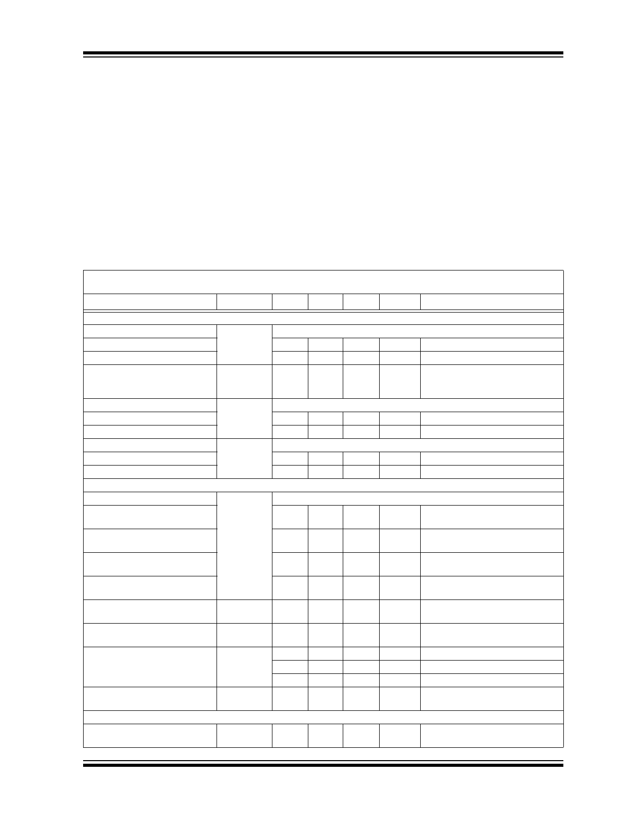
Absolute Maximum Ratings †
V
DD
.................................................................................13.5V
All inputs and outputs w.r.t. V
SS
................ -0.3 to (V
DD
+0.3)V
Current at DRV Pin ......................................................±4 mA
Current at STAT1 Pin .................................................±30 mA
Maximum Junction Temperature, T
J
............................. 150°C
Storage temperature .....................................-65°C to +150°C
ESD protection on all pins:
Human Body Model (1.5 k
in Series with 100 pF)2 kV
Machine Model (200 pF, No Series Resistance) .............200V
*Notice: Stresses above those listed under “Maximum
Ratings” may cause permanent damage to the device. This is
a stress rating only and functional operation of the device at
those or any other conditions above those indicated in the
operational listings of this specification is not implied. Expo-
sure to maximum rating conditions for extended periods may
affect device reliability.
DC CHARACTERISTICS
Electrical Specifications: Unless otherwise indicated, all limits apply for V
DD
= [V
REG
(Typ)+0.3V] to 12V, T
A
= -40°C to +85°C.
Typical values are at +25°C, V
DD
= [V
REG
(Typ) + 1V].
Parameters
Sym
Min
Typ
Max
Units
Conditions
Supply Input
Supply Voltage
V
DD
MCP73841, MCP73843
4.5
–
12
V
MCP73842, MCP73844
8.7
–
12
V
Supply Current
I
SS
–
–
0.25
0.75
4
4
µA
mA
Disabled
Operating
V
DD
=V
REG
(Typ)+1V
UVLO Start Threshold
V
START
MCP73841, MCP73843
4.25
4.45
4.60
V
V
DD
Low-to-High
MCP73842, MCP73844
8.45
8.65
8.90
V
V
DD
Low-to-High
UVLO Stop Threshold
V
STOP
MCP73841, MCP73843
4.20
4.40
4.55
V
V
DD
High-to-Low
MCP73842, MCP73844
8.40
8.60
8.85
V
V
DD
High-to-Low
Voltage Regulation (Constant-Voltage Mode)
Regulated Output Voltage
V
REG
MCP73841-4.1,
MCP73843-4.1
4.079
4.1
4.121
V
V
DD
= [V
REG
(Typ)+1V], I
OUT
= 10 mA,
T
A
= -5°C to +55°C
MCP73841-4.2,
MCP73843-4.2
4.179
4.2
4.221
V
V
DD
= [V
REG
(Typ)+1V], I
OUT
= 10 mA,
T
A
= -5°C to +55°C
MCP73842-8.2,
MCP73844-8.2
8.159
8.2
8.241
V
V
DD
= [V
REG
(Typ)+1V], I
OUT
= 10 mA,
T
A
= -5°C to +55°C
MCP73842-8.4,
MCP73844-8.4
8.358
8.4
8.442
V
V
DD
= [V
REG
(Typ)+1V], I
OUT
= 10 mA,
T
A
= -5°C to +55°C
Line Regulation
V
BAT
/
V
BAT
)|/
V
DD
–
0.025
0.25
%/V
V
DD
= [V
REG
(Typ)+1V] to 12V,
I
OUT
= 10 mA
Load Regulation
V
BAT
|/V
BAT
–
0.01
0.25
%
I
OUT
= 10 mA to 150 mA,
V
DD
= [V
REG
(Typ)+1V]
Supply Ripple Attenuation
PSRR
–
-58
–
dB
I
OUT
= 10 mA, 100 Hz
–
-42
–
dB
I
OUT
= 10 mA, 1 kHz
–
-30
–
dB
I
OUT
= 10 mA, 10 kHz
Output Reverse Leakage
Current
I
DISCHARGE
–
0.4
1
µA
V
DD
Floating, V
BAT
= V
REG
(Typ)
Current Regulation (Fast Charge Constant-Current Mode)
Fast Charge Current
Regulation Threshold
V
FCS
100
110
120
mV
V
DD
– V
SENSE,
T
A
= -5°C to +55°C
MCP73841/2/3/4
DS21823D-page 4
2003-2013 Microchip Technology Inc.
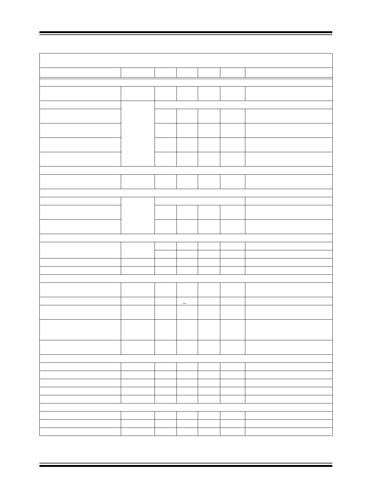
Preconditioning Current Regulation (Trickle Charge Constant-Current Mode)
Precondition Current
Regulation Threshold
V
PCS
5
10
15
mV
V
DD
– V
SENSE,
T
A
= -5°C to +55°C
Precondition Threshold Voltage
V
PTH
MCP73841-4.1,
MCP73843-4.1
2.70
2.80
2.90
V
V
BAT
Low-to-High
MCP73841-4.2,
MCP73843-4.2
2.75
2.85
2.95
V
V
BAT
Low-to-High
MCP73842-8.2,
MCP73844-8.2
5.40
5.60
5.80
V
V
BAT
Low-to-High
MCP73842-8.4,
MCP73844-8.4
5.50
5.70
5.90
V
V
BAT
Low-to-High
Charge Termination
Charge Termination Threshold
V
TCS
4
7
10
mV
V
DD
– V
SENSE,
T
A
= -5°C to +55°C
Automatic Recharge
Recharge Threshold Voltage
V
RTH
MCP73841,
MCP73843
V
REG
-
300 mV
V
REG
-
200 mV
V
REG
-
100 mV
V
V
BAT
High-to-Low
MCP73842,
MCP73844
V
REG
-
600 mV
V
REG
-
400 mV
V
REG
-
200 mV
V
V
BAT
High-to-Low
External MOSFET Gate Drive
Gate Drive Current
I
DRV
–
2
–
mA
Sink, CV Mode
–
-0.5
–
mA
Source, CV Mode
Gate Drive Minimum Voltage
V
DRVMIN
–
–
1.0
V
V
DD
= 4.5V
Gate - Source Clamp Voltage
V
GS
-7.0
–
-4.5
V
V
DD
= 12.0V
Thermistor Reference - MCP73841, MCP73842
Thermistor Reference Output
Voltage
V
THREF
2.475
2.55
2.625
V
T
A
= +25°C, V
DD
= V
REG
(Typ)+1V,
I
THREF
= 0 mA
Temperature Coefficient
TC
THREF
–
+50
–
ppm/°C
Thermistor Reference Source
Current
I
THREF
200
–
–
µA
Thermistor Reference Line
Regulation
V
THREF
/
V
THREF
)|/
V
DD
–
0.1
0.25
%/V
V
DD
=[V
REG
(Typ)+1V] to 12V
Thermistor Reference Load
Regulation
V
THREF
/
V
THREF
–
0.01
0.10
%
I
THREF
= 0 mA to 0.20 mA
Thermistor Comparator - MCP73841, MCP73842
Upper Trip Threshold
V
T1
1.18
1.25
1.32
V
Upper Trip Point Hysteresis
V
T1HYS
–
-50
–
mV
Lower Trip Threshold
V
T2
0.59
0.62
0.66
V
Lower Trip Point Hysteresis
V
T2HYS
–
80
–
mV
Input Bias Current
|I
BIAS
|
–
–
2
µA
Status Indicator
Sink Current
I
SINK
4
7
12
mA
Low Output Voltage
V
OL
–
200
400
mV
I
SINK
= 1 mA
Input Leakage Current
I
LK
–
0.01
1
µA
I
SINK
= 0 mA, V
STAT1
= 12V
DC CHARACTERISTICS (CONTINUED)
Electrical Specifications: Unless otherwise indicated, all limits apply for V
DD
= [V
REG
(Typ)+0.3V] to 12V, T
A
= -40°C to +85°C.
Typical values are at +25°C, V
DD
= [V
REG
(Typ) + 1V].
Parameters
Sym
Min
Typ
Max
Units
Conditions
2003-2013 Microchip Technology Inc.
DS21823D-page 5
MCP73841/2/3/4
AC CHARACTERISTICS
TEMPERATURE SPECIFICATIONS
Enable Input
Input High-Voltage Level
V
IH
1.4
-
–
V
Input Low-Voltage Level
V
IL
–
-
0.8
V
Input Leakage Current
I
LK
–
0.01
1
µA
V
ENABLE
= 12V
Electrical Specifications: Unless otherwise indicated, all limits apply for V
DD
= [V
REG
(Typ)+0.3V] to 12V, T
A
= -40°C to +85°C. Typ-
ical values are at +25°C, V
DD
= [V
REG
(Typ)+1V].
Parameters
Sym
Min
Typ
Max
Units
Conditions
UVLO Start Delay
t
START
–
–
5
msec
V
DD
Low-to-High
Current Regulation
Transition Time Out of
Preconditioning
t
DELAY
–
–
1
msec
V
BAT
< V
PTH
to V
BAT
> V
PTH
Current Rise Time Out of
Preconditioning
t
RISE
–
–
1
msec
I
OUT
Rising to 90% of I
REG
Fast Charge Safety Timer Period
t
FAST
1.1
1.5
1.9
Hours
C
TIMER
= 0.1 µF
Preconditioning Current Regulation
Preconditioning Charge Safety
Timer Period
t
PRECON
45
60
75
Minutes
C
TIMER
= 0.1 µF
Charge Termination
Elapsed Time Termination Period
t
TERM
2.2
3.0
3.8
Hours
C
TIMER
= 0.1 µF
Status Indicators
Status Output turn-off
t
OFF
–
–
200
µsec
I
SINK
= 10 mA to 0 mA
Status Output turn-on
t
ON
–
–
200
µsec
I
SINK
= 0 mA to 10 mA
Electrical Specifications: Unless otherwise specified, all limits apply for V
DD
= [V
REG
(Typ)+0.3V] to 12V.
Typical values are at +25°C, V
DD
= [V
REG
(Typ)+1.0V].
Parameters
Sym
Min
Typ
Max
Units
Conditions
Temperature Ranges
Specified Temperature Range
T
A
-40
+85
°C
Operating Temperature Range
T
A
-40
+125
°C
Storage Temperature Range
T
A
-65
+150
°C
Thermal Package Resistances
Thermal Resistance, MSOP-10
JA
113
°C/W
4-Layer JC51-7 Standard Board,
Natural Convection
Thermal Resistance, MSOP-8
JA
206
°C/W
Single-Layer SEMI G42-88 Board,
Natural Convection
DC CHARACTERISTICS (CONTINUED)
Electrical Specifications: Unless otherwise indicated, all limits apply for V
DD
= [V
REG
(Typ)+0.3V] to 12V, T
A
= -40°C to +85°C.
Typical values are at +25°C, V
DD
= [V
REG
(Typ) + 1V].
Parameters
Sym
Min
Typ
Max
Units
Conditions
MCP73841/2/3/4
DS21823D-page 6
2003-2013 Microchip Technology Inc.
2.0
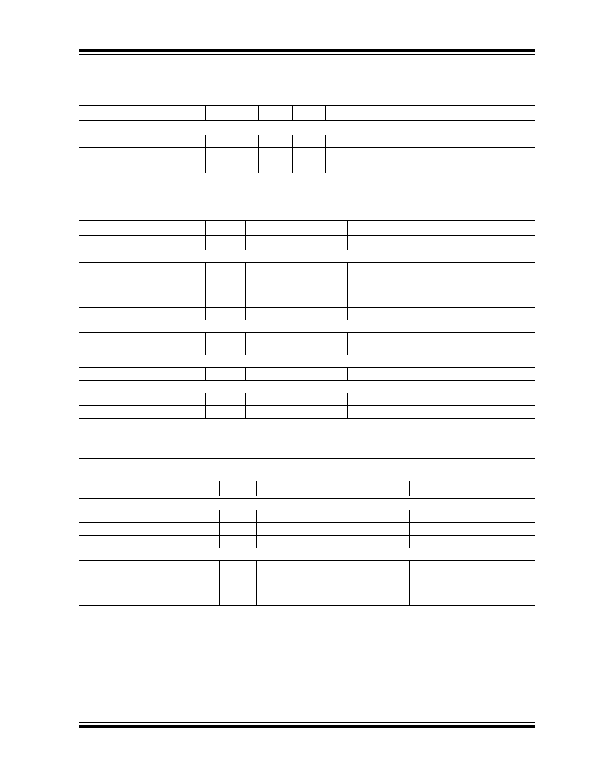
TYPICAL PERFORMANCE CURVES
Note: Unless otherwise indicated, V
DD
= [V
REG
(Typ) + 1V], I
OUT
= 10 mA and T
A
= +25°C.
FIGURE 2-1:
Battery Regulation Voltage
(V
BAT
) vs. Charge Current (I
OUT
).
FIGURE 2-2:
Battery Regulation Voltage
(V
BAT
) vs. Supply Voltage (V
DD
).
FIGURE 2-3:
Battery Regulation Voltage
(V
BAT
) vs. Supply Voltage (V
DD
).
FIGURE 2-4:
Supply Current (I
SS
) vs.
Charge Current (I
OUT
).
FIGURE 2-5:
Supply Current (I
SS
) vs.
Supply Voltage (V
DD
).
FIGURE 2-6:
Supply Current (I
SS
) vs.
Supply Voltage (V
DD
).
Note:
The graphs and tables provided following this note are a statistical summary based on a limited number of
samples and are provided for informational purposes only. The performance characteristics listed herein
are not tested or guaranteed. In some graphs or tables, the data presented may be outside the specified
operating range (e.g., outside specified power supply range) and therefore outside the warranted range.
4.196
4.197
4.198
4.199
4.200
4.201
4.202
4.203
10
100
1000
I
OUT
(mA)
V
BA
T
(V
)
+55°C
+25°C
-5°C
MCP73841-4.2V
V
DD
= 5.2 V
4.196
4.197
4.198
4.199
4.200
4.201
4.202
4.203
4.5
6.0
7.5
9.0
10.5
12.0
V
DD
(V)
V
BAT
(V
)
+55°C
+25°C
-5°C
MCP73841-4.2V
I
OUT
= 1000 mA
4.196
4.197
4.198
4.199
4.200
4.201
4.202
4.203
4.5
6.0
7.5
9.0
10.5
12.0
V
DD
(V)
V
BAT
(V
)
MCP73841-4.2V
I
OUT
= 10 mA
+55°C
+25°C
-5°C
0.00
0.20
0.40
0.60
0.80
1.00
1.20
1.40
10
100
1000
I
OUT
(mA)
I
SS
(m
A
)
+25°C
+85°C
-45°C
MCP73841-4.2V
V
DD
= 5.2 V
0.00
0.20
0.40
0.60
0.80
1.00
1.20
1.40
4.5
6.0
7.5
9.0
10.5
12.0
V
DD
(V)
I
SS
(m
A
)
+25°C
+85°C
-45°C
MCP73841-4.2V
I
OUT
= 1000 mA
0.00
0.20
0.40
0.60
0.80
1.00
1.20
1.40
4.5
6.0
7.5
9.0
10.5
12.0
V
DD
(V)
I
SS
(m
A
)
MCP73841-4.2V
I
OUT
= 10 mA
-45°C
+25°C
+85°C
2003-2013 Microchip Technology Inc.
DS21823D-page 7
MCP73841/2/3/4
Note: Unless otherwise indicated, V
DD
= [V
REG
(Typ) + 1V], I
OUT
= 10 mA and T
A
= +25°C.
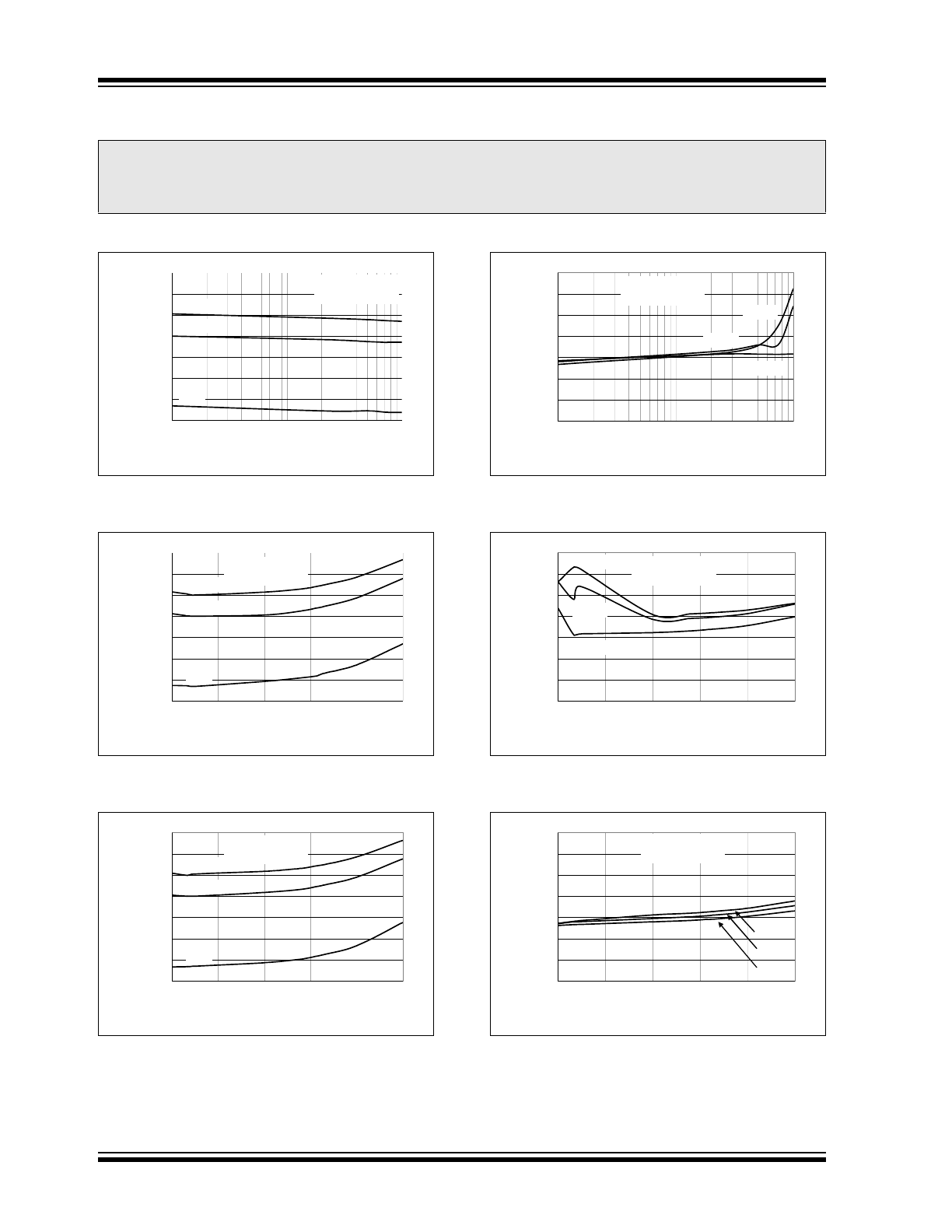
FIGURE 2-7:
Battery Regulation Voltage
(V
BAT
) vs. Charge Current (I
OUT
).
FIGURE 2-8:
Battery Regulation Voltage
(V
BAT
) vs. Supply Voltage (V
DD
).
FIGURE 2-9:
Battery Regulation Voltage
(V
BAT
) vs. Supply Voltage (V
DD
).
FIGURE 2-10:
Supply Current (I
SS
) vs.
Charge Current (I
OUT
).
FIGURE 2-11:
Supply Current (I
SS
) vs.
Supply Voltage (V
DD
).
FIGURE 2-12:
Supply Current (I
SS
) vs.
Supply Voltage (V
DD
).
8.390
8.392
8.394
8.396
8.398
8.400
8.402
8.404
8.406
8.408
10
100
1000
I
OUT
(mA)
V
BAT
(V
)
+55°C
+25°C
-5°C
MCP73842-8.4V
V
DD
= 9.4 V
8.390
8.392
8.394
8.396
8.398
8.400
8.402
8.404
8.406
8.408
8.8
9.2
9.6
10
10.4 10.8 11.2 11.6
12
V
DD
(V)
V
BAT
(V
)
+55°C
+25°C
-5°C
MCP73842-8.4V
I
OUT
= 1000 mA
8.390
8.392
8.394
8.396
8.398
8.400
8.402
8.404
8.406
8.408
8.8
9.2
9.6
10.0 10.4 10.8 11.2 11.6 12.0
V
DD
(V)
V
BAT
(V
)
MCP73842-8.4V
I
OUT
= 10 mA
+55°C
+25°C
-5°C
0.00
0.20
0.40
0.60
0.80
1.00
1.20
1.40
10
100
1000
I
OUT
(mA)
I
SS
(m
A
)
+25°C
+85°C
-45°C
MCP73842-8.4V
V
DD
= 9.4 V
0.00
0.20
0.40
0.60
0.80
1.00
1.20
1.40
8.8
9.2
9.6
10.0 10.4 10.8 11.2 11.6 12.0
V
DD
(V)
I
SS
(m
A
)
+25°C
+85°C
-45°C
MCP73842-8.4V
I
OUT
= 1000 mA
0.00
0.20
0.40
0.60
0.80
1.00
1.20
1.40
8.8
9.2
9.6
10.0 10.4 10.8 11.2 11.6 12.0
V
DD
(V)
I
SS
(m
A
)
MCP73842-8.4V
I
OUT
= 10 mA
-45°C
+25°C
+85°C
MCP73841/2/3/4
DS21823D-page 8
2003-2013 Microchip Technology Inc.
Note: Unless otherwise indicated, V
DD
= [V
REG
(Typ) + 1V], I
OUT
= 10 mA and T
A
= +25°C.
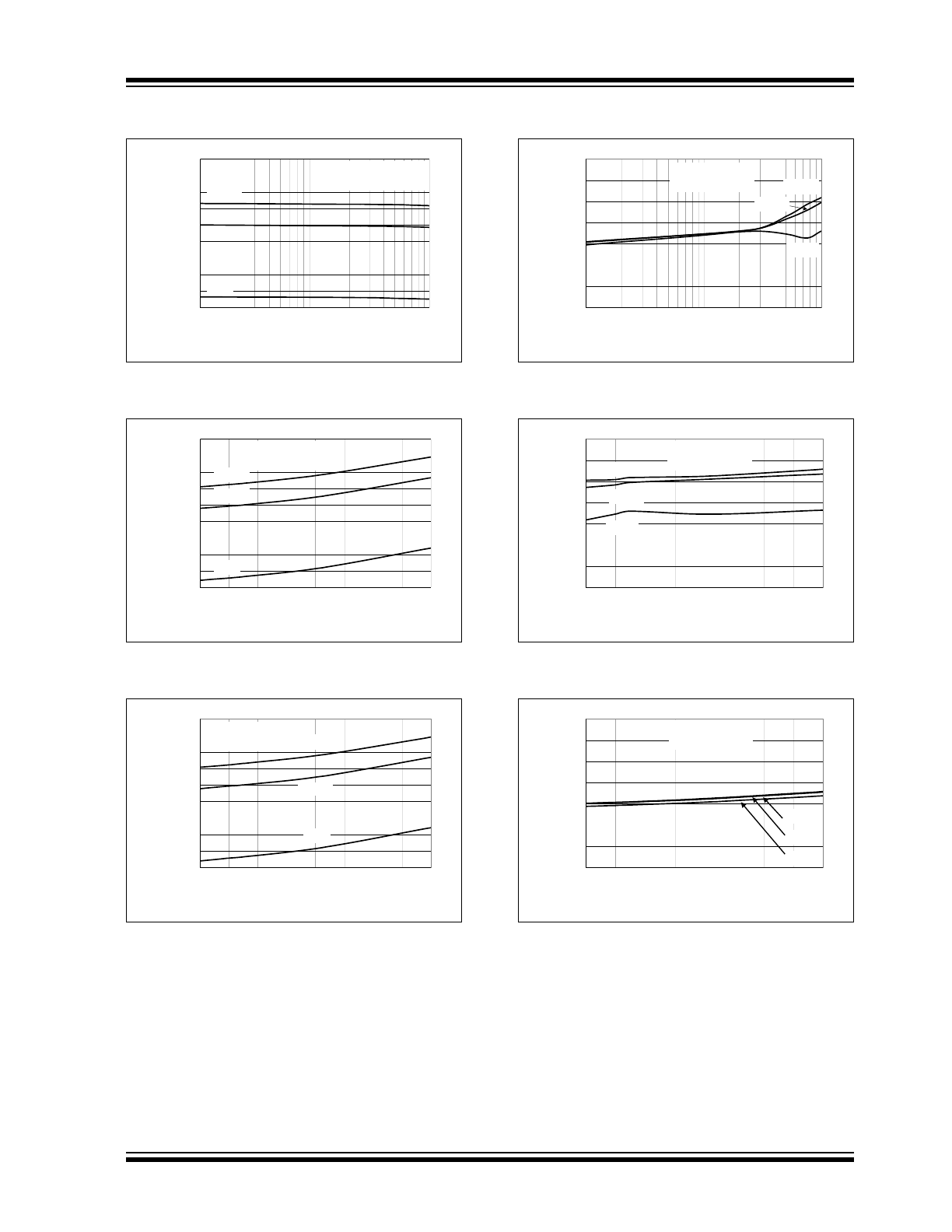
FIGURE 2-13:
Output Reverse Leakage
Current (I
DISCHARGE
) vs. Battery Voltage (V
BAT
).
FIGURE 2-14:
Thermistor Reference
Voltage (V
THREF
) vs. Thermistor Bias Current
(I
THREF
).
FIGURE 2-15:
Thermistor Reference
Voltage (V
THREF
) vs. Supply Voltage (V
DD
).
FIGURE 2-16:
Output Reverse Leakage
Current (I
DISCHARGE
) vs. Battery Voltage (V
BAT
).
FIGURE 2-17:
Thermistor Reference
Voltage (V
THREF
) vs. Thermistor Bias Current
(I
THREF
).
FIGURE 2-18:
Thermistor Reference
Voltage (V
THREF
) vs. Supply Voltage (V
DD
).
0.00
0.05
0.10
0.15
0.20
0.25
0.30
0.35
0.40
0.45
2.0 2.2 2.4 2.6 2.8 3.0 3.2 3.4 3.6 3.8 4.0 4.2
V
BAT
(V)
I
DISCHARGE
(µA
)
+25°C
+85°C
-45°C
MCP73841-4.2V
V
DD
= Float
2.540
2.542
2.544
2.546
2.548
2.550
2.552
2.554
2.556
2.558
2.560
0
25
50
75
100
125
150
175
200
I
THREF
(µA)
V
T
HREF
(V
)
+85°C
+25°C
-45°C
MCP73841-4.2V
V
DD
= 5.2 V
2.540
2.544
2.548
2.552
2.556
2.560
2.564
2.568
4.5
6.0
7.5
9.0
10.5
12.0
V
DD
(V)
V
T
HREF
(V
)
+85°C
+25°C
-45°C
MCP73841-4.2V
I
THREF
= 100 µA
0.00
0.10
0.20
0.30
0.40
0.50
0.60
0.70
0.80
0.90
4.0 4.4 4.8 5.2 5.6 6.0 6.4 6.8 7.2 7.6 8.0 8.4
V
BAT
(V)
I
DISCHARGE
(µA
)
MCP73842-8.4V
V
DD
= Float
-45°C
+25°C
+85°C
2.540
2.542
2.544
2.546
2.548
2.550
2.552
2.554
2.556
2.558
2.560
0
25
50
75
100
125
150
175
200
I
THREF
(µA)
V
T
HREF
(V
)
+25°C
+85°C
-45°C
MCP73842-8.4V
V
DD
= 9.4 V
2.540
2.544
2.548
2.552
2.556
2.560
2.564
2.568
8.8
9.2
9.6
10.0 10.4 10.8 11.2 11.6 12.0
V
DD
(V)
V
T
HREF
(V
)
MCP73842-8.4V
I
THREF
= 100 µA
+85°C
+25°C
-45°C
2003-2013 Microchip Technology Inc.
DS21823D-page 9
MCP73841/2/3/4
Note: Unless otherwise indicated, V
DD
= [V
REG
(Typ) + 1V], I
OUT
= 10 mA and T
A
= +25°C.
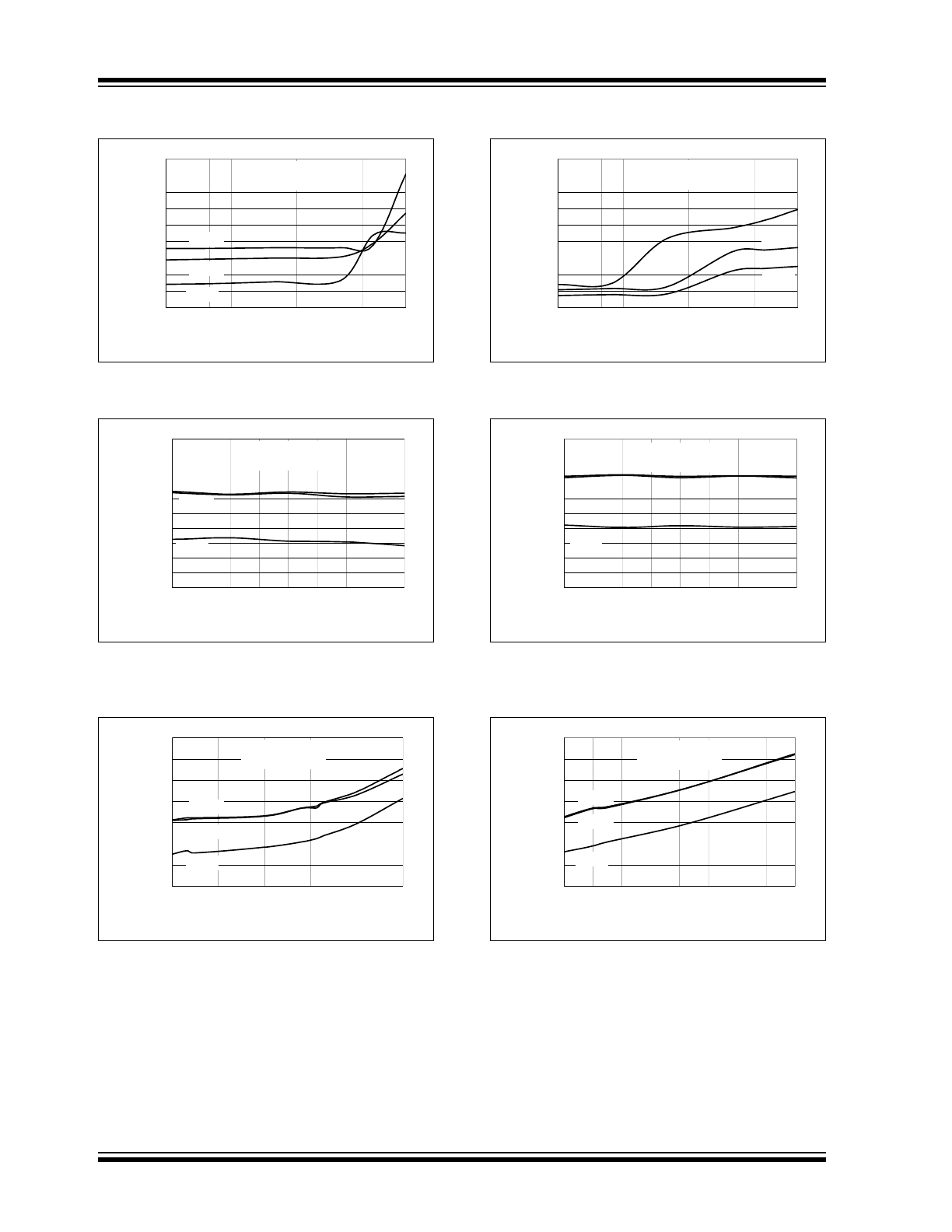
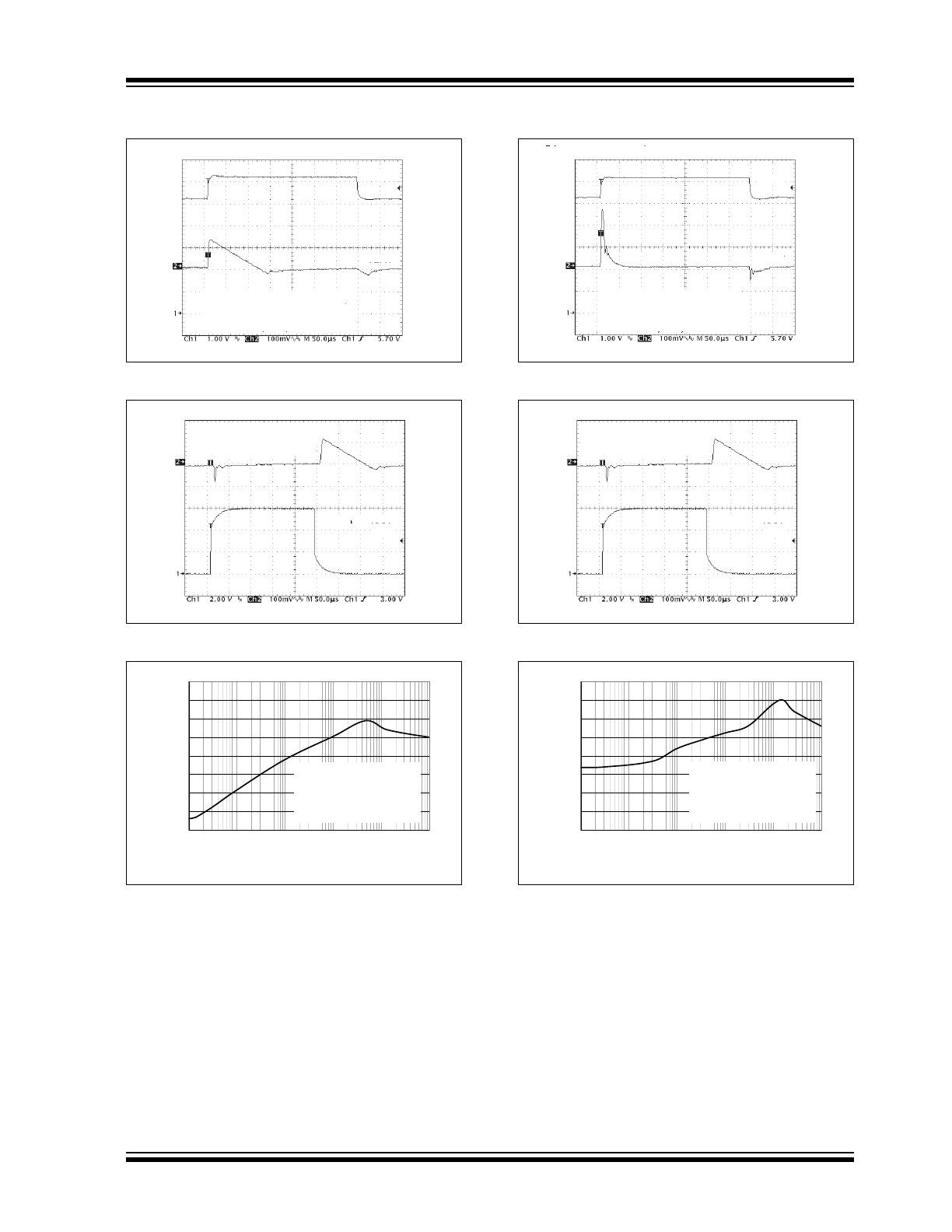
FIGURE 2-19:
Line Transient Response.
FIGURE 2-20:
Load Transient Response.
FIGURE 2-21:
Power Supply Ripple
Rejection.
FIGURE 2-22:
Line Transient Response.
FIGURE 2-23:
Load Transient Response.
FIGURE 2-24:
Power Supply Ripple
Rejection.
V
DD
V
BAT
MCP73841-4.2V
V
DD
Stepped From 5.2V to 6.2V
I
OUT
= 10 mA
C
OUT
= 10 µF, X7R, Ceramic
MCP73841-4.2V
V
DD
= 5.2V
C
OUT
= 10 µF, X7R, Ceramic
V
BAT
I
OUT
100 mA
10 mA
-80
-70
-60
-50
-40
-30
-20
-10
0
0.01
0.1
1
10
100
1000
Frequency (kHz)
A
ttenuation (dB
)
MCP73841-4.2V
V
DD
= 5.2 V
V
AC
= 100 mVp-p
I
OUT
= 10 mA
C
OUT
= 10 µF, X7R, CERAMIC
V
DD
V
BAT
MCP73841-4.2V
V
DD
Stepped From 5.2V to 6.2V
I
OUT
= 500 mA
C
OUT
= 10 µF, X7R, Ceramic
V
BAT
MCP73841-4.2V
V
DD
= 5.2V
C
OUT
= 10 µF, X7R, Ceramic
I
OUT
500 mA
10 mA
-80
-70
-60
-50
-40
-30
-20
-10
0
0.01
0.1
1
10
100
1000
Frequency (kHz)
A
ttenuation (dB
)
MCP73841-4.2V
V
DD
= 5.2 V
V
AC
= 100 mVp-p
I
OUT
= 100 mA
C
OUT
= 10 µF, X7R, CERAMIC
MCP73841/2/3/4
DS21823D-page 10
2003-2013 Microchip Technology Inc.
3.0
PIN DESCRIPTIONS
The descriptions of the pins are listed in Table 3-1.
TABLE 3-1:
PIN DESCRIPTION TABLE
3.1
Charge Current Sense Input
(SENSE)
Charge current is sensed via the voltage developed
across an external precision sense resistor. The sense
resistor must be placed between the supply voltage
(V
DD
) and the external pass transistor (Q1). A 220 m
sense resistor produces a fast charge current of
500 mA, typically.
3.2
Battery Management Input Supply
(V
DD
)
A supply voltage of [V
REG
(Typ) + 0.3V] to 12V is
recommended. Bypass to V
SS
with a minimum of
4.7 µF.
3.3
Charge Status Output (STAT1)
Current limited, open-drain drive for direct connection
to a LED for charge status indication. Alternatively, a
pull-up resistor can be applied for interfacing to a host
microcontroller.
3.4
Logic Enable (EN)
Input to force charge termination, initiate charge, clear
faults or disable automatic recharge.
3.5
Cell Temperature Sensor Bias
(THREF)
Voltage reference to bias external thermistor for
continuous cell temperature monitoring and
prequalification.
3.6
Cell Temperature Sensor Input
(THERM)
Input for an external thermistor for continuous cell-
temperature monitoring and pre-qualification. Apply a
voltage equal to 0.85V to disable temperature-sensing.
3.7
Timer Set (TIMER)
All safety timers are scaled by C
TIMER
/0.1 µF.
3.8
Battery Management 0V Reference
(V
SS
)
Connect to negative terminal of battery.
3.9
Battery Voltage Sense (V
BAT
)
Voltage sense input. Connect to positive terminal of
battery. Bypass to V
SS
with a minimum of 4.7 µF to
ensure loop stability when the battery is disconnected.
A precision internal resistor divider regulates the final
voltage on this pin to V
REG
.
3.10
Drive Output (DRV)
Direct output drive of an external P-channel MOSFET
for current and voltage regulation.
MCP73841,
MCP73842
Pin No.
MCP73843,
MCP73844
Pin No.
Name
Function
1
1
SENSE
Charge Current Sense Input
2
2
V
DD
Battery Management Input Supply
3
3
STAT1
Charge Status Output
4
4
EN
Logic Enable
5
—
THREF
Cell Temperature Sensor Bias
6
—
THERM
Cell Temperature Sensor Input
7
5
TIMER
Timer Set
8
6
V
SS
Battery Management 0V Reference
9
7
V
BAT
Battery Voltage Sense
10
8
DRV
Drive Output