
©
2007 Microchip Technology Inc.
DS21808D-page 1
25AA080A/B, 25LC080A/B
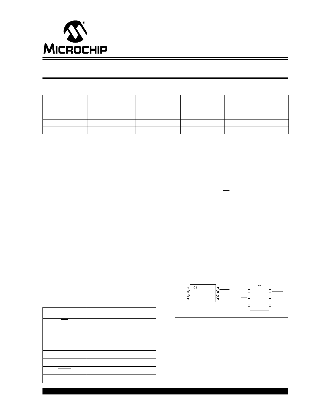
Device Selection Table
Features
• Max. clock 10 MHz
• Low-power CMOS technology
• 1024 x 8-bit organization
• 16 byte page (‘A’ version devices)
• 32 byte page (‘B’ version devices)
• Write cycle time: 5 ms max.
• Self-timed ERASE and WRITE cycles
• Block write protection
- Protect none, 1/4, 1/2 or all of array
• Built-in write protection
- Power-on/off data protection circuitry
- Write enable latch
- Write-protect pin
• Sequential read
• High reliability
- Endurance: 1,000,000 erase/write cycles
- Data retention: > 200 years
- ESD protection: > 4000V
• Pb-free and RoHS compliant
• Temperature ranges supported;
Pin Function Table
Description
The Microchip Technology Inc. 25AA080A/B,
25LC080A/B (25XX080A/B
*
) are 8 Kbit Serial
Electrically Erasable PROMs. The memory is accessed
via a simple Serial Peripheral Interface (SPI)
compatible serial bus. The bus signals required are a
clock input (SCK) plus separate data in (SI) and data
out (SO) lines. Access to the device is controlled
through a Chip Select (CS) input.
Communication to the device can be paused via the
hold pin (HOLD). While the device is paused, transi-
tions on its inputs will be ignored, with the exception of
chip select, allowing the host to service higher priority
interrupts.
The 25XX080A/B is available in standard packages
including 8-lead PDIP and SOIC, and advanced
packaging including 8-lead MSOP, and 8-lead TSSOP.
All packages are Pb-free and RoHS compliant.
Package Types (not to scale)
Part Number
V
CC
Range
Page Size
Temp. Ranges
Packages
25LC080A
2.5-5.5V
16 Byte
I, E
P, SN, ST, MS
25AA080A
1.8-5.5V
16 Byte
I
P, SN, ST, MS
25LC080B
2.5-5.5V
32 Byte
I, E
P, SN, ST, MS
25AA080B
1.8-5.5V
32 Byte
I
P, SN, ST, MS
- Industrial (I):
-40
°
C to
+85
°
C
- Automotive (E):
-40°C to +125°C
Name
Function
CS
Chip Select Input
SO
Serial Data Output
WP
Write-Protect
V
SS
Ground
SI
Serial Data Input
SCK
Serial Clock Input
HOLD
Hold Input
V
CC
Supply Voltage
CS
SO
WP
V
SS
1
2
3
4
8
7
6
5
V
CC
HOLD
SCK
SI
PDIP/SOIC
(P, SN)
TSSOP/MSOP
CS
SO
WP
V
SS
1
2
3
4
8
7
6
5
V
CC
HOLD
SCK
SI
(ST, MS)
8K SPI Bus Serial EEPROM
*25XX080A/B is used in this document as a generic part
number for the 25AA080A/B, 25LC080A/B.
25XX080A/B
DS21808D-page 2
©
2007 Microchip Technology Inc.
1.0
ELECTRICAL CHARACTERISTICS
Absolute Maximum Ratings
(†)
V
CC
.............................................................................................................................................................................7.0V
All inputs and outputs w.r.t. V
SS
......................................................................................................... -0.6V to V
CC
+1.0V
Storage temperature .................................................................................................................................-65°C to 150°C
Ambient temperature under bias ...............................................................................................................-65°C to 125°C
ESD protection on all pins .......................................................................................................................................... 4 kV
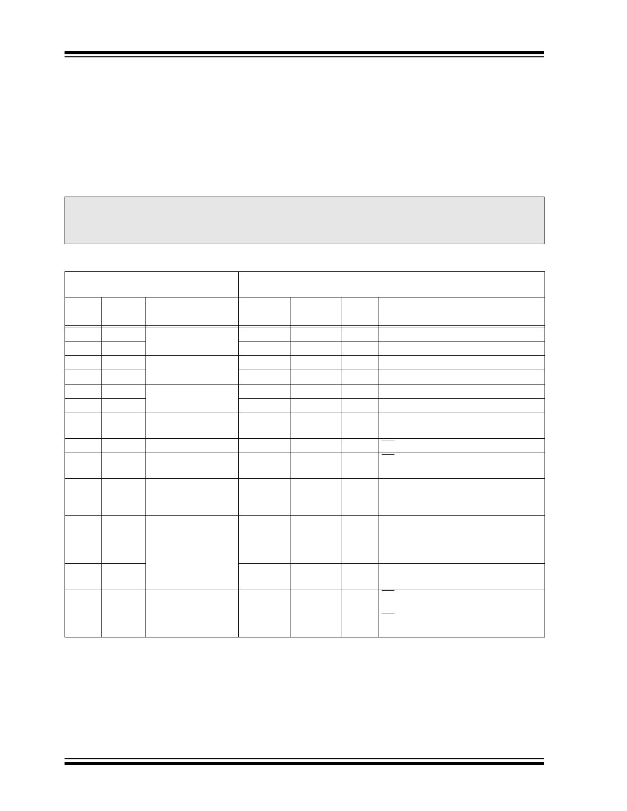
TABLE 1-1:
DC CHARACTERISTICS
† NOTICE: Stresses above those listed under “Absolute Maximum Ratings” may cause permanent damage to the
device. This is a stress rating only and functional operation of the device at those or any other conditions above those
indicated in the operational listings of this specification is not implied. Exposure to maximum rating conditions for an
extended period of time may affect device reliability.
DC CHARACTERISTICS
Industrial (I):
T
AMB
= -40°C to +85°C
V
CC
= 1.8V to 5.5V
Automotive (E): T
AMB
= -40°C to +125°C
V
CC
= 2.5V to 5.5V
Param.
No.
Sym.
Characteristic
Min.
Max.
Units
Test Conditions
D001
V
IH
1
High-level input
voltage
2.0
V
CC
+1
V
V
CC
≥
2.7V (Note)
D002
V
IH
2
0.7 V
CC
V
CC
+1
V
V
CC
< 2.7V (Note)
D003
V
IL
1
Low-level input
voltage
-0.3
0.8
V
V
CC
≥
2.7V (Note)
D004
V
IL
2
-0.3
0.2 V
CC
V
V
CC
< 2.7V (Note)
D005
V
OL
Low-level output
voltage
—
0.4
V
I
OL
= 2.1 mA
D006
V
OL
—
0.2
V
I
OL
= 1.0 mA, V
CC
< 2.5V
D007
V
OH
High-level output
voltage
V
CC
-0.5
—
V
I
OH
= -400
μ
A
D008
I
LI
Input leakage current
±1
μ
A
CS = V
CC
, V
IN
= V
SS
TO
V
CC
D009
I
LO
Output leakage
current
±1
μ
A
CS = V
CC
, V
OUT
= V
SS
TO
V
CC
D010
C
INT
Internal Capacitance
(all inputs and
outputs)
—
7
pF
T
AMB
= 25°C, CLK = 1.0 MHz,
V
CC
= 5.0V (Note)
D011
I
CC
Read
Operating Current
—
—
6
2.5
mA
mA
V
CC
= 5.5V; F
CLK
= 10.0 MHz;
SO = Open
V
CC
= 2.5V; F
CLK
= 5.0 MHz;
SO = Open
D012
I
CC
Write
—
—
3
mA
V
CC
= 5.5V
D013
Iccs
Standby Current
—
—
5
1
μ
A
μ
A
CS = V
CC
= 5.5V, Inputs tied to V
CC
or
V
SS
, T
AMB
= -40°C
TO
+125°C
CS = V
CC
= 2.5V, Inputs tied to V
CC
or
V
SS
, T
AMB
= -40°C
TO
+85°C
Note:
This parameter is periodically sampled and not 100% tested.
©
2007 Microchip Technology Inc.
DS21808D-page 3
25XX080A/B
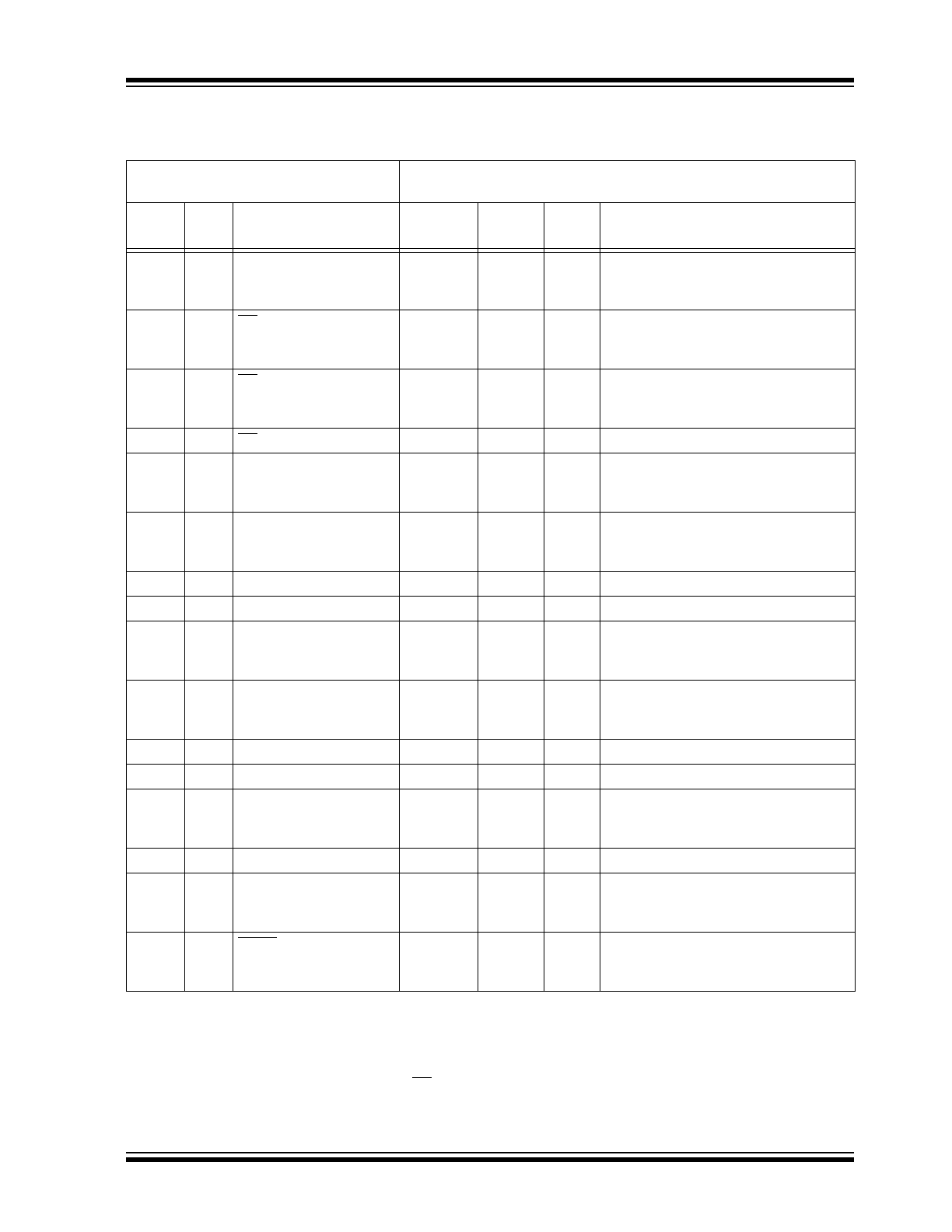
TABLE 1-2:
AC CHARACTERISTICS
AC CHARACTERISTICS
Industrial (I):
T
AMB
= -40°C to +85°C
V
CC
= 1.8V to 5.5V
Automotive (E): T
AMB
= -40°C to +125°C
V
CC
= 2.5V to 5.5V
Param.
No.
Sym.
Characteristic
Min.
Max.
Units
Test Conditions
1
F
CLK
Clock Frequency
—
—
—
10
5
3
MHz
MHz
MHz
4.5V
≤
V
CC
≤
5.5V
2.5V
≤
V
CC
<
4.5V
1.8V
≤
V
CC
<
2.5V
2
T
CSS
CS Setup Time
50
100
150
—
—
—
ns
ns
ns
4.5V
≤
V
CC
≤
5.5V
2.5V
≤
V
CC
<
4.5V
1.8V
≤
V
CC
<
2.5V
3
T
CSH
CS Hold Time
100
200
250
—
—
—
ns
ns
ns
4.5V
≤
V
CC
≤
5.5V
2.5V
≤
V
CC
<
4.5V
1.8V
≤
V
CC
<
2.5V
4
T
CSD
CS Disable Time
50
—
ns
—
5
Tsu
Data Setup Time
10
20
30
—
—
—
ns
ns
ns
4.5V
≤
V
CC
≤
5.5V
2.5V
≤
V
CC
<
4.5V
1.8V
≤
V
CC
<
2.5V
6
T
HD
Data Hold Time
20
40
50
—
—
—
ns
ns
ns
4.5V
≤
V
CC
≤
5.5V
2.5V
≤
V
CC
<
4.5V
1.8V
≤
V
CC
<
2.5V
7
T
R
CLK Rise Time
—
500
ns
(Note 1)
8
T
F
CLK Fall Time
—
500
ns
(Note 1)
9
T
HI
Clock High Time
50
100
150
—
—
—
ns
ns
ns
4.5V
≤
V
CC
≤
5.5V
2.5V
≤
V
CC
<
4.5V
1.8V
≤
V
CC
<
2.5V
10
T
LO
Clock Low Time
50
100
150
—
—
—
ns
ns
ns
4.5V
≤
V
CC
≤
5.5V
2.5V
≤
V
CC
<
4.5V
1.8V
≤
V
CC
<
2.5V
11
T
CLD
Clock Delay Time
50
—
ns
—
12
T
CLE
Clock Enable Time
50
—
ns
—
13
T
V
Output Valid from Clock
Low
—
—
—
50
100
160
ns
ns
ns
4.5V
≤
V
CC
≤
5.5V
2.5V
≤
V
CC
<
4.5V
1.8V
≤
V
CC
<
2.5V
14
T
HO
Output Hold Time
0
—
ns
(Note 1)
15
T
DIS
Output Disable Time
—
—
—
40
80
160
ns
ns
ns
4.5V
≤
V
CC
≤
5.5V (Note 1)
2.5V
≤
V
CC
<
4.5V (Note 1)
1.8V
≤
V
CC
<
2.5V (Note 1)
16
T
HS
HOLD Setup Time
20
40
80
—
—
—
ns
ns
ns
4.5V
≤
V
CC
≤
5.5V
2.5V
≤
V
CC
<
4.5V
1.8V
≤
V
CC
<
2.5V
Note 1: This parameter is periodically sampled and not 100% tested.
2: This parameter is not tested but ensured by characterization. For endurance estimates in a specific
application, please consult the Total Endurance™ Model which can be obtained from our web site:
www.microchip.com.
3: T
WC
begins on the rising edge of CS after a valid write sequence and ends when the internal write cycle
is complete.
25XX080A/B
DS21808D-page 4
©
2007 Microchip Technology Inc.
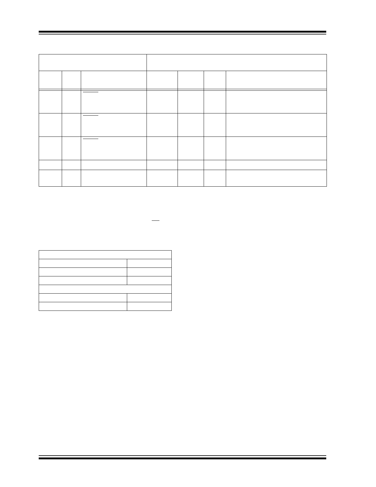
TABLE 1-3:
AC TEST CONDITIONS
17
T
HH
HOLD Hold Time
20
40
80
—
—
—
ns
ns
ns
4.5V
≤
V
CC
≤
5.5V
2.5V
≤
V
CC
<
4.5V
1.8V
≤
V
CC
<
2.5V
18
T
HZ
HOLD Low to Output
High-Z
30
60
160
—
—
—
ns
ns
ns
4.5V
≤
V
CC
≤
5.5V (Note 1)
2.5V
≤
V
CC
<
4.5V (Note 1)
1.8V
≤
V
CC
<
2.5V (Note 1)
19
T
HV
HOLD High to Output
Valid
30
60
160
—
—
—
ns
ns
ns
4.5V
≤
V
CC
≤
5.5V
2.5V
≤
V
CC
<
4.5V
1.8V
≤
V
CC
<
2.5V
20
T
WC
Internal Write Cycle Time
—
5
ms
(Note 3)
21
—
Endurance
1,000,000
—
E/W
Cycles
(Note 2)
TABLE 1-2:
AC CHARACTERISTICS (CONTINUED)
AC CHARACTERISTICS
Industrial (I):
T
AMB
= -40°C to +85°C
V
CC
= 1.8V to 5.5V
Automotive (E): T
AMB
= -40°C to +125°C
V
CC
= 2.5V to 5.5V
Param.
No.
Sym.
Characteristic
Min.
Max.
Units
Test Conditions
Note 1: This parameter is periodically sampled and not 100% tested.
2: This parameter is not tested but ensured by characterization. For endurance estimates in a specific
application, please consult the Total Endurance™ Model which can be obtained from our web site:
www.microchip.com.
3: T
WC
begins on the rising edge of CS after a valid write sequence and ends when the internal write cycle
is complete.
AC Waveform:
V
LO
= 0.2V
—
V
H I
= V
CC
- 0.2V
(Note 1)
V
H I
= 4.0V
(Note 2)
Timing Measurement Reference Level
Input
0.5 V
CC
Output
0.5 V
CC
Note 1: For V
CC
≤
4.0V
2: For V
CC
> 4.0V
©
2007 Microchip Technology Inc.
DS21808D-page 5
25XX080A/B
FIGURE 1-1:
HOLD TIMING
FIGURE 1-2:
SERIAL INPUT TIMING
FIGURE 1-3:
SERIAL OUTPUT TIMING
CS
SCK
SO
SI
HOLD
17
16
16
17
19
18
don’t care
5
high-impedance
n+2
n+1
n
n-1
n
n+2
n+1
n
n
n-1
CS
SCK
SI
SO
6
5
8
7
11
3
LSB in
MSB in
high-impedance
12
Mode 1,1
Mode 0,0
2
4
CS
SCK
SO
10
9
13
MSB out
ISB out
3
15
don’t care
SI
Mode 1,1
Mode 0,0
14

25XX080A/B
DS21808D-page 6
©
2007 Microchip Technology Inc.
2.0
FUNCTIONAL DESCRIPTION
2.1
Principles of Operation
The 25XX080A/B are 1024 byte Serial EEPROMs
designed to interface directly with the Serial
Peripheral Interface (SPI) Port of many of today’s
popular microcontroller families, including
Microchip’s PIC
®
microcontrollers. It may also inter-
face with microcontrollers that do not have a built-in
Synchronous Serial Port by using discrete
I/O lines programmed properly with the software.
The 25XX080A/B contains an 8-bit instruction register.
The device is accessed via the SI pin, with data being
clocked in on the rising edge of SCK. The CS pin must
be low and the HOLD pin must be high for the entire
operation.
Table 2-1 contains a list of the possible instruction
bytes and format for device operation. All instructions,
addresses, and data are transferred MSB first, LSB
last.
Data (SI) is sampled on the first rising edge of SCK
after CS goes low. If the clock line is shared with other
peripheral devices on the SPI bus, the user can assert
the HOLD input and place the 25XX080A/B in ‘HOLD’
mode. After releasing the HOLD pin, operation will
resume from the point when the HOLD was asserted.
2.2
Read Sequence
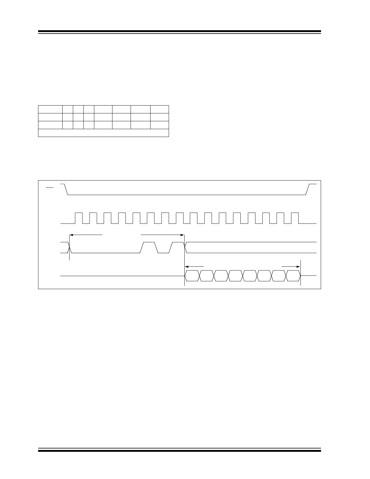
The device is selected by pulling CS low. The 8-bit read
instruction is transmitted to the 25XX080A/B followed
by the 16-bit address, with the six MSBs of the address
being don’t care bits. After the correct read instruction
and address are sent, the data stored in the memory at
the selected address is shifted out on the SO pin. The
data stored in the memory at the next address can be
read sequentially by continuing to provide clock pulses.
The internal address pointer is automatically
incremented to the next higher address after each byte
of data is shifted out. When the highest address is
reached (03FFh), the address counter rolls over to
address 0000h allowing the read cycle to be continued
indefinitely. The read operation is terminated by raising
the CS pin (Figure 2-1).
2.3
Write Sequence
Prior to any attempt to write data to the 25XX080A/B,
the write enable latch must be set by issuing the
WREN
instruction (Figure 2-4). This is done by setting CS low
and then clocking out the proper instruction into the
25XX080A/B. After all eight bits of the instruction are
transmitted, the CS must be brought high to set the
write enable latch. If the write operation is initiated
immediately after the
WREN
instruction without CS
being brought high, the data will not be written to the
array because the write enable latch will not have been
properly set.
Once the write enable latch is set, the user may
proceed by setting the CS low, issuing a
WRITE
instruction, followed by the 16-bit address, with the six
MSBs of the address being don’t care bits, and then the
data to be written. Up to 16 bytes (25XX080A) or 32
bytes (25XX080B) of data can be sent to the device
before a write cycle is necessary. The only restriction is
that all of the bytes must reside in the same page.
For the data to be actually written to the array, the CS
must be brought high after the Least Significant bit (D0)
of the n
th
data byte has been clocked in. If CS is
brought high at any other time, the write operation will
not be completed. Refer to Figure 2-2 and Figure 2-3
for more detailed illustrations on the byte write
sequence and the page write sequence respectively.
While the write is in progress, the Status Register may
be read to check the status of the WPEN, WIP, WEL,
BP1 and BP0 bits (Figure 2-6). A read attempt of a
memory array location will not be possible during a
write cycle. When the write cycle is completed, the
write enable latch is reset.
Note:
Page write operations are limited to writing
bytes within a single physical page,
regardless of the number of bytes
actually being written. Physical page
boundaries start at addresses that are
integer multiples of the page buffer size (or
‘page size’) and, end at addresses that are
integer multiples of page size - 1. If a Page
Write command attempts to write across a
physical page boundary, the result is that
the data wraps around to the beginning of
the current page (overwriting data
previously stored there), instead of being
written to the next page as might be
expected. It is therefore necessary for the
application software to prevent page write
operations that would attempt to cross a
page boundary.
©
2007 Microchip Technology Inc.
DS21808D-page 7
25XX080A/B
Block Diagram
FIGURE 2-1:
READ SEQUENCE
SI
SO
SCK
CS
HOLD
WP
Status
Register
I/O Control
Memory
Control
Logic
X
Dec
HV Generator
EEPROM
Array
Page Latches
Y Decoder
Sense Amp.
R/W Control
Logic
V
CC
V
SS
TABLE 2-1:
INSTRUCTION SET
Instruction Name
Instruction Format
Description
READ
0000 0011
Read data from memory array beginning at selected address
WRITE
0000 0010
Write data to memory array beginning at selected address
WRDI
0000 0100
Reset the write enable latch (disable write operations)
WREN
0000 0110
Set the write enable latch (enable write operations)
RDSR
0000 0101
Read Status Register
WRSR
0000 0001
Write Status Register
SO
SI
SCK
CS
0
2
3
4
5
6
7
8
9 10 11
21 22 23 24 25 26 27 28 29 30 31
1
0
1
0
0
0
0
0
1
15 14 13 12
2
1
0
7
6
5
4
3
2
1
0
instruction
16-bit address
data out
high-impedance
25XX080A/B
DS21808D-page 8
©
2007 Microchip Technology Inc.
FIGURE 2-2:
BYTE WRITE SEQUENCE
FIGURE 2-3:
PAGE WRITE SEQUENCE
SO
SI
CS
9 10 11
21 22 23 24 25 26 27 28 29 30 31
0
0
0
0
0
0
0
1
15 14 13 12
2
1
0
7
6
5
4
3
2
1
0
instruction
16-bit address
data byte
high-impedance
SCK
0
2
3
4
5
6
7
1
8
Twc
SI
CS
9 10 11
21 22 23 24 25 26 27 28 29 30 31
0
0
0
0
0
0
0
1
15 14 13 12
2
1
0
7
6
5
4
3
2
1
0
instruction
16-bit address
data byte 1
SCK
0
2
3
4
5
6
7
1
8
SI
CS
41 42 43
46 47
7
6
5
4
3
2
1
0
data byte n (16/32 max)
SCK
32
34 35 36 37 38 39
33
40
7
6
5
4
3
2
1
0
data byte 3
7
6
5
4
3
2
1
0
data byte 2
44 45
©
2007 Microchip Technology Inc.
DS21808D-page 9
25XX080A/B
2.4
Write Enable (
WREN
) and Write
Disable (
WRDI
)
The 25XX080A/B contains a write enable latch. See
Table 2-4 for the Write-Protect Functionality Matrix.
This latch must be set before any write operation will be
completed internally. The
WREN
instruction will set the
latch, and the
WRDI
will reset the latch.
The following is a list of conditions under which the
write enable latch will be reset:
• Power-up
•
WRDI
instruction successfully executed
•
WRSR
instruction successfully executed
•
WRITE
instruction successfully executed
FIGURE 2-4:
WRITE ENABLE SEQUENCE (
WREN
)
FIGURE 2-5:
WRITE DISABLE SEQUENCE (
WRDI
)
SCK
0
2
3
4
5
6
7
1
SI
high-impedance
SO
CS
0
1
0
0
0
0
0
1
SCK
0
2
3
4
5
6
7
1
SI
high-impedance
SO
CS
0
1
0
0
0
0
0
10
25XX080A/B
DS21808D-page 10
©
2007 Microchip Technology Inc.
2.5
Read Status Register Instruction
(
RDSR
)
The Read Status Register instruction (
RDSR
) provides
access to the Status Register. The Status Register may
be read at any time, even during a write cycle. The
Status Register is formatted as follows:
TABLE 2-2:
STATUS REGISTER
The Write-In-Process (WIP) bit indicates whether the
25XX080A/B is busy with a write operation. When set
to a ‘
1
’, a write is in progress, when set to a ‘
0
’, no write
is in progress. This bit is read-only.
The Write Enable Latch (WEL) bit indicates the status
of the write enable latch and is read only. When set to
a ‘
1
’, the latch allows writes to the array or the Status
Register, when set to a ‘
0
’, the latch prohibits writes to
the array or the Status Register. The state of this bit can
always be updated via the
WREN
or
WRDI
commands
regardless of the state of write protection on the Status
Register. These commands are shown in Figure 2-4
and Figure 2-5.
The Block Protection (BP0 and BP1) bits indicate
which blocks are currently write-protected. These bits
are set by the user issuing the
WRSR
instruction, which
is in Figure 2-7. These bits are nonvolatile and are
shown in Table 2-3.
See Figure 2-6 for the
RDSR
timing sequence.
FIGURE 2-6:
READ STATUS REGISTER TIMING SEQUENCE (
RDSR
)
7
6
5
4
3
2
1
0
W/R
–
–
–
W/R
W/R
R
R
WPEN
X
X
X
BP1
BP0
WEL
WIP
W/R = writable/readable. R = read-only.
SO
SI
CS
9
10
11
12
13
14
15
1
1
0
0
0
0
0
0
7
6
5
4
2
1
0
instruction
data from Status Register
high-impedance
SCK
0
2
3
4
5
6
7
1
8
3