
2003-2013 Microchip Technology Inc.
DS21762B-page 1
MCP1601
Features
• Input Range of 2.7V to 5.5V
• 3 Operating Modes: PWM, PFM and LDO
• Integrated BUCK and Synchronous Switches
• Ceramic or Electrolytic Input/Output Filtering
Capacitors
• 750 kHz Fixed Switching Frequency
• Oscillator Synchronization to 1 MHz PWM Mode
• Auto-Switching from PWM/PFM Operation
• 100% Duty Cycle Capable for Low Input Voltage
• 500 mA Continuous Output Current Capability
• Integrated Under-Voltage Lock-Out Protection
• Integrated Over-Temperature Protection
• Integrated Soft Start Circuitry
• Low Output Voltage Capability to 0.9V
• Temperature Range: -40°C to +85ºC
• Small 8-Pin MSOP Package
Applications
• Low Power Handheld CPUs and DSPs
• Cellular Phones
• Organizers and PDAs
• Digital Cameras
• +5V or +3.3V Distributed Voltages
• USB Powered Devices
Package Type
Description
The MCP1601 is a fully integrated synchronous BUCK
(step down) DC/DC converter for battery powered sys-
tems. With an input operating range of 2.7V to 5.5V, the
MCP1601 is ideal for applications being powered by
one single cell Li-Ion, 2 to 3 cell NiMH, NiCd or alkaline
sources. Output voltages can range from 0.9V to V
IN
to
accommodate a wide range of applications. Efficiency
can exceed 92% while operating at 750 kHz with load
current capability up to 500 mA. The MCP1601 is used
to minimize space, cost and wasted energy.
The PWM mode switching frequency is internally set to
a fixed 750 kHz allowing the use of low profile, surface
mount inductors and ceramic capacitors while
maintaining a typical efficiency of 92%.
The MCP1601 is capable of three distinct operating
modes: PWM, PFM and Low Drop Out.
When operating in PWM (pulse width modulation)
mode, the DC/DC converter switches at a single high
frequency determined by either the internal 750 kHz
oscillator or external synchronization frequency.
For applications that operate at very light to no load for
extended periods of time, the MCP1601 is capable of
operating in PFM (pulse frequency modulation mode)
to reduce the number of switching cycles/sec and
consume less energy.
The third mode of operation (LDO mode) occurs when
the input voltage approaches the output voltage and the
BUCK duty cycle approaches 100%. The MCP1601 will
enter a low drop out mode and the high-side P-Channel
BUCK switch will saturate, providing the output with the
maximum voltage possible.
The MCP1601 has integrated over-current protection,
over-temperature protection and UVLO (Under Voltage
Lockout) to provide for a fail safe solution with no
external components.
The MCP1601 is available in the 8-pin MSOP package,
with an operating temperature range of -40°C to +85°C.
8-Pin MSOP
V
IN
SHDN
FB
A
GND
L
X
P
GND
V
OUT
SYNC/PWM
1
2
3
4
8
7
6
5
MCP1601
500 mA Synchronous BUCK Regulator
MCP1601
DS21762B-page 2
2003-2013 Microchip Technology Inc.
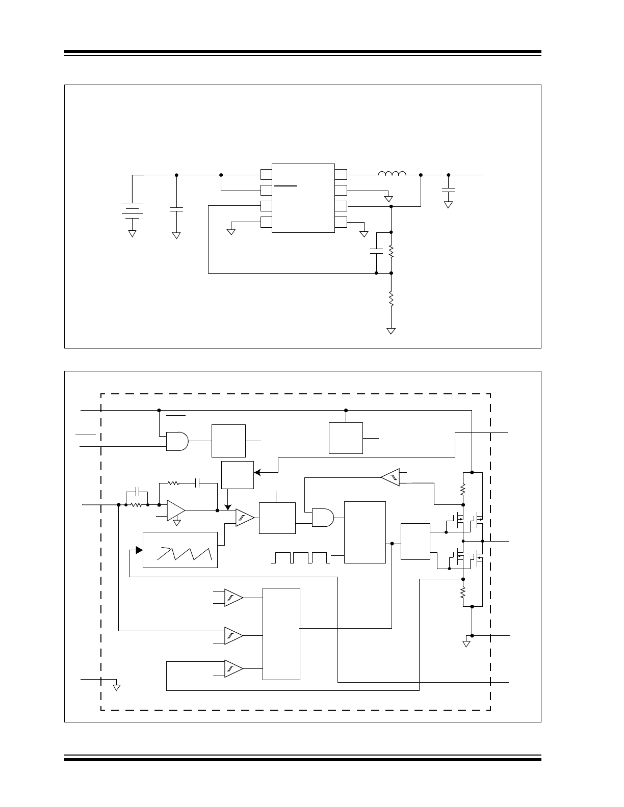
Typical Application
Functional Block Diagram
V
OUT
P
GND
L
X
SHDN
V
IN
1
2
3
4
8
7
6
5
MCP1601
FB
SYNC/
A
GND
Input
Voltage
2.7V-4.2V
C
IN
10 µF
10 µH
C
OUT
10 µF
R
1
250 k
(for 1.8V)
R
2
200 k
Typical Application (2.7V to 4.2V)
I
OUT
= 0 mA to 400 mA
C
OUT
Range
10 µF to 47 µF
L Range
10 µH to 22 µH
C
1
47 pF
V
OUT
Range
1.2V to 3.3V
PWM
+
-
EA
C
COMP
FB
R
COMP
Feedforward Oscillator
K*V
IN
Duty
Clamp
10% - 90%
PWM Latch
R
OUT
Inset
Timing
0.8V
I
SENSE
P
V
REF
S
SQW
V
IN
SHDN
Internal
Circuit
UVLO
Enable Out
A
GND
A
GND
A
GND
PFM Comparator
Internal
Band Gap
Reference
Buffered 0.8V Output
V
REF
SYNC/PWM
V
REF
I
SENSE
P
I
SENSE
N
PFM Mode
Timing
L
X
V
OUT
P
GND
P
GND
Soft Start
I
SENSE
N
Duty
Clamp
800 k
12 pF
10 pF
3 M
-
-
+
V
REF
-
-
+
-
+
Enable
Cycle
Cycle
2003-2013 Microchip Technology Inc.
DS21762B-page 3
MCP1601
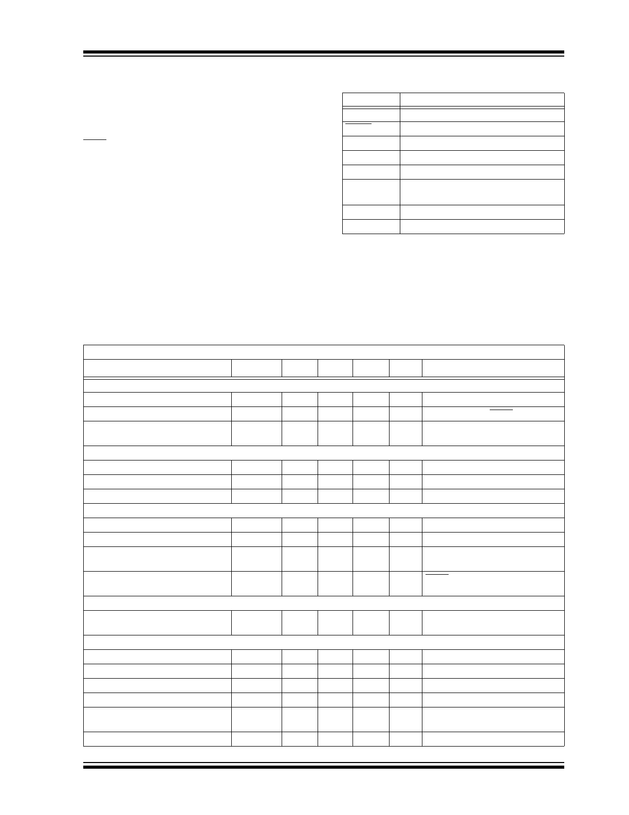
1.0
ELECTRICAL
CHARACTERISTICS
Absolute Maximum Ratings †
V
IN
- A
GND
......................................................................6.0V
SHDN, FB, SYNC/PWM, V
OUT
..... (A
GND
-0.3V) to (V
IN
+0.3V)
L
X
to P
GND
................................................ -0.3V to (V
IN
+0.3V)
P
GND
to A
GND
.................................................. -0.3V to +0.3V
Output Short Circuit Current .................................continuous
Storage temperature .....................................-65°C to +150°C
Ambient Temp. with Power Applied ................-40°C to +85°C
Operating Junction Temperature...................-40°C to +125°C
ESD protection on all pins
4 kV
† Notice: Stresses above those listed under “Maximum rat-
ings” may cause permanent damage to the device. This is a
stress rating only and functional operation of the device at
those or any other conditions above those indicated in the
operational listings of this specification is not implied. Expo-
sure to maximum rating conditions for extended periods may
affect device reliability.
PIN FUNCTION TABLE
NAME
FUNCTION
V
IN
Input Source Voltage
SHDN
Device Shutdown Pin
FB
Output Voltage Feedback Input
A
GND
Analog Ground
V
OUT
Sensed Output Voltage
SYNC/PWM
Synchronous Clock input or PWM/
PFM select
P
GND
Power Ground
L
X
Output Inductor Node
ELECTRICAL SPECIFICATIONS
Electrical Specifications: Unless otherwise indicated, V
IN
=4.2V, V
OUT
=1.8V, I
LOAD
= 10 mA, T
A
=-40°C to +85°C.
Parameters
Sym
Min
Typ
Max
Units
Conditions
Power Input Requirements
Voltage
V
IN
2.7
—
5.5
V
I
LOAD
= 0 mA to 500 mA
Shutdown Current
I(V
IN
)
—
0.05
1.0
µA
Shutdown Mode (SHDN = GND)
PFM Mode Current
I(V
IN
)
—
119
180
µA
SYNC/PWM = GND, PFM Mode
(I
LOAD
= 0 mA)
Oscillator Section
Internal Oscillator Frequency
F
OSC
650
750
850
kHz
SYNC/PWM = V
IN
External Oscillator Capture Range
F
SYNC
850
—
1000
kHz
F
SYNC
> F
OSC
External Oscillator Duty Cycle
F
SYN-FALL
10
—
90
%
F
SYNC
= 1 MHz
Internal Power Switches
R
DSon
P-CHANNEL
R
DSon-P
—
500
—
m
I
P
=100 mA, T
A
=+25°C, V
IN
=4.2V
R
DSon
N-CHANNEL
R
DSon-N
—
500
—
m
I
N
=100 mA, T
A
=+25°C, V
IN
=4.2V
Dropout Voltage
V
DROPOUT
—
250
—
mV
V
OUT
= 2.7V, I
LOAD
= 300 mA,
T
A
=+25°C, V
DROPOUT
=97%V
OUT
Pin Leakage Current
I
LX
-1.0
—
1.0
µA
SHDN = 0V, V
IN
= 5.5V, L
X
= 0V, L
X
=
5.5V
Output PWM Mode
Peak Current Limit
I
PEAK-PWM
—
1.0
—
A
PWM Mode, SYNC/PWM = V
IN,
T
A
=
+25°C
Output Voltage
Output Voltage Range
V
OUT
0.9
—
V
IN
V
Reference Feedback Voltage
V
FB
0.78
0.8
0.82
V
Feedback Input Bias Current
I
VFB
—
0.1
—
nA
Line Regulation
V
LINE-REG
—
0.1
—
%/V
V
IN
=2.7V to 5.5V, I
LOAD
=10 mA
Load Regulation
V
LOAD-REG
—
1.5
—
%
V
IN
= 3.6V,
I
LOAD
= 0 mA to 300 mA
Start-Up Time
T
START
—
0.5
—
ms
PWM Mode, SYNC/PWM=V
IN

MCP1601
DS21762B-page 4
2003-2013 Microchip Technology Inc.
TEMPERATURE SPECIFICATIONS
Protection Features
Average Short Circuit Current
—
890
—
mA
R
LOAD
< 1 ohm
Under-Voltage Lockout
UVLO
2.4
—
2.7
V
For V
IN
decreasing
Under-Voltage Lockout Hysteresis
UVLO-
HYS
—
190
—
mV
Thermal Shutdown
T
SHD
—
160
—
°C
Thermal Shutdown Hysteresis
T
SHD-HYS
—
10
—
°C
Interface Signals (SHDN, SYNC/PWM)
Logic Low Input
V
IN-HIGH
—
—
15
% of
V
IN
Logic High Input
V
IN-HIGH
45
—
—
% of
V
IN
Input Leakage Current
I
IN-LK
—
—
0.1
µA
Electrical Specifications: Unless otherwise noted, all parameters apply at V
DD
= 2.7V to 5.5V
Parameters
Symbol
Min
Typ
Max
Units
Conditions
Temperature Ranges
Specified Temperature Range
T
A
-40
—
+85
°C
Operating Junction Temperature Range
T
J
-40
—
+125
°C
Storage Temperature Range
T
A
-65
—
+150
°C
Thermal Package Resistances
Thermal Resistance, 8 Pin MSOP
JA
—
208
—
°C/W
Single-Layer SEMI G42-88
Board, Natural Convection
ELECTRICAL SPECIFICATIONS
(CONTINUED)
Electrical Specifications: Unless otherwise indicated, V
IN
=4.2V, V
OUT
=1.8V, I
LOAD
= 10 mA, T
A
=-40°C to +85°C.
Parameters
Sym
Min
Typ
Max
Units
Conditions
2003-2013 Microchip Technology Inc.
DS21762B-page 5
MCP1601
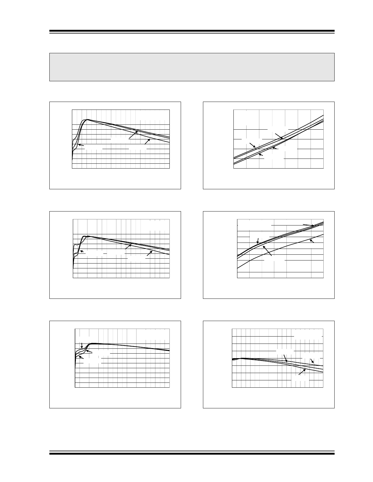
2.0
TYPICAL PERFORMANCE CURVES
Note: Unless otherwise indicated, V
IN
= 4.2V, V
OUT
= 1.8V, L = 10 µH, C
OUT
= 10 µF (X5R Ceramic), C
IN
= 10 µF (X5R
Ceramic), SYNC/PWM=V
IN
.
FIGURE 2-1:
Efficiency vs. Load Current
(V
OUT
= 1.2V).
FIGURE 2-2:
Efficiency vs. Load Current
(V
OUT
= 1.8V).
FIGURE 2-3:
Efficiency vs. Load Current
(V
OUT
= 3.3V).
FIGURE 2-4:
PFM Mode Quiescent
Current vs. Input Voltage.
FIGURE 2-5:
Oscillator Frequency vs.
Input Voltage.
FIGURE 2-6:
Output Voltage vs. Load
Current.
Note:
The graphs and tables provided following this note are a statistical summary based on a limited number of
samples and are provided for informational purposes only. The performance characteristics listed herein
are not tested or guaranteed. In some graphs or tables, the data presented may be outside the specified
operating range (e.g., outside specified power supply range) and therefore outside the warranted range.
40
50
60
70
80
90
100
0
100
200
300
400
500
Load Current (mA)
E
fficiency (%
)
V
OUT
= 1.2V
Auto PWM/PFM
V
IN
= 2.7V
V
IN
= 3.6V
V
IN
= 4.2V
50
60
70
80
90
100
110
0
100
200
300
400
500
Load Current (mA)
E
fficiency (%
)
V
OUT
= 1.8V
Auto PWM/PFM
V
IN
= 2.7V
V
IN
= 3.6V
V
IN
= 4.2V
50
60
70
80
90
100
110
0
100
200
300
400
500
Load Current (mA)
E
fficiency (%
)
V
OUT
= 3.3V
Auto PWM/PFM
V
IN
= 5.0V
V
IN
= 4.5V
V
IN
= 5.5V
100
110
120
130
2.7
3.1
3.5
3.9
4.3
4.7
5.1
5.5
Input Voltage (V)
P
F
M Mode Quiescent C
u
rr
e
nt
(µA
)
V
OUT
= 1.8V
PFM Mode
I
LOAD
= 0
T
A
= - 40°C
T
A
= + 0°C
T
A
= + 85°C
T
A
= + 25°C
680.0
700.0
720.0
740.0
760.0
780.0
2.7
3.1
3.5
3.9
4.3
4.7
5.1
5.5
Input Voltage (V)
In
ter
n
al Oscillato
r F
req
u
e
n
cy
(kH
z
)
T
A
= + 125°C
T
A
= - 40°C
T
A
= + 25°C
T
A
= 0°C
I
LOAD
= 10 mA
Forced PWM Mode
1.100
1.125
1.150
1.175
1.200
1.225
1.250
1.275
1.300
0
100
200
300
400
500
Load Current (mA)
Output V
o
ltage (V
)
V
OUT
= 1.2V
Auto PWM/PFM
V
IN
= 2.7V
V
IN
= 3.6V
V
IN
= 4.2V
MCP1601
DS21762B-page 6
2003-2013 Microchip Technology Inc.
Note: Unless otherwise indicated, V
IN
= 4.2V, V
OUT
= 1.8V, L = 10 µH, C
OUT
= 10 µF (X5R Ceramic), C
IN
= 10 µF (X5R
Ceramic), SYNC/PWM=V
IN
.
FIGURE 2-7:
Output Voltage vs. Load
Current.
FIGURE 2-8:
Output Voltage vs. Load
Current.
FIGURE 2-9:
Input to Output Voltage
Differential for 100% Duty Cycle vs. Load
Current.
FIGURE 2-10:
Switch Leakage vs.
Temperature.
FIGURE 2-11:
Typical PWM Mode of
Operation Waveforms.
FIGURE 2-12:
Typical PFM Mode of
Operation Waveforms.
1.700
1.720
1.740
1.760
1.780
1.800
1.820
0
100
200
300
400
500
Load Current (mA)
Output V
o
tlage (V
)
V
OUT
= 1.8V
Auto PWM/PFM
V
IN
= 2.7V
V
IN
= 3.6V
V
IN
= 4.2V
3.10
3.13
3.15
3.18
3.20
3.23
3.25
3.28
3.30
3.33
3.35
0
100
200
300
400
500
Load Current (mA)
Output V
o
ltage (V
)
V
OUT
= 3.3V
Auto PWM/PFM
V
IN
= 4.5V
V
IN
= 5.0V
V
IN
= 5.5V
0
50
100
150
200
250
300
350
400
450
0
100
200
300
400
500
Load Current (mA)
D
ropout V
o
lt
age (m
V
)
V
OUT
= 3.3V
V
OUT
= 2.7V
Dropout = (V
IN
-V
OUT
) in mV @ 97% of V
OUT
0.0
1.5
3.0
4.5
-40
-15
10
35
60
85
Ambient Temperature (°C)
L
X
Leakage C
u
rr
e
nt (nA
)
V
IN
= 5.0V
Synchronous N
Channel
BUCK Switch P
Channel
2003-2013 Microchip Technology Inc.
DS21762B-page 7
MCP1601
Note: Unless otherwise indicated, V
IN
= 4.2V, V
OUT
= 1.8V, L = 10 µH, C
OUT
= 10 µF (X5R Ceramic), C
IN
= 10 µF (X5R
Ceramic), SYNC/PWM=V
IN
.
FIGURE 2-13:
Typical Startup From
Shutdown Waveform.
FIGURE 2-14:
Startup From 0V Input.
FIGURE 2-15:
Load Step Response
(Forced PWM).
FIGURE 2-16:
Load Step Response (PFM
to PWM).
FIGURE 2-17:
Line Step Response
(Forced PWM).
FIGURE 2-18:
Line Step Response (PFM
Mode).
MCP1601
DS21762B-page 8
2003-2013 Microchip Technology Inc.
Note: Unless otherwise indicated, V
IN
= 4.2V, V
OUT
= 1.8V, L = 10 µH, C
OUT
= 10 µF (X5R Ceramic), C
IN
= 10 µF (X5R
Ceramic), SYNC/PWM=V
IN
.
FIGURE 2-19:
Typical Output Ripple
Voltage (Forced PWM Mode).
FIGURE 2-20:
Typical Output Ripple
Voltage (PFM Mode).
FIGURE 2-21:
External Oscillator
Synchronization.
2003-2013 Microchip Technology Inc.
DS21762B-page 9
MCP1601
3.0
PIN FUNCTIONS
TABLE 3-1:
PIN FUNCTION TABLE
3.1
Input Voltage (V
IN
)
Connect the unregulated input voltage source to V
IN
. If
the input voltage source is located more than several
inches away, or is a battery, a typical input capacitor of
10 µF is recommended.
3.2
Shutdown Input (SHDN)
Connect SHDN to a logic low input to force the device
into a shutdown low quiescent current mode. When in
shutdown, both the P-Channel and N-Channel
switches are turned off, in addition to the internal oscil-
lator and other circuitry. When connected to a logic high
input, the device will operate in the selected mode.
3.3
Feedback Input (FB)
Connect FB to an external resistor divider
to set output
voltage regulation. The feedback pin is typically equal
to 0.8V. See Section 5.0, “Applications Information”, for
details in selecting feedback resistors.
3.4
Analog Ground Return (A
GND
)
Tie all small signal ground returns to A
GND
. (See
Section 5.6, “Printed Circuit Board Layout”, for details).
3.5
Oscillator Synchronization or
PWM/ PFM Select Mode Input
(SYNC/PWM)
Connect an external oscillator to SYNC/PWM to syn-
chronize. With an external oscillator present, the device
is forced into a PWM-only mode of operation. For inter-
nal oscillator operation, the SYNC/PWM pin is tied high
to operate in a forced PWM-only mode and low for a
PWM/PFM mode of operation.
3.6
Output Voltage Sense (V
OUT
)
Connect the output voltage directly to V
OUT
for sensing.
3.7
Power Ground Return (P
GND
)
Connect all large signal ground returns to P
GND
. (See
Section 5.6, “Printed Circuit Board Layout”, for details).
3.8
BUCK Inductor Connection (L
X
)
Connect L
X
directly to the BUCK inductor. This pin car-
ries large signal-level currents and all connections
should be as short and wide as possible. (See
Section 5.6, “Printed Circuit Board Layout”, for details).
Pin
Name
Function
1
V
IN
Input Voltage
2
SHDN
Shutdown Input
3
FB
Feedback Input
4
A
GND
Analog Ground Return
5
SYNC/
PWM
Oscillator Synchronization or
PWM/ PFM Select Mode Input
6
V
OUT
Sensed Output Voltage Input
7
P
GND
Power Ground Return
8
L
X
BUCK Inductor Output

MCP1601
DS21762B-page 10
2003-2013 Microchip Technology Inc.
4.0
DEVICE OPERATION
The MCP1601 is a synchronous DC/DC converter with
integrated switches. Developed to provide high effi-
ciency across a wide line and load range, the
MCP1601 integrates the three modes of operation
described below. In addition to three operating modes,
the MCP1601 also integrates many features that mini-
mize external circuitry, saving board space and cost.
With two external resistors used to set the output volt-
age, the MCP1601 output is adjustable from 0.9V to
V
IN
.
4.1
Operating Modes
The MCP1601 has three distinct modes of operation,
with each one optimized for a specific operating condi-
tion commonly encountered in handheld portable
power applications.
4.1.1
FEEDFORWARD VOLTAGE PULSE
WIDTH MODULATION (PWM) MODE
The Pulse Width Modulation (PWM) mode of operation
is desired when operating from typical to maximum out-
put currents with the proper head room voltage at the
input. This mode of operation optimizes efficiency and
noise by switching at a fixed frequency. Typical output
ripple voltage is less than 10 mV when using a 10 µH
inductor and 10 µF ceramic capacitor. The internal
operating frequency of the MCP1601 is 750 kHz, nom-
inal. The duty cycle, or “ON” time, of the high-side, inte-
grated, P-Channel MOSFET is determined by the
continuous mode BUCK transfer function. For the con-
tinuous inductor current case, the duty cycle can be
approximated by V
OUT
/V
IN
. The integrated high-side
BUCK P-Channel switch will conduct for the “on” time.
At the end of the “on” time, the high-side P-Channel
switch is turned off and the integrated, low-side, N-
Channel synchronous switch is turned on to freewheel
the inductor current. The PWM mode architecture
employed in the MCP1601 is a feedforward voltage
mode control and feeds the input voltage into the PWM
oscillator ramp. This information is used to quickly
change the operating duty cycle in the event of a sud-
den input voltage change. The effects on the output
voltage are minimized. To force the MCP1601 into
PWM mode, the SYNC/PWM pin should be tied to a
logic high. The forced PWM mode should be used for
applications that require the fastest transient response
from light load to heavy load or applications that require
a single switching frequency independent of load.
An external oscillator between 850 kHz and 1 MHz can
be connected to the SYNC/PWM pin for synchroniza-
tion to an external clock source. The MCP1601 will
always operate in the PWM mode when synchronized
to an external oscillator.
4.1.2
PULSE FREQUENCY MODULATION
(PFM) MODE
The MCP1601 is also capable of operating in a pulse
frequency modulation mode. This mode of operation is
desired for applications that have very long periods of
inactivity and the output current requirement placed on
the MCP1601 is very low. By entering the PFM mode of
operation, the switching frequency becomes mainly a
function of load current and will decrease as the load
current decreases. By switching slower, the energy
used turning “on” and “off” the high-side P-Channel and
low-side N-Channel is reduced, making the PFM mode
more efficient with light output load currents. When
load activity is encountered, the MCP1601 will auto-
matically switch from the PFM mode to the fixed fre-
quency PWM mode by sensing the increase in load
current. The auto PWM/PFM mode is selected by plac-
ing a logic low at the SYNC/PWM input pin. If an exter-
nal clock is used to synchronize the MCP1601
switching frequency, the PFM mode is automatically
disabled.
To enter the PFM mode of operation, the SYNC/PWM
pin must be held to a logic low level and the peak induc-
tor current, sensed internal to the MCP1601, is below
the internal PFM threshold for more than 1024 clock
cycles. If both of these conditions are met, the
MCP1601 will enter the PFM mode. While in the PFM
mode, the MCP1601 will disable the low-side N-Chan-
nel switch to optimize efficiency at low operating cur-
rents. A cycle will begin by turning on the high-side
P-Channel switch and will end when the output voltage
exceeds a predetermined voltage set point. If the peak
inductor current exceeds the internal PFM mode cur-
rent threshold prior to the output voltage exceeding the
voltage set point, the load current has increased and
the MCP1601 will automatically switch to PWM opera-
tion. The typical hysteresis on the PFM comparator is
6 mV. The typical output ripple voltage is below 40 mV
when using a 10 µH inductor and 10 µF ceramic output
capacitor when V
IN
= 4.2V. For proper PFM mode oper-
ation, the value of the external inductor and the exter-
nal capacitor should be the same. For example, when
using a 10 µH inductor, a 10 µF capacitor should be
used. When using a 22 µH inductor, a 22 µF capacitor
should be used.
4.1.3
LOW DROP OUT (LDO) MODE
When the input voltage to the MCP1601 is decreasing
and approaches the set output voltage level, the duty
cycle increases to a maximum of 90% (typically). To
continue to regulate the output to as high a voltage as
possible, the MCP1601 enters the low drop out mode
of operation. In this mode, the high-side P-Channel
MOSFET acts like a saturated LDO. This mode allows
the operation of the load circuitry down to the minimum
input supply that is typical in battery-powered
applications.