
2002-2013 Microchip Technology Inc.
DS21755C-page 1
TC646B/TC648B/TC649B
Features
• Temperature-Proportional Fan Speed for Acoustic
Noise Reduction and Longer Fan Life
• Efficient PWM Fan Drive
• 3.0V to 5.5V Supply Range:
- Fan Voltage Independent of TC646B/
TC648B/TC649B Supply Voltage
- Supports any Fan Voltage
• FanSense
™
Fault Detection Circuit Protects
Against Fan Failure and Aids System Testing
(TC646B/TC649B)
• Automatic Shutdown Mode for “Green” Systems
• Supports Low Cost NTC/PTC Thermistors
• Over-Temperature Indication (TC646B/TC648B)
• Fan Auto-Restart
• Space-Saving 8-Pin MSOP Package
Applications
• Personal Computers & Servers
• LCD Projectors
• Datacom & Telecom Equipment
• Fan Trays
• File Servers
• General-Purpose Fan Speed Control
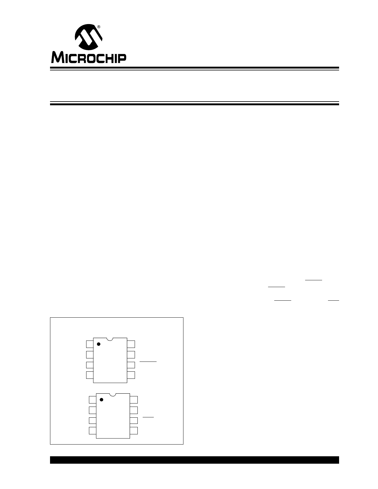
Package Types
Description
The TC646B/TC648B/TC649B devices are new ver-
sions of the existing TC646/TC648/TC649 fan speed
controllers. These devices are switch-mode fan speed
controllers that incorporate a new fan auto-restart func-
tion. Temperature-proportional speed control is accom-
plished using pulse width modulation. A thermistor (or
other voltage output temperature sensor) connected to
the V
IN
input supplies the required control voltage of
1.20V to 2.60V (typical) for 0% to 100% PWM duty
cycle. The auto-shutdown threshold/temperature is set
by a simple resistor divider on the V
AS
input. An inte-
grated Start-Up Timer ensures reliable fan motor start-
up at turn-on, coming out of shutdown mode, auto-
shutdown mode or following a transient fault. A logic
low applied to V
IN
(pin 1) causes fan shutdown.
The TC646B and TC649B also feature Microchip
Technology's proprietary FanSense technology for
increasing system reliability. In normal fan operation, a
pulse train is present at SENSE (pin 5). A missing-
pulse detector monitors this pin during fan operation. A
stalled, open or unconnected fan causes the TC646B/
TC649B device to turn the V
OUT
output on full (100%
duty cycle). If the fan fault persists (a fan current pulse
is not detected within a 32/f period), the FAULT output
goes low. Even with the FAULT output low, the V
OUT
output is on full during the fan fault condition in order to
attempt to restart the fan. FAULT (TC646B) or OTF
(TC648B) is also asserted if the PWM reaches 100%
duty cycle, indicating that maximum cooling capability
has been reached and a possible overheating condition
exists.
The TC646B, TC648B and TC649B devices are avail-
able in 8-pin plastic MSOP, SOIC and PDIP packages.
The specified temperature range of these devices is
-40 to +85ºC.
MSOP, PDIP, SOIC
1
2
3
4
V
DD
5
6
7
8
V
OUT
SENSE
V
IN
C
F
V
AS
GND
FAULT
TC646B
TC649B
1
2
3
4
V
DD
5
6
7
8
V
OUT
NC
V
IN
C
F
V
AS
GND
OTF
TC648B
PWM Fan Speed Controllers With Auto-Shutdown, Fan
Restart and FanSense™ Technology for Fault Detection
TC646B/TC648B/TC649B
DS21755C-page 2
2002-2013 Microchip Technology Inc.
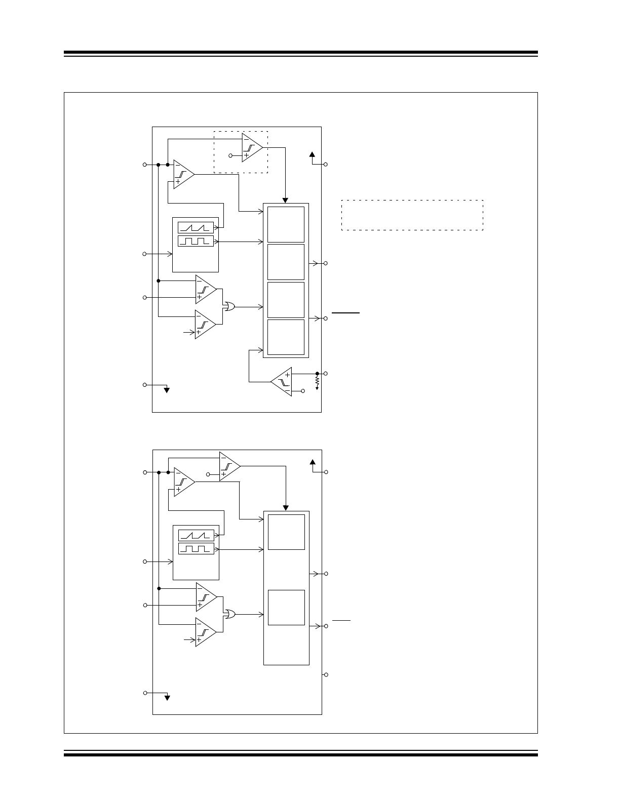
Functional Block Diagram
TC646B/TC649B
Note: The V
OTF
comparator
is for the TC646B device only.
70 mV
(typ)
V
OTF
10 k
V
SHDN
V
IN
C
F
V
AS
GND
V
DD
V
OUT
FAULT
SENSE
Clock
Generator
Control
Logic
3xT
PWM
Timer
Start-up
Timer
Missing
Pulse
Detect
TC648B
V
OTF
V
SHDN
V
IN
C
F
V
AS
GND
V
DD
V
OUT
OTF
NC
Clock
Generator
Control
Logic
Start-up
Timer
Note
2002-2013 Microchip Technology Inc.
DS21755C-page 3
TC646B/TC648B/TC649B
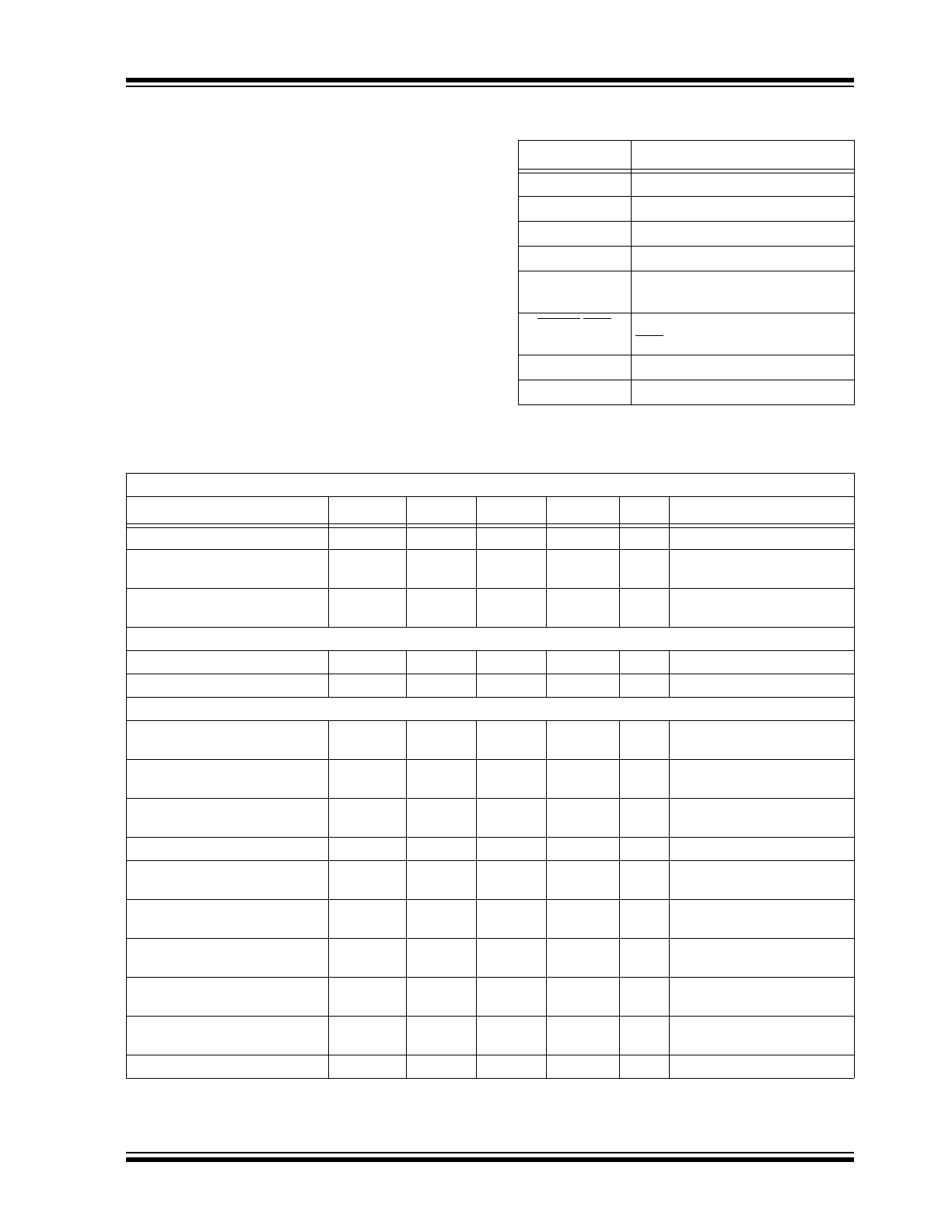
1.0
ELECTRICAL
CHARACTERISTICS
Absolute Maximum Ratings†
Supply Voltage (V
DD
) .......................................................6.0V
Input Voltage, Any Pin................(GND - 0.3V) to (V
DD
+0.3V)
Operating Temperature Range ....................- 40°C to +125°C
Maximum Junction Temperature, T
J
........................... +150°C
ESD Protection on all pins ........................................... > 3 kV
† Notice: Stresses above those listed under “Maximum
Ratings” may cause permanent damage to the device. This is
a stress rating only and functional operation of the device at
those or any other conditions above those indicated in the
operational listings of this specification is not implied. Expo-
sure to maximum rating conditions for extended periods may
affect device reliability.
PIN FUNCTION TABLE
Name
Function
V
IN
Analog Input
C
F
Analog Output
V
AS
Analog Input
GND
Ground
SENSE/NC
Analog Input.
No Connect (NC) for TC648B
FAULT/OTF
Digital (Open-Drain) Output
OTF for TC648B
V
OUT
Digital Output
V
DD
Power Supply Input
ELECTRICAL CHARACTERISTICS
Electrical Specifications: Unless otherwise specified, all limits are specified for -40°C < T
A
< +85°C, V
DD
= 3.0V to 5.5V.
Parameters
Sym
Min
Typ
Max
Units
Conditions
Supply Voltage
V
DD
3.0
—
5.5
V
Supply Current, Operating
I
DD
—
200
400
µA
Pins 6, 7 Open,
C
F
= 1 µF, V
IN
= V
C(MAX)
Supply Current, Shutdown Mode
I
DD(SHDN)
—
30
—
µA
Pins 6, 7 Open,
C
F
= 1 µF, V
IN
= 0.35V
V
OUT
Output
Sink Current at V
OUT
Output
I
OL
1.0
—
—
mA
V
OL
= 10% of V
DD
Source Current at V
OUT
Output
I
OH
5.0
—
—
mA
V
OH
= 80% of V
DD
V
IN
, V
AS
Inputs
Input Voltage at V
IN
for 100% PWM
Duty Cycle
V
C(MAX)
2.45
2.60
2.75
V
Over-Temperature Indication
Threshold
V
OTF
V
C(MAX)
+
20 mV
V
For TC646B and TC648B
Over-Temperature Indication
Threshold Hysteresis
V
OTF-HYS
80
mV
For TC646B and TC648B
V
C(MAX)
- V
C(MIN)
V
C(SPAN)
1.3
1.4
1.5
V
Hysteresis on Auto-Shutdown
Comparator
V
HAS
—
70
—
mV
Auto-Shutdown Threshold
V
AS
V
C(MAX)
-
V
C(SPAN)
—
V
C(MAX)
V
Voltage Applied to V
IN
to Ensure
Shutdown Mode
V
SHDN
—
—
V
DD
x 0.13
V
Voltage Applied to V
IN
to Release
Shutdown Mode
V
REL
V
DD
x 0.19
—
—
V
V
DD
= 5V
Hysteresis on V
SHDN
, V
REL
V
HYST
—
0.03 X
V
DD
—
V
V
IN
,
V
AS
Input Leakage
I
IN
- 1.0
—
+1.0
µA
Note 1
Note
1:
Ensured by design, tested during characterization.
2:
For V
DD
< 3.7V, t
STARTUP
and t
MP
timers are typically 13/f.
TC646B/TC648B/TC649B
DS21755C-page 4
2002-2013 Microchip Technology Inc.
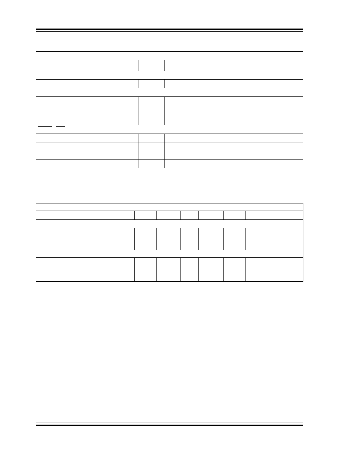
TEMPERATURE SPECIFICATIONS
Pulse-Width Modulator
PWM Frequency
f
PWM
26
30
34
Hz
C
F
= 1.0 µF
SENSE Input (TC646B & TC649B)
SENSE Input Threshold Voltage
with Respect to GND
V
TH(SENSE)
50
70
90
mV
Blanking time to ignore pulse due
to V
OUT
turn-on
t
BLANK
—
3.0
—
µsec
FAULT / OTF Output
Output Low Voltage
V
OL
—
—
0.3
V
I
OL
= 2.5 mA
Missing Pulse Detector Timer
t
MP
—
32/f
—
sec
TC646B and TC649B, Note 2
Start-up Timer
t
STARTUP
—
32/f
—
sec
Note 2
Diagnostic Timer
t
DIAG
—
3/f
—
sec
TC646B and TC649B
ELECTRICAL CHARACTERISTICS (CONTINUED)
Electrical Specifications: Unless otherwise specified, all limits are specified for -40°C < T
A
< +85°C, V
DD
= 3.0V to 5.5V.
Parameters
Sym
Min
Typ
Max
Units
Conditions
Note
1:
Ensured by design, tested during characterization.
2:
For V
DD
< 3.7V, t
STARTUP
and t
MP
timers are typically 13/f.
Electrical Characteristics: Unless otherwise noted, all parameters apply at V
DD
= 3.0V to 5.5V
Parameters
Sym
Min
Typ
Max
Units
Conditions
Temperature Ranges
Specified Temperature Range
T
A
-40
—
+85
°C
Operating Temperature Range
T
A
-40
—
+125
°C
Storage Temperature Range
T
A
-65
—
+150
°C
Thermal Package Resistances
Thermal Package Resistance, 8-Pin MSOP
JA
—
200
—
°C/W
Thermal Package Resistance, 8-Pin SOIC
JA
—
155
—
°C/W
Thermal Package Resistance, 8-Pin PDIP
JA
—
125
—
°C/W
2002-2013 Microchip Technology Inc.
DS21755C-page 5
TC646B/TC648B/TC649B
TIMING SPECIFICATIONS
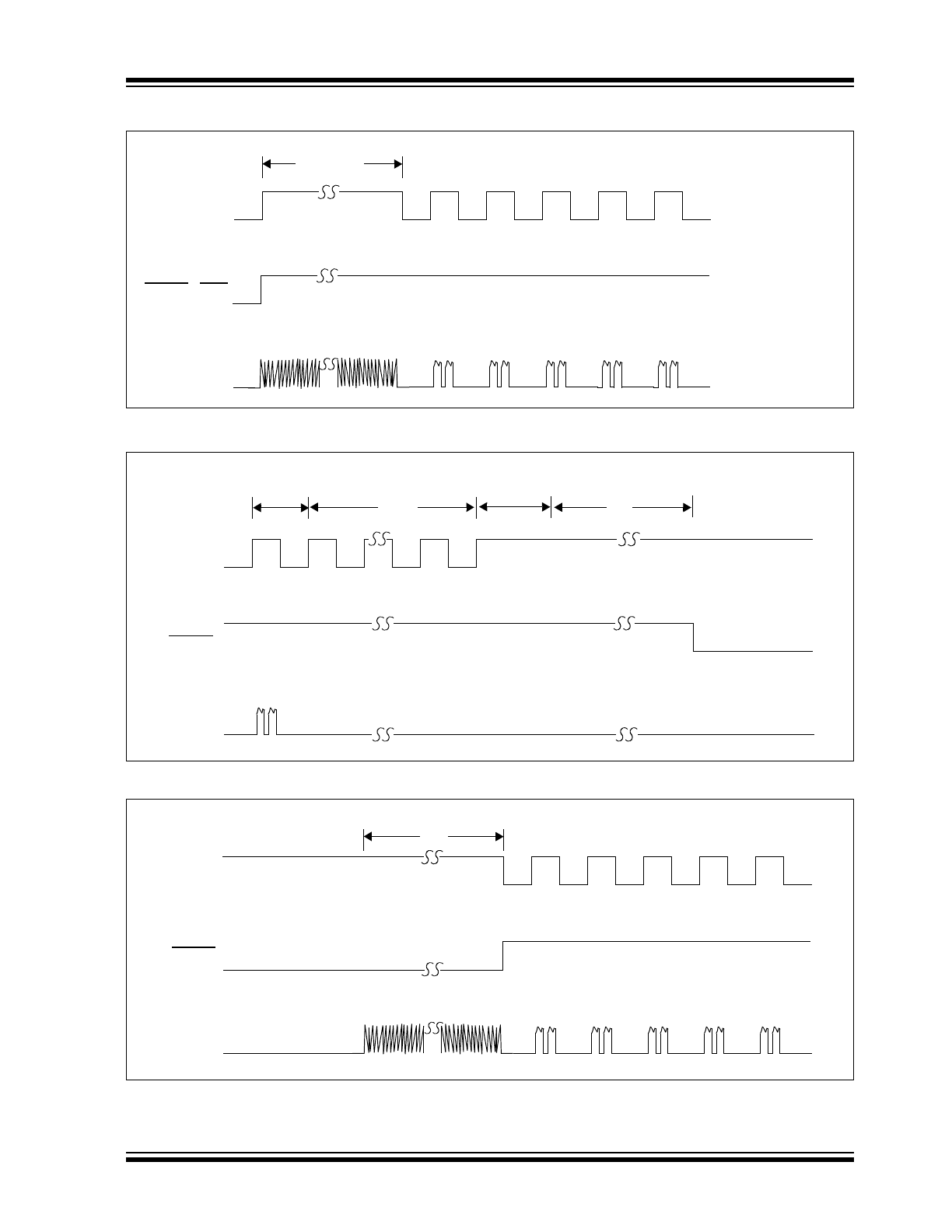
FIGURE 1-1:
TC646B/TC648B/TC649B Start-up Timing.
FIGURE 1-2:
Fan Fault Occurrence (TC646B and TC649B).
FIGURE 1-3:
Recovery From Fan Fault (TC646B and TC649B).
V
OUT
FAULT / OTF
SENSE
t
STARTUP
(TC646B and TC649B)
V
OUT
FAULT
SENSE
33.3 msec (C
F
= 1 µF)
t
MP
t
MP
t
DIAG
V
OUT
FAULT
SENSE
Minimum 16 pulses
t
MP
TC646B/TC648B/TC649B
DS21755C-page 6
2002-2013 Microchip Technology Inc.
FIGURE 1-4:
TC646B/TC648B/TC649B Electrical Characteristics Test Circuit.
1
2
3
4
6
5
7
8
V
IN
C
F
V
AS
GND
FAULT / OTF
SENSE
V
OUT
V
DD
R
3
R
1
C
3
0.1 µF
C
2
1 µF
V
DD
C
1
0.1 µF
+
-
V
IN
+
-
C
4
0.1 µF
V
AS
+
-
R
2
K
1
K
2
0.1 µF
1 µF
.01 µF
C
7
C
6
C
5
R
4
V
SENSE
(pulse voltage source)
K
4
K
3
+
-
Current
limited
voltage
source
V
DD
R
5
Current
limited
voltage
source
C
8
0.1 µF
R
6
Note: C
5
and C
7
are adjusted to get the necessary 1 µF value.
TC646B and TC649B
TC646B
TC648B
TC649B
+
-
2002-2013 Microchip Technology Inc.
DS21755C-page 7
TC646B/TC648B/TC649B
2.0
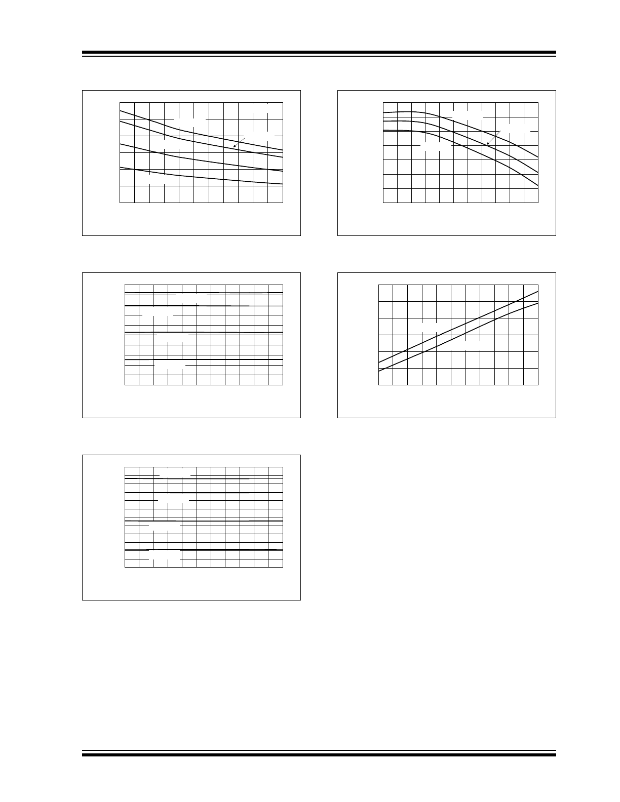
TYPICAL PERFORMANCE CURVES
Note: Unless otherwise indicated, V
DD
= 5V, T
A
= 25°C.
FIGURE 2-1:
I
DD
vs. Temperature.
FIGURE 2-2:
PWM Sink Current (I
OL
) vs.
V
OL
.
FIGURE 2-3:
PWM Source Current (I
OH
)
vs. V
DD
- V
OH
.
FIGURE 2-4:
PWM Frequency vs.
Temperature.
FIGURE 2-5:
I
DD
vs. V
DD
.
FIGURE 2-6:
I
DD
Shutdown vs.
Temperature.
Note:
The graphs and tables provided following this note are a statistical summary based on a limited number of
samples and are provided for informational purposes only. The performance characteristics listed herein
are not tested or guaranteed. In some graphs or tables, the data presented may be outside the specified
operating range (e.g., outside specified power supply range) and therefore outside the warranted range.
125
130
135
140
145
150
155
160
165
-40
-25
-10
5
20
35
50
65
80
95
110 125
Temperature (ºC)
I
DD
(µA
)
V
DD
= 3.0V
V
DD
= 5.5V
Pins 6 & 7 Open
C
F
= 1 µF
0
2
4
6
8
10
12
14
16
0
50
100 150 200 250 300 350 400 450 500 550 600
V
OL
(mV)
I
OL
(m
A
)
V
DD
= 5.5V
V
DD
= 5.0V
V
DD
= 3.0V
V
DD
= 4.0V
0
2
4
6
8
10
12
14
16
0
100
200
300
400
500
600
700
800
V
DD
- V
OH
(mV)
I
OH
(m
A
)
V
DD
= 5.5V
V
DD
= 5.0V
V
DD
= 3.0V
V
DD
= 4.0V
28.50
29.00
29.50
30.00
30.50
-40 -25 -10
5
20
35
50
65
80
95 110 125
Temperature (ºC)
Oscillator Frequency (Hz)
V
DD
= 3.0V
V
DD
= 5.5V
C
F
= 1.0PF
125
130
135
140
145
150
155
160
165
170
3
3.5
4
4.5
5
5.5
V
DD
(V)
I
DD
(µA
)
T
A
= -40ºC
T
A
= -5ºC
T
A
= +125ºC
T
A
= +90ºC
Pins 6 & 7 Open
C
F
= 1 µF
15
18
21
24
27
30
-40
-25
-10
5
20
35
50
65
80
95
110 125
Temperature (ºC)
I
DD
S
hutdow
n (µA
)
V
DD
= 5.5V
V
DD
= 3.0V
Pins 6 & 7 Open
V
IN
= 0V
TC646B/TC648B/TC649B
DS21755C-page 8
2002-2013 Microchip Technology Inc.
Note: Unless otherwise indicated, V
DD
= 5V, T
A
= 25°C.
FIGURE 2-7:
FAULT / OTF V
OL
vs.
Temperature.
FIGURE 2-8:
V
C(MAX)
vs. Temperature.
FIGURE 2-9:
V
C(MIN)
vs. Temperature.
FIGURE 2-10:
Sense Threshold
(V
TH(SENSE)
) vs. Temperature.
FIGURE 2-11:
FAULT / OTF I
OL
vs. V
OL
.
FIGURE 2-12:
PWM Source Current (I
OH
)
vs. Temperature.
10
20
30
40
50
60
70
-40
-25
-10
5
20
35
50
65
80
95
110 125
Temperature (ºC)
FA
U
LT /
OTF V
OL
(mV)
I
OL
= 2.5 mA
V
DD
= 3.0V
V
DD
= 5.5V
V
DD
= 5.0V
V
DD
= 4.0V
2.570
2.580
2.590
2.600
2.610
-40
-25
-10
5
20
35
50
65
80
95
110 125
Temperature (ºC)
V
C(M
A
X)
(V
)
V
DD
= 5.0V
V
DD
= 5.5V
V
DD
= 3.0V
C
F
= 1 µF
1.180
1.190
1.200
1.210
1.220
-40
-25
-10
5
20
35
50
65
80
95
110 125
Temperature (ºC)
V
C(M
IN)
(V
)
V
DD
= 5.0V
V
DD
= 3.0V
C
F
= 1 µF
69.5
70.0
70.5
71.0
71.5
72.0
72.5
73.0
73.5
74.0
-40
-25
-10
5
20
35
50
65
80
95
110 125
Temperature (ºC)
V
TH(SENSE)
(m
V
)
V
DD
= 3.0V
V
DD
= 4.0V
V
DD
= 5.5V
V
DD
= 5.0V
0
2
4
6
8
10
12
14
16
18
20
22
0
50
100
150
200
250
300
350
400
V
OL
(mV)
FA
U
LT /
O
TF I
OL
(m
A
)
V
DD
= 5.5V
V
DD
= 3.0V
V
DD
= 4.0V
V
DD
= 5.0V
5.00
10.00
15.00
20.00
25.00
30.00
35.00
40.00
45.00
-40
-25
-10
5
20
35
50
65
80
95
110 125
Temperature (ºC)
V
OUT
I
OH
(m
A
)
V
DD
= 5.5V
V
DD
= 5.0V
V
DD
= 4.0V
V
DD
= 3.0V
V
OH
= 0.8V
DD
2002-2013 Microchip Technology Inc.
DS21755C-page 9
TC646B/TC648B/TC649B
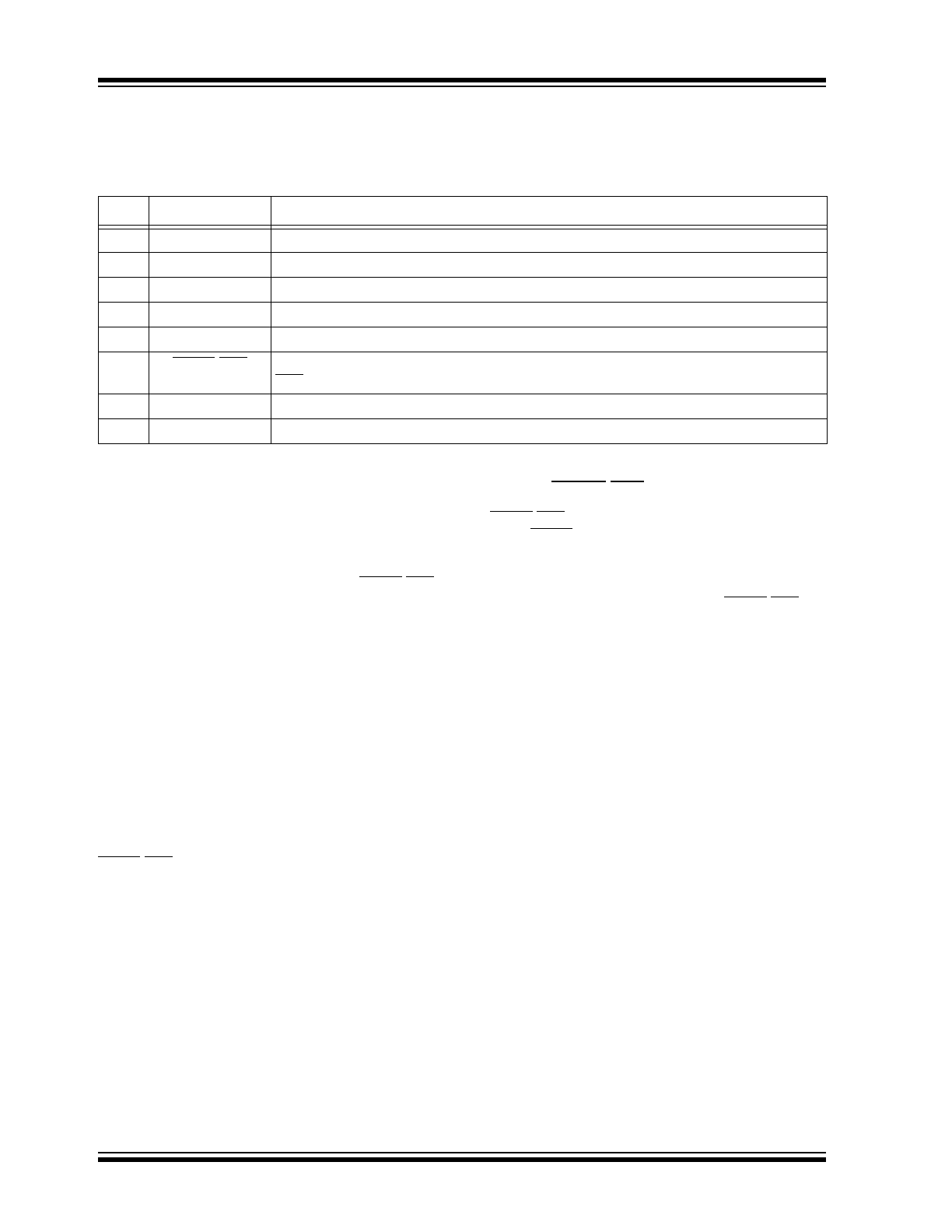
Note: Unless otherwise indicated, V
DD
= 5V, T
A
= 25°C.
FIGURE 2-13:
PWM Sink Current (I
OL
) vs.
Temperature.
FIGURE 2-14:
V
SHDN
Threshold vs.
Temperature.
FIGURE 2-15:
V
REL
Threshold vs.
Temperature.
FIGURE 2-16:
V
OTF
Threshold vs.
Temperature.
FIGURE 2-17:
Over-Temperature
Hysteresis (V
OTF-HYS
) vs. Temperature.
0
5
10
15
20
25
30
-40
-25
-10
5
20
35
50
65
80
95
110 125
Temperature (ºC)
V
OUT
I
OL
(m
A
)
V
DD
= 5.5V
V
DD
= 5.0V
V
DD
= 4.0V
V
DD
= 3.0V
V
OL
= 0.1V
DD
0.30
0.35
0.40
0.45
0.50
0.55
0.60
0.65
0.70
0.75
0.80
-40
-25
-10
5
20
35
50
65
80
95
110 125
Temperature (ºC)
V
SHDN
(V
)
V
DD
= 3.0V
V
DD
= 4.0V
V
DD
= 5.0V
V
DD
= 5.5V
0.40
0.45
0.50
0.55
0.60
0.65
0.70
0.75
0.80
0.85
0.90
0.95
1.00
-40
-25
-10
5
20
35
50
65
80
95
110 125
Temperature (ºC)
V
REL
(V
)
V
DD
= 3.0V
V
DD
= 4.0V
V
DD
= 5.0V
V
DD
= 5.5V
2.595
2.600
2.605
2.610
2.615
2.620
2.625
2.630
-40
-25
-10
5
20
35
50
65
80
95
110 125
Temperature (ºC)
V
OT
F
(V
)
V
DD
= 3.0V
V
DD
= 5.0V
V
DD
= 5.5V
70
75
80
85
90
95
100
-40
-25
-10
5
20
35
50
65
80
95
110 125
Temperature (ºC)
V
OT
F
H
yster
esis (m
V
)
V
DD
= 5.5V
V
DD
= 3.0V
TC646B/TC648B/TC649B
DS21755C-page 10
2002-2013 Microchip Technology Inc.
3.0
PIN FUNCTIONS
The descriptions of the pins are given in Table 3-1.
TABLE 3-1:
PIN FUNCTION TABLE
3.1
Analog Input (V
IN
)
The thermistor network (or other temperature sensor)
connects to V
IN
. A voltage range of 1.20V to 2.60V (typ-
ical) on this pin drives an active duty cycle of 0% to
100% on the V
OUT
pin. The TC646B, TC648B and
TC649B devices enter shutdown mode when
0
V
IN
V
SHDN
. During shutdown, the FAULT/OTF
output is inactive and supply current falls to 30 µA
(typical).
3.2
Analog Output (C
F
)
C
F
is the positive terminal for the PWM ramp generator
timing capacitor. The recommended value for the C
F
capacitor is 1.0 µF for 30 Hz PWM operation.
3.3
Analog Input (V
AS
)
An external resistor divider connected to V
AS
sets the
auto-shutdown threshold. Auto-shutdown occurs when
V
IN
< V
AS
. The fan is automatically restarted when
V
IN
> (V
AS
+ V
HAS
). During auto-shutdown, the
FAULT/OTF output is inactive and supply current falls
to 30 µA (typical).
3.4
Analog Input (SENSE)
Pulses are detected at SENSE as fan rotation chops
the current through a sense resistor. The absence of
pulses indicates a fan fault condition.
3.5
Digital (Open-Drain) Output
(FAULT/OTF)
FAULT/OTF goes low to indicate a fault condition.
When FAULT goes low due to a fan fault (TC646B and
TC649B devices), the output will remain low until the
fan fault condition has been removed (16 pulses have
been detected at the SENSE pin in a 32/f period). For
the TC646B and TC648B devices, the FAULT/OTF out-
put will also be asserted when the V
IN
voltage reaches
the V
OTF
threshold of 2.62V (typical). This gives an
over-temperature/100% fan speed indication
.
3.6
Digital Output (V
OUT
)
V
OUT
is an active-high complimentary output that
drives the base of an external NPN transistor (via an
appropriate base resistor) or the gate of an N-channel
MOSFET. This output has asymmetrical drive. During a
fan fault condition, the V
OUT
output is continuously on.
3.7
Power Supply Input (V
DD
)
The V
DD
pin with respect to GND provides power to the
device. This bias supply voltage may be independent of
the fan power supply.
3.8
Ground (GND)
Ground terminal.
3.9
No Connect (NC)
No internal connection.
Pin
Name
Function
1
V
IN
Analog Input
2
C
F
Analog Output
3
V
AS
Analog Input
4
GND
Ground
5
SENSE/NC
Analog Input/No Connect. NC for TC648B.
6
FAULT/OTF
Digital (Open-Drain) Output
OTF for TC648B
7
V
OUT
Digital Output
8
V
DD
Power Supply Input