
2002-2014 Microchip Technology Inc.
DS20001734C-page 1
TC654/TC655
Features:
• Temperature Proportional Fan Speed for Reduced
Acoustic Noise and Longer Fan Life
• FanSense™ Protects against Fan Failure and
Eliminates the Need for 3-wire Fans
• Overtemperature Detection (TC655)
• Efficient PWM Fan Drive
• Provides RPM Data
• 2-Wire SMBus™-Compatible Interface
• Supports Any Fan Voltage
• Software Controlled Shutdown Mode for "Green"
Systems
• Supports Low-Cost NTC/PTC Thermistors
• Space Saving 10-Pin MSOP Package
• Temperature Range: -40°C to +85ºC
Applications:
• Personal Computers and Servers
• LCD Projectors
• Datacom and Telecom Equipment
• Fan Trays
• File Servers
• Workstations
• General Purpose Fan Speed Control
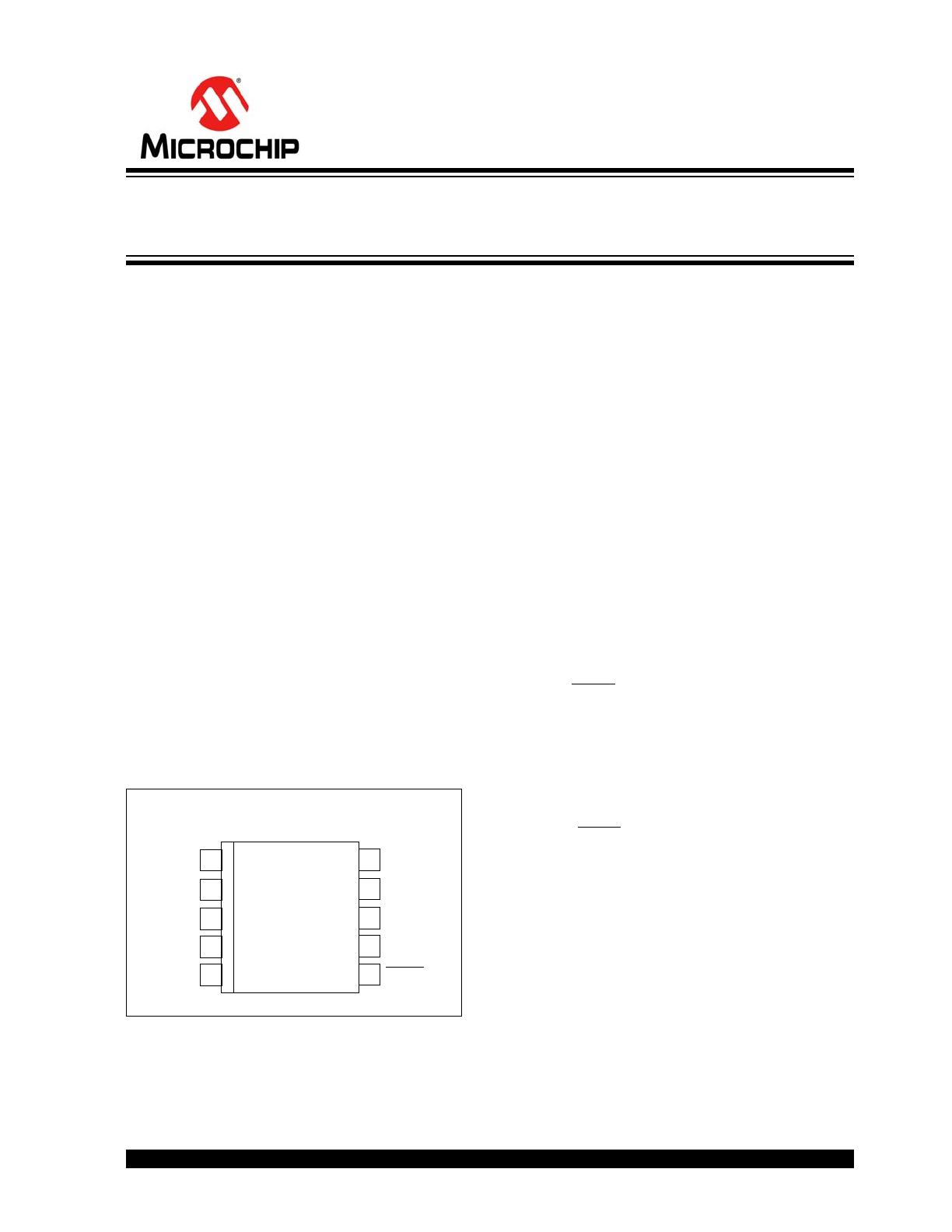
Package Type
Description:
The TC654 and TC655 are PWM mode fan speed con-
trollers with FanSense technology for use with brush-
less DC fans. These devices implement temperature
proportional fan speed control which lowers acoustic
fan noise and increases fan life. The voltage at V
IN
(Pin 1) represents temperature and is typically pro-
vided by an external thermistor or voltage output tem-
perature sensor. The PWM output (V
OUT
) is adjusted
between 30% and 100%, based on the voltage at V
IN
.
The PWM duty cycle can also be programmed via
SMBus to allow fan speed control without the need for
an external thermistor. If V
IN
is not connected, the
TC654/TC655 will start driving the fan at a default duty
cycle of 39.33%. See
Section 4.3 “Fan Start-up”
for
more details.
In normal fan operation, pulse trains are present at
SENSE1 (Pin 8) and SENSE2 (Pin 7). The TC654/
TC655 use these pulses to calculate the fan revolu-
tions per minute (RPM). The fan RPM data is used to
detect a worn out, stalled, open or unconnected fan.
An RPM level below the user-programmable threshold
causes the TC654/TC655 to assert a logic low alert
signal (FAULT). The default threshold value is
500 RPM. Also, if this condition occurs, F1F (bit 0<0>)
or F2F (bit 1<0>) in the Status Register will also be set
to a ‘1’.
An over-temperature condition is indicated when the
voltage at V
IN
exceeds 2.6V (typical). The TC654/
TC655 devices indicate this by setting OTF(bit 5<X>) in
the Status Register to a '1'. The TC655 device also
pulls the FAULT line low during an over-temperature
condition.
The TC654/TC655 devices are available in a 10-Pin
MSOP package and consume 150 µA during opera-
tion. The devices can also enter a low-power Shutdown
mode (5 µA, typ.) by setting the appropriate bit in the
Configuration Register. The operating temperature
range for these devices is -40°C to +85ºC.
10-Pin MSOP
1
2
3
4
5
10
9
8
7
6
V
IN
C
F
SCLK
SDA
GND
V
DD
V
OUT
SENSE1
SENSE2
FAULT
TC654
TC655
Dual SMBus™ PWM Fan Speed Controllers With
Fan Fault Detection
TC654/TC655
DS20001734C-page 2
2002-2014 Microchip Technology Inc.
Functional Block Diagram
V
OTF
50 k
OTF
V
MIN
TC654/TC655
SENSE1
FAULT
V
OUT
V
DD
GND
SDA
SCLK
C
F
V
IN
–
+
+
–
Clock
Generator
Serial Port
Interface
Control
Logic
Start-up
Timer
Missing
Pulse
Detect
100 mV (typ.)
–
50 k
SENSE2
100 mV (typ.)
–
–
+
Note: OTF condition applies for the TC655 device only.
Note
2002-2014 Microchip Technology Inc.
DS20001734C-page 3
TC654/TC655
1.0
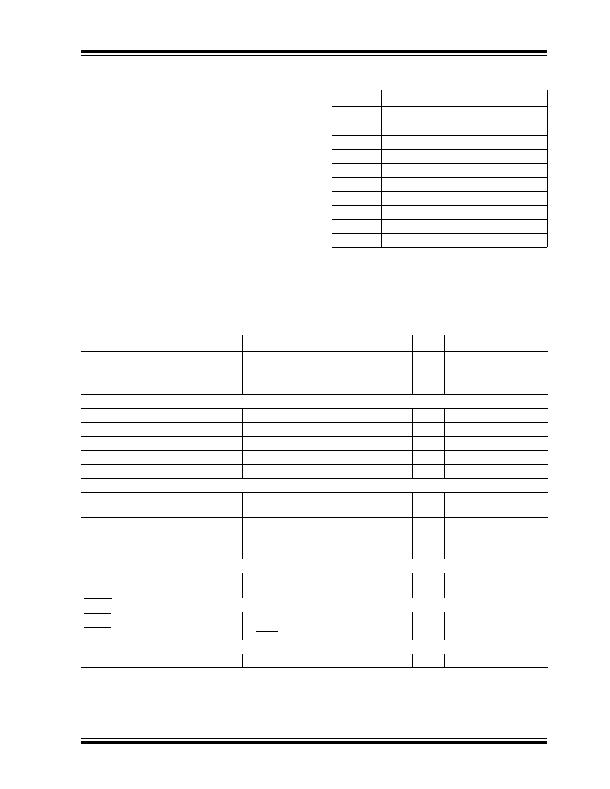
ELECTRICAL
CHARACTERISTICS
Absolute Maximum Ratings *
V
DD
...................................................................................6.5V
Input Voltages ...................................... -0.3V to (V
DD
+ 0.3V)
Output Voltages .................................... -0.3V to (V
DD
+ 0.3V)
Storage temperature .....................................-65°C to +150°C
Ambient temp. with power applied ................-40°C to +125°C
Maximum Junction Temperature, T
J
............................. 150°C
ESD protection on all pins
4 kV
*Notice: Stresses above those listed under “Maximum rat-
ings” may cause permanent damage to the device. This is a
stress rating only and functional operation of the device at
those or any other conditions above those indicated in the
operational listings of this specification is not implied. Expo-
sure to maximum rating conditions for extended periods may
affect device reliability.
PIN FUNCTION TABLE
Name
Function
V
IN
Analog Input
C
F
Analog Output
SCLK
Serial Clock Input
SDA
Serial Data In/Out (Open Drain)
GND
Ground
FAULT
Digital (Open Drain) Output
SENSE2
Analog Input
SENSE1
Analog Input
V
OUT
Digital Output
V
DD
Power Supply Input
ELECTRICAL SPECIFICATIONS
Electrical Characteristics: Unless otherwise noted, all limits are specified for V
DD
= 3.0V to 5.5V,
-40°C <T
A
< +85°C.
Parameters
Sym.
Min.
Typ.
Max.
Units
Conditions
Supply Voltage
V
DD
3.0
—
5.5
V
Operating Supply Current
I
DD
—
150
300
µA
Pins 7, 8, 9 Open
Shutdown Mode Supply Current
I
DDSHDN
—
5
10
µA
Pins 7, 8, 9 Open
V
OUT
PWM Output
V
OUT
Rise Time
t
R
—
—
50
µsec
I
OH
= 5 mA,
Note 1
V
OUT
Fall Time
t
F
—
—
50
µsec
I
OL
= 1 mA,
Note 1
Sink Current at V
OUT
Output
I
OL
1.0
—
—
mA
V
OL
= 10% of V
DD
Source Current at V
OUT
Output
I
OH
5.0
—
—
mA
V
OH
= 80% of V
DD
PWM Frequency
F
26
30
34
Hz
C
F
= 1 µF
V
IN
Input
V
IN
Input Voltage for 100% PWM
duty-cycle
V
C(MAX)
2.45
2.6
2.75
V
V
C(MAX)
- V
C(MIN)
V
CRANGE
1.25
1.4
1.55
V
V
IN
Input Resistance
—
10M
—
V
DD
= 5.0V
V
IN
Input Leakage Current
I
IN
-1.0
—
+1.0
µA
SENSE Input
SENSE Input Threshold Voltage with
Respect to GND
V
THSENSE
80
100
120
mV
FAULT Output
FAULT Output LOW Voltage
V
OL
—
—
0.3
V
I
OL
= 2.5 mA
FAULT Output Response Time
t
FAULT
—
2.4
—
sec
Fan RPM-to-Digital Output
Fan RPM ERROR
-15
—
+15
%
RPM > 1600
Note 1: Not production tested, ensured by design, tested during characterization.
2: For 5.0V > V
DD
5.5V, the limit for V
IH
= 2.2V.
TC654/TC655
DS20001734C-page 4
2002-2014 Microchip Technology Inc.
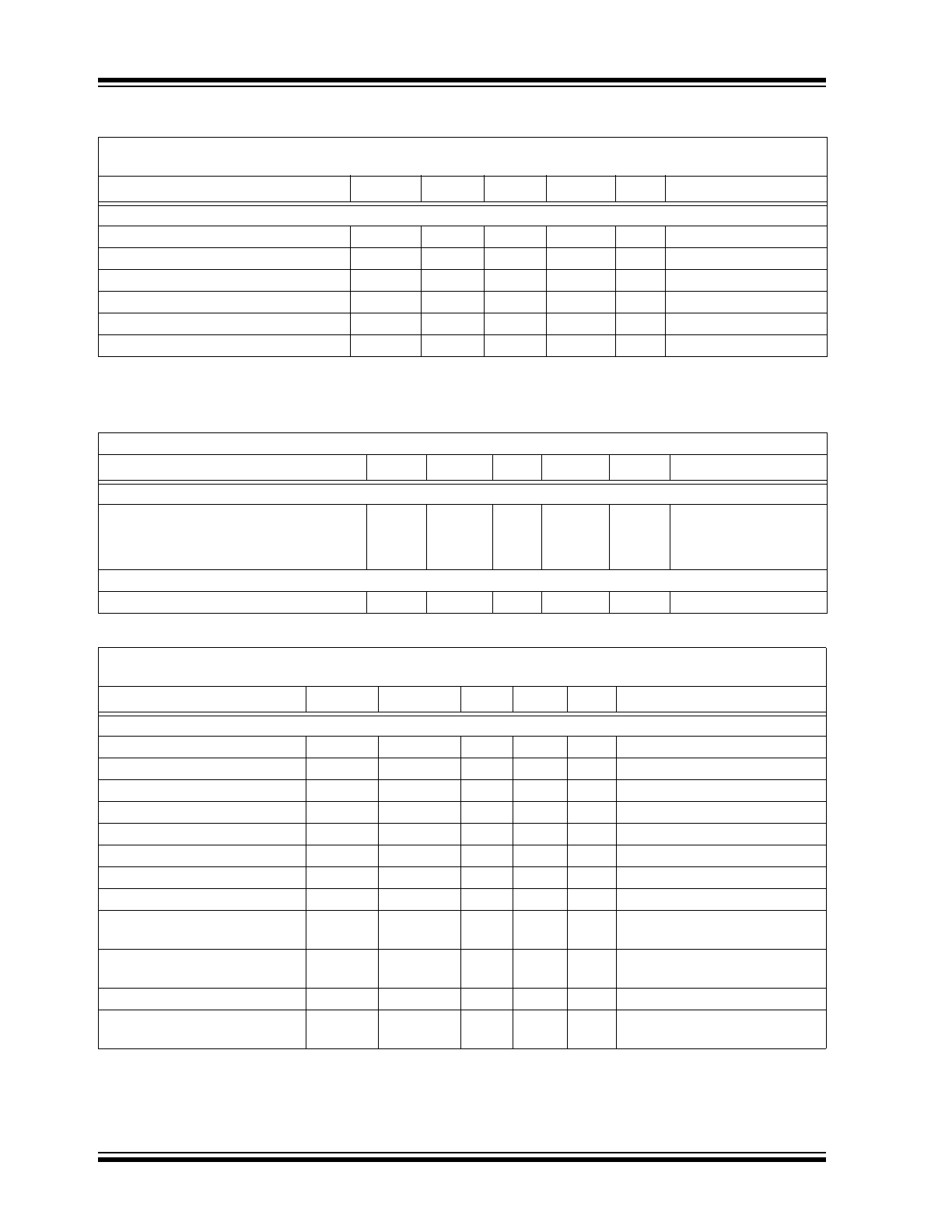
TEMPERATURE SPECIFICATIONS
TIMING SPECIFICATIONS
2-Wire Serial Bus Interface
Logic Input High
V
IH
2.1
—
—
V
Note 2
Logic Input Low
V
IL
—
—
0.8
V
Logic Output Low
V
OL
—
—
0.4
V
I
OL
= 3 mA
Input Capacitance SDA, SCLK
C
IN
—
10
15
pF
Note 1
I/O Leakage Current
I
LEAK
-1.0
—
+1.0
µA
SDA Output Low Current
I
OLSDA
6
—
—
mA
V
OL
= 0.6V
Electrical Characteristics: Unless otherwise noted, all parameters apply at V
DD
= 3.0 V to 5.5 V
Parameters
Symbol
Min
Typ
Max
Units
Conditions
Temperature Ranges
Specified Temperature Range
T
A
-40
—
+85
°C
Operating Temperature Range
T
A
-40
—
+125
°C
Storage Temperature Range
T
A
-65
—
+150
°C
Thermal Package Resistances
Thermal Resistance, 10 Pin MSOP
JA
—
113
—
°C/W
Electrical Characteristics: Unless otherwise noted, all limits are specified for V
DD
= 3.0V to 5.5V,
-40°C <T
A
< +85°C
Parameters
Sym
Min
Typ
Max
Units
Conditions
SMBus Interface (See
Figure 1-1
)
Serial Port Frequency
f
SC
0
—
100
kHz
Note 1
Low Clock Period
t
LOW
4.7
—
—
µsec
Note 1
High Clock Period
t
HIGH
4.7
—
—
µsec
Note 1
SCLK and SDA Rise Time
t
R
—
—
1000
nsec
Note 1
SCLK and SDA Fall Time
t
F
—
—
300
nsec
Note 1
Start Condition Setup Time
t
SU(START)
4.7
—
—
µsec
Note 1
SCLK Clock Period Time
t
SC
10
—
—
µsec
Note 1
Start Condition Hold Time
t
H(START)
4.0
—
—
µsec
Note 1
Data in SetupTime to SCLK
High
t
SU-DATA
250
—
—
nsec
Note 1
Data in Hold Time after SCLK
Low
t
H-DATA
300
—
—
nsec
Note 1
Stop Condition Setup Time
t
SU(STOP)
4.0
—
—
µsec
Note 1
Bus Free Time Prior to New
Transition
t
IDLE
4.7
—
µsec
Note 1
and
Note 2
Note 1: Not production tested, ensured by design, tested during characterization.
2: Time the bus must be free before a new transmission can start.
ELECTRICAL SPECIFICATIONS (CONTINUED)
Electrical Characteristics: Unless otherwise noted, all limits are specified for V
DD
= 3.0V to 5.5V,
-40°C <T
A
< +85°C.
Parameters
Sym.
Min.
Typ.
Max.
Units
Conditions
Note 1: Not production tested, ensured by design, tested during characterization.
2: For 5.0V > V
DD
5.5V, the limit for V
IH
= 2.2V.
2002-2014 Microchip Technology Inc.
DS20001734C-page 5
TC654/TC655
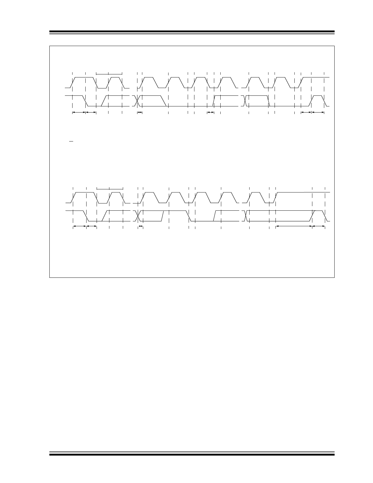
FIGURE 1-1:
Bus Timing Data.
t
SU(START)
t
H(START)
t
SU-DATA
t
SU(STOP)
t
IDLE
A = Start Condition
B = MSB of Address Clocked into Slave
C = LSB of Address Clocked into Slave
D = R/W Bit Clocked into Slave
E = Slave Pulls SDA Line Low
A
B
C
D
E
F
G
H
I
J
K
L
M
F = Acknowledge Bit Clocked into Master
G = MSB of Data Clocked into Slave
H = LSB of Data Clocked into Slave
I = Slave Pulls SDA Line Low
J = Acknowledge Clocked into Master
K = Acknowledge Clock Pulse
L = Stop Condition, Data Executed by Slave
M = New Start Condition
t
LOW
t
HIGH
SCLK
SDA
t
H-DATA
SMBus Write Timing Diagram
t
SU(START)
t
H(START)
t
SU-DATA
t
SU(STOP)
t
IDLE
A = Start Condition
B = MSB of Address Clocked into Slave
C = LSB of Address Clocked into Slave
D = R/W Bit Clocked into Slave
A
B
C
D
E F
G
H
I
J
K
E = Slave Pulls SDA Line Low
F = Acknowledge Bit Clocked into Master
G = MSB of Data Clocked into Master
H = LSB of Data Clocked into Master
t
LOW
t
HIGH
I = Acknowledge Clock Pulse
J = Stop Condition
K = New Start Condition
SCLK
SDA
SMBus Read Timing Diagram
E
TC654/TC655
DS20001734C-page 6
2002-2014 Microchip Technology Inc.
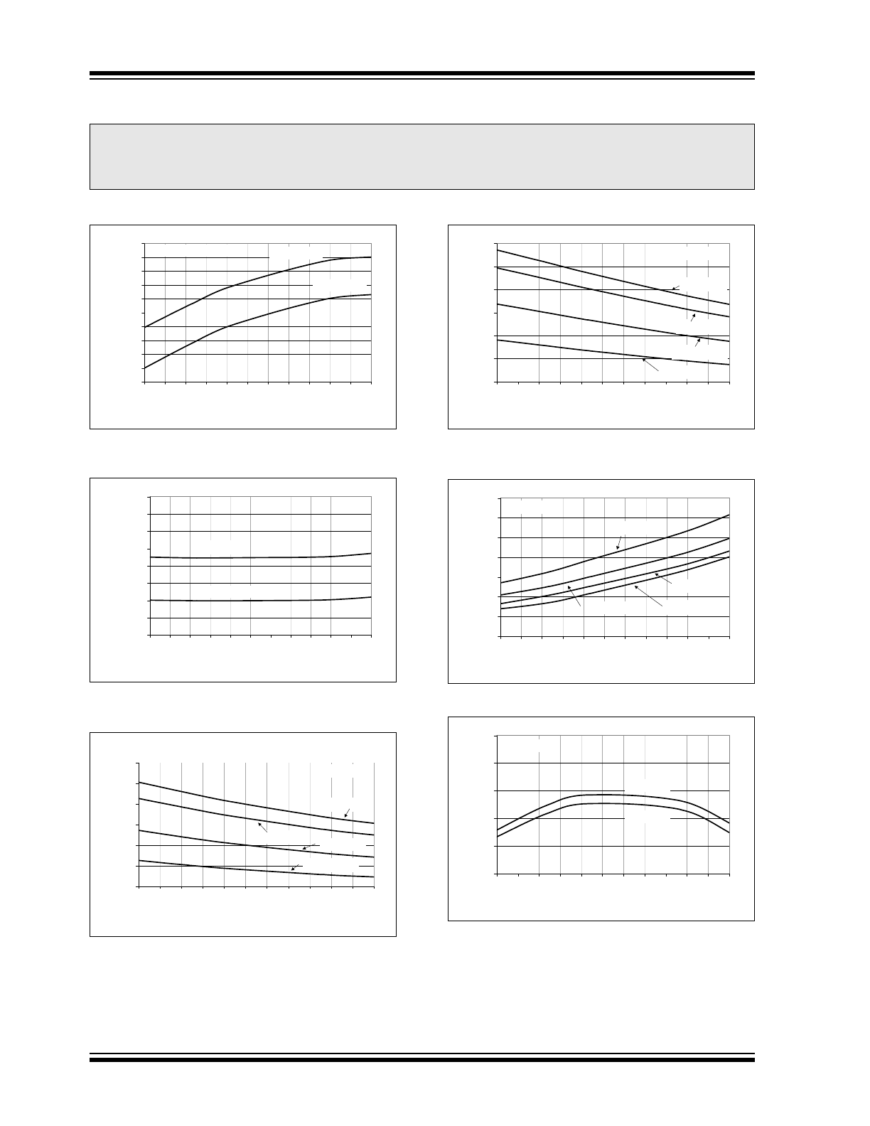
2.0
TYPICAL PERFORMANCE CURVES
FIGURE 2-1:
I
DD
vs. Temperature.
FIGURE 2-2:
I
DD
Shutdown vs.
Temperature.
FIGURE 2-3:
PWM, Source Current vs.
Temperature.
FIGURE 2-4:
PWM, Sink Current vs.
Temperature.
FIGURE 2-5:
Fault V
OL
vs. Temperature.
FIGURE 2-6:
PWM Frequency vs.
Temperature.
Note:
The graphs and tables provided following this note are a statistical summary based on a limited number of
samples and are provided for informational purposes only. The performance characteristics listed herein
are not tested or guaranteed. In some graphs or tables, the data presented may be outside the specified
operating range (e.g., outside specified power supply range) and therefore outside the warranted range.
130
135
140
145
150
155
160
165
170
175
180
-40
-25
-10
5
20
35
50
65
80
95
110 125
Temperature (°C)
I
DD
(µA
)
V
DD
= 5.5 V
V
DD
= 3.0 V
Pins 7,8, and 9 Open
1.000
2.000
3.000
4.000
5.000
6.000
7.000
8.000
9.000
-40
-25
-10
5
20
35
50
65
80
95
110 125
Temperature (ºC)
S
hutdow
n I
DD
(µA
)
V
DD
= 3.0 V
V
DD
= 5.5 V
5
10
15
20
25
30
35
-40
-25
-10
5
20
35
50
65
80
95
110
125
Temperature (°C)
S
our
ce C
u
rr
e
nt (m
A
)
V
DD
= 5.5 V
V
DD
= 5.0 V
V
DD
= 4.0 V
V
DD
= 3.0 V
V
OH
= 0.8V
DD
2
4
6
8
10
12
14
-40
-25
-10
5
20
35
50
65
80
95
110 125
Temperature (°C)
S
ink C
u
rr
e
nt (m
A
)
V
DD
= 5.5 V
V
DD
= 5.0 V
V
DD
= 4.0 V
V
DD
= 3.0 V
V
OL
= 0.1 V
DD
15
20
25
30
35
40
45
50
-40
-25
-10
5
20
35
50
65
80
95
110 125
Temperature (ºC)
Faul
t V
OL
(m
V
)
I
OL
= 2.5 mA
V
DD
= 5.5 V
V
DD
= 5.0 V
V
DD
= 4.0 V
V
DD
= 3.0 V
27
28
29
30
31
32
-40
-25
-10
5
20
35
50
65
80
95
110 125
Temperature (ºC)
P
W
M Fr
equency (H
z
)
V
DD
= 5.5 V
V
DD
= 3.0 V
C
F
= 1.0 µF
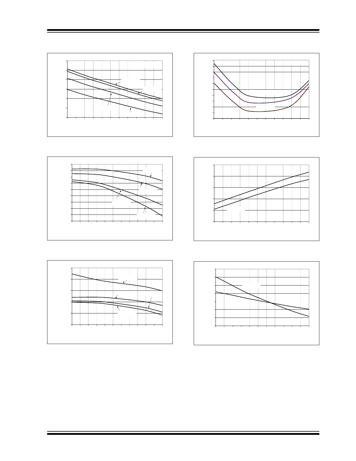
2002-2014 Microchip Technology Inc.
DS20001734C-page 7
TC654/TC655
FIGURE 2-7:
SDA I
OL
vs. Temperature.
FIGURE 2-8:
V
CMAX
vs. Temperature.
FIGURE 2-9:
V
CMIN
vs. Temperature.
FIGURE 2-10:
RPM %error vs.
Temperature.
FIGURE 2-11:
Sense Threshold
(V
THSENSE
) Hysteresis vs. Temperature.
FIGURE 2-12:
SDA, SCLK Hysteresis vs.
Temperature.
20
25
30
35
40
45
50
-40
-25
-10
5
20
35
50
65
80
95
110 125
Temperature (ºC)
SDA I
OL
(m
A
)
V
OL
= 0.4 V
V
DD
= 5.5 V
V
DD
= 5.0 V
V
DD
= 4.0 V
V
DD
= 3.0 V
2.575
2.580
2.585
2.590
2.595
2.600
2.605
2.610
2.615
2.620
-40
-25
-10
5
20
35
50
65
80
95
110 125
Temperature (ºC)
V
CM
a
x
(V
)
V
DD
= 3.0 V
V
DD
= 4.0 V
V
DD
= 5.0 V
V
DD
= 5.5 V
1.180
1.185
1.190
1.195
1.200
1.205
-40
-25
-10
5
20
35
50
65
80
95
110 125
Temperature (ºC)
V
CM
IN
(V
)
V
DD
= 3.0 V
V
DD
= 5.0 V
V
DD
= 5.5 V
V
DD
= 4.0 V
0
1
2
3
4
5
6
7
8
9
10
-40
-25
-10
5
20
35
50
65
80
95
110 125
Temperature (ºC)
R
P
M
Erro
r (
%
)
V
DD
= 3.0 V
V
DD
= 5.5 V
V
DD
= 5.0 V
C
F
= 1.0 µF
20
25
30
35
40
45
-40
-25
-10
5
20
35
50
65
80
95
110 125
Temperature (ºC)
V
THSENSE
H
yster
esis (m
V
)
V
DD
= 3.0V
V
DD
= 5.5V
80
90
100
110
120
130
140
150
-40
-25
-10
5
20
35
50
65
80
95
110 125
Temperature (ºC)
S
D
A
&
S
C
LK
H
yster
esis (m
V
)
V
DD
= 3.0 V
V
DD
= 5.0 V

TC654/TC655
DS20001734C-page 8
2002-2014 Microchip Technology Inc.
3.0
PIN FUNCTIONS
The descriptions of the pins are listed in
Table 3-1
.
TABLE 3-1:
PIN FUNCTION TABLE
3.1
Analog Input (V
IN
)
A voltage range of 1.62V to 2.6V (typical) on this pin
drives an active duty-cycle of 30% to 100% on the
V
OUT
pin.
3.2
Analog Output (C
F
)
Positive terminal for the PWM ramp generator timing
capacitor. The recommended C
F
is 1 µF for 30 Hz
PWM operation.
3.3
SMBus Serial Clock Input (SCLK)
Clocks data into and out of the TC654/TC655. See
Section 5.0 “Serial Communication”
for more infor-
mation on the serial interface.
3.4
Serial Data (Bi-directional) (SDA)
Serial data is transferred on the SMBus in both direc-
tions using this pin. See
Section 5.0 “Serial Commu-
nication”
for more information on the serial interface.
3.5
Digital (Open Drain) Output
(FAULT)
When the fan’s RPM falls below the user-set RPM
threshold (or OTF occurs with TC655), a logic low sig-
nal is asserted.
3.6
Analog Input (SENSE2)
Fan current pulses are detected at this pin. These
pulses are counted and used in the calculation of the
Fan 2 RPM.
3.7
Analog Input (SENSE1)
Fan current pulses are detected at this pin. These
pulses are counted and used in the calculation of the
Fan 1 RPM.
3.8
Digital Output (V
OUT
)
This active high complimentary output drives the base
of an external transistor or the gate of a MOSFET.
3.9
Power Supply Input (V
DD
)
The V
DD
pin with respect to GND provides power to the
device. This bias supply voltage may be independent of
the fan power supply.
Name
Function
V
IN
Analog Input
C
F
Analog Output
SCLK
Serial Clock Input
SDA
Serial Data In/Out (Open Drain)
GND
Ground
FAULT
Digital (Open Drain) Output
SENSE2
Analog Input
SENSE1
Analog Input
V
OUT
Digital Output
V
DD
Power Supply Input
2002-2014 Microchip Technology Inc.
DS20001734C-page 9
TC654/TC655
4.0
DEVICE OPERATION
The TC654 and TC655 devices allow you to control,
monitor and communicate (via SMBus) fan speed for 2-
wire and 3-wire DC brushless fans. By pulse-width
modulating (PWM) the voltage across the fan, the
TC654/TC655 controls fan speed according to the sys-
tem temperature.The goal of temperature proportional
fan speed control is to reduce fan power consumption,
increase fan life and reduce system acoustic noise.
With the TC654 and TC655 devices, fan speed can be
controlled by the analog input V
IN
or the SMBus inter-
face, allowing for high system flexibility.
The TC654 and TC655 also measure and monitor fan
revolutions per minute (RPM). A fan’s speed (RPM) is
a measure of its health. As a fan’s bearings wear out,
the fan slows down and eventually stops (locked rotor).
By monitoring the fan’s RPM level, the TC654/TC655
devices can detect open, shorted, unconnected and
locked rotor fan conditions. The fan speed threshold
can be set to provide a predictive fan failure feature.
This feature can be used to give a system warning and,
in many cases, help to avoid a system thermal shut-
down condition. The fan RPM data and threshold reg-
isters are available over the SMBus interface which
allows for complete system control.
The TC654/TC655 devices are identical in every
aspect except for how they indicate an over-tempera-
ture condition. When V
IN
voltage exceeds 2.6V (typi-
cal), both devices will set OTF (bit 5<X>) in the Status
Register to a '1'. The TC655 will additionally pull the
FAULT output low during an over-temperature condi-
tion.
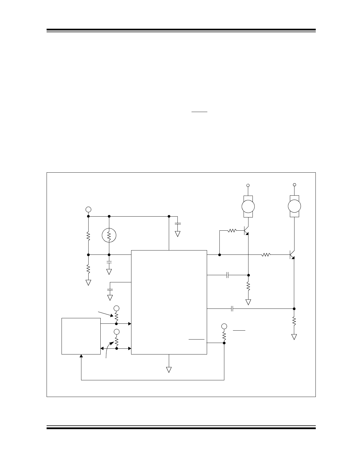
FIGURE 4-1:
Typical Application Circuit.
1
2
3
4
5
6
7
8
9
10
V
IN
C
F
SCLK
SDA
GND
FAULT
SENSE2
SENSE1
V
OUT
V
DD
+5V
FAN
FAN
R
ISO1
R
ISO2
R
SENSE2
R
SENSE1
C
SENSE2
C
SENSE1
1
2
NTC Thermistor
R
1
R
2
C
1
0.01 µF
C
2
1 µF
100 k
@ 25°C
PIC
®
Microcontroller
+12V
+5V
+5V
+5V
+5V
34.8 k
14.7 k
C
F
1.0 µF
R
SCLK
20 k
R
SDA
20 k
715
0.1 µF
0.1 µF
715
R
FAULT
20 k
Note: Refer to
Table 7-1
for R
SENSE1
and R
SENSE2
values.
TC654/TC655
TC654/TC655
DS20001734C-page 10
2002-2014 Microchip Technology Inc.
4.1
Fan Speed Control Methods
The speed of a DC brushless fan is proportional to the
voltage across it. For example, if a fan’s rating is
5000 RPM at 12V, it’s speed would be 2500 RPM at 6V.
This, of course, will not be exact, but should be close.
There are two main methods for fan speed control. The
first is pulse width modulation (PWM) and the second
is linear. Using either method the total system power
requirement to run the fan is equal. The difference
between the two methods is where the power is
consumed.
The following example compares the two methods for
a 12V, 120 mA fan running at 50% speed. With 6V
applied across the fan, the fan draws an average cur-
rent of 68 mA. Using a linear control method, there are
6V across the fan and 6V across the drive element.
With 6V and 68 mA, the drive element is dissipating
410 mW of power. Using the PWM approach, the fan is
modulated at a 50% duty cycle, with most of the 12V
being dropped across the fan. With 50% duty cycle, the
fan draws an RMS current of 110 mA and an average
current of 72 mA. Using a MOSFET with a 1
RDS
(on)
(a fairly typical value for this low current) the power dis-
sipation in the drive element would be: 12 mW (Irms
2
*
RDS
(on)
). Using a standard 2N2222A NPN transistor
(assuming a Vce-sat of 0.8V), the power dissipation
would be 58 mW (Iavg* Vce-sat).
The PWM approach to fan speed control causes much
less power dissipation in the drive element. This allows
smaller devices to be used and will not require any spe-
cial heatsinking to get rid of the power being dissipated
in the package.
The other advantage to the PWM approach is that the
voltage being applied to the fan is always near 12V.
This eliminates any concern about not supplying a high
enough voltage to run the internal fan components,
which is very relevant in linear fan speed control.
4.2
PWM Fan Speed Control
The TC654 and TC655 devices implement PWM fan
speed control by varying the duty cycle of a fixed fre-
quency pulse train. The duty cycle of a waveform is the
on time divided by the total period of the pulse. For
example, given a 100 Hz waveform (10 msec.) with an
on time of 5.0 msec, the duty cycle of this waveform is
50% (5.0 msec/10.0 msec). An example of this is
illustrated in
Figure 4-2
.
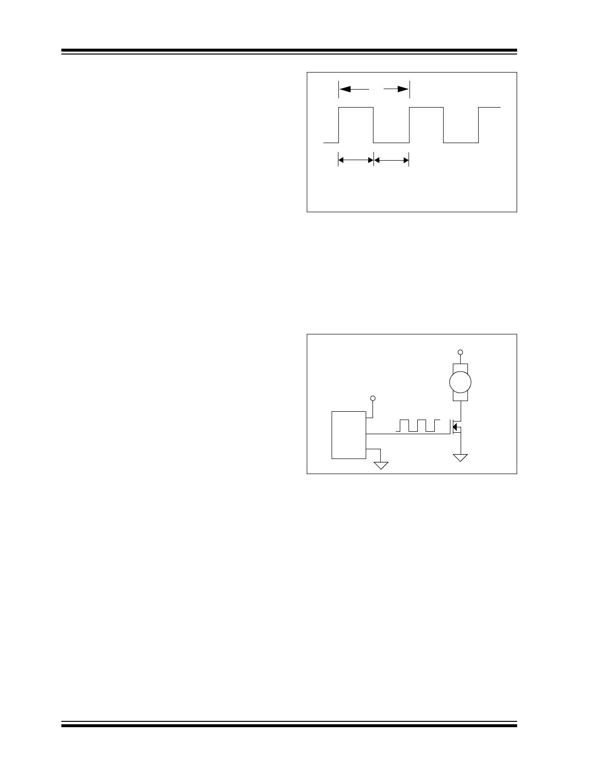
FIGURE 4-2:
Duty Cycle Of A PWM
Waveform.
The TC654 and TC655 generate a pulse train with a
typical frequency of 30 Hz (C
F
= 1 µF). The duty cycle
can be varied from 30% to 100%. The pulse train gen-
erated by the TC654/TC655 devices drives the gate of
an external N-channel MOSFET or the base of an NPN
transistor (
Figure 4-3
). See
Section 7.5 “Output Drive
Device Selection”
for more information on output
drive device selection.
FIGURE 4-3:
PWM Fan Drive.
By modulating the voltage applied to the gate of the
MOSFET Qdrive, the voltage applied to the fan is also
modulated. When the V
OUT
pulse is high, the gate of
the MOSFET is turned on, pulling the voltage at the
drain of Qdrive to 0V. This places the full 12V across
the fan for the Ton period of the pulse. When the duty
cycle of the drive pulse is 100% (full on, Ton = T), the
fan will run at full speed. As the duty cycle is decreased
(pulse on time “Ton” is lowered), the fan will slow down
proportionally. With the TC654 and TC655 devices, the
duty cycle can be controlled through the analog input
pin (V
IN
) or through the SMBus interface by using the
Duty-Cycle Register. See
Section 4.5 “Duty Cycle
Control (V
IN
and Duty-Cycle Register)”
for more
details on duty cycle control.
T
Ton
Toff
T = Period
T = 1/F
F = Frequency
D = Duty Cycle
D = Ton / T
TC654/
TC655
FAN
12V
Qdrive
V
DD
GND
V
OUT
G
D
S