
2002-2012 Microchip Technology Inc.
DS21712C-page 1
93LC46/56/66
Features:
• Single supply with programming operation down
to 2.5V
• Low-power CMOS technology
• 100
A typical active read current at 2.5V
• 3
A typical standby current at 2.5V
• ORG pin selectable memory configuration
• 128 x 8- or 64 x 16-bit organization (93LC46)
• 256 x 8- or 128 x 16-bit organization (93LC56)
• 512 x 8 or 256 x 16 bit organization (93LC66)
• Self-timed erase and write cycles
(including auto-erase)
• Automatic ERAL before WRAL
• Power on/off data protection circuitry
• Industry standard 3-wire serial I/O
• Device status signal during erase/write cycles
• Sequential read function
• 1,000,000 E/W cycles ensured
• Data retention > 200 years
• 8-pin PDIP/SOIC
(SOIC in JEDEC standards)
• Temperature ranges supported:
Description:
The Microchip Technology Inc. 93LC46/56/66 are 1K,
2K and 4K low voltage serial Electrically Erasable
PROMs (EEPROM). The device memory is configured
as x8 or x16 bits depending on the external logic of
levels of the ORG pin. Advanced CMOS technology
makes these devices ideal for low power nonvolatile
memory applications. The 93LC Series is available in
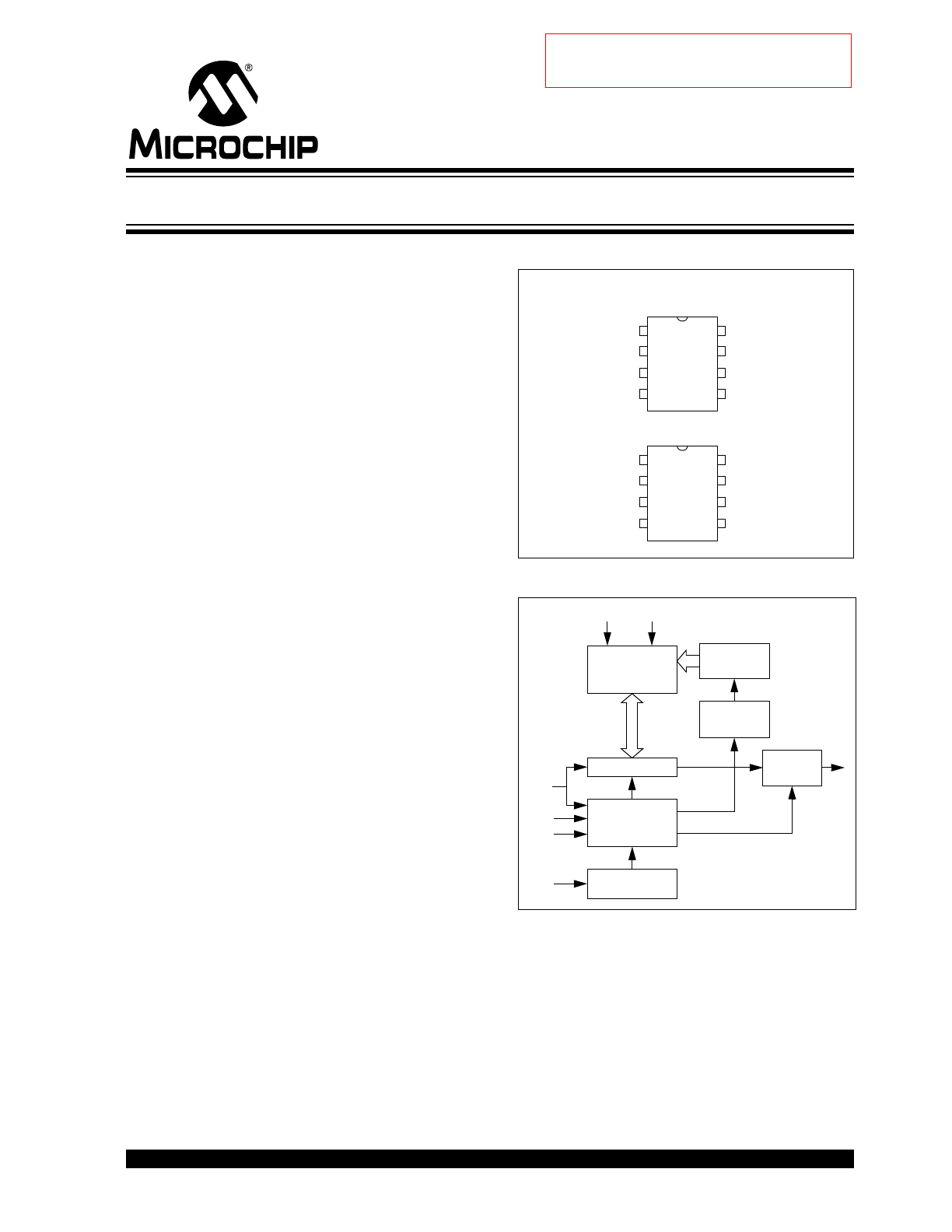
standard 8-pin PDIP and surface mount SOIC
packages. The rotated pin-out 93LC46X/56X/66X are
offered in the “SN” package only.
Package Types
Block Diagram
- Industrial (I):
-40°C to +85°C
93
LC
4
6
93
LC
5
6
93
LC
6
6
CS
CLK
DI
DO
1
2
3
4
8
7
6
5
V
CC
NU
ORG
V
SS
PDIP/SOIC
NU
V
CC
CS
CLK
1
2
3
4
8
7
6
5
ORG
V
SS
DO
DI
ROTATED SOIC
93
LC
4
6
X
93
LC
5
6
X
93
LC
6
6
X
Data Register
Output
Memory
Array
CLK
V
CC
V
SS
Clock
Mode
Decode
Logic
Register
CS
ORG
DI
Address
Decoder
Address
Counter
Buffer
DO
1K/2K/4K 2.5V Microwire Serial EEPROM
Not recommended for new designs –
Please use 93LC46C, 93LC56C or 93LC66C.
93LC46/56/66
DS21712C-page 2
2002-2012 Microchip Technology Inc.
1.0
ELECTRICAL CHARACTERISTICS
Absolute Maximum Ratings
(†)
V
CC
.............................................................................................................................................................................6.5V
All inputs and outputs w.r.t. V
SS
........................................................................................................ -0.6V to V
CC
+ 1.0V
Storage temperature ...............................................................................................................................-65°C to +150°C
Ambient temperature with power applied ................................................................................................-40°C to +125°C
ESD protection on all pins
4 kV
DC C
HARACTERISTICS
† NOTICE: Stresses above those listed under “Maximum ratings” may cause permanent damage to the device. This
is a stress rating only and functional operation of the device at those or any other conditions above those indicated in
the operational listings of this specification is not implied. Exposure to maximum rating conditions for extended periods
may affect device reliability.
DC CHARACTERISTICS
V
CC
= +2.5V to +5.5V
Industrial (I): T
A
= -40°C to +85°C
Param.
No.
Sym
Characteristic
Min
Typ
Max
Units
Conditions
D1
V
IH
1
High-level input voltage
2.0
—
V
CC
+1
V
V
CC
2.7V
V
IH
2
0.7 V
CC
—
V
CC
+1
V
V
CC
2.7V
D2
V
IL
1
Low-level input voltage
-0.3
—
0.8
V
V
CC
2.7V
V
IL
2
-0.3
—
0.2 V
CC
V
V
CC
2.7V
D3
V
OL
1
Low-level output voltage
—
—
0.4
V
I
OL
= 2.1 mA, V
CC
= 4.5V
V
OL
2
—
—
0.3
V
I
OL
= 100
A, V
CC
= 2.5V
D4
V
OH
1
High-level output voltage
2.4
—
—
V
I
OL
= 400
A, V
CC
= 4.5V
V
OH
2
V
CC
-0.2
—
—
V
I
OL
= 100
A, V
CC
= 2.5V
D5
I
LI
Input leakage current
—
—
±10
A
V
IN
= 0.1V to V
CC
D6
I
LO
Output leakage current
—
—
±10
A
V
OUT
= 0.1V to V
CC
D7
C
IN
,
C
OUT
Pin capacitance
(all inputs/outputs)
—
—
7
pF
V
IN
/V
OUT
= 0V (Note 1 & 2)
T
A
= 25°C, F
CLK
= 1 MHz
D8
I
CC
write
Operating current
—
—
3
mA
F
CLK
= 2 MHz, V
CC
= 5.5V
(Note 2)
D9
I
CC
read
—
—
—
—
—
100
1
500
—
mA
A
A
F
CLK
= 2 MHz, V
CC
= 5.5V
F
CLK
= 1 MHz, V
CC
= 3.0V
F
CLK
= 1 MHz, V
CC
= 2.5V
D10
I
CCS
Standby current
—
—
—
—
—
3
100
30
—
A
A
A
CLK = CS = 0V; V
CC
= 5.5V
CLK = CS = 0V; V
CC
= 3.0V
CLK = CS = 0V; V
CC
= 2.5V
ORG, DI = V
SS
or V
CC
Note 1:
This parameter is tested at T
A
= 25°C and F
CLK
= 1 MHz.
2:
This parameter is periodically sampled and not 100% tested.
2002-2012 Microchip Technology Inc.
DS21712C-page 3
93LC46/56/66
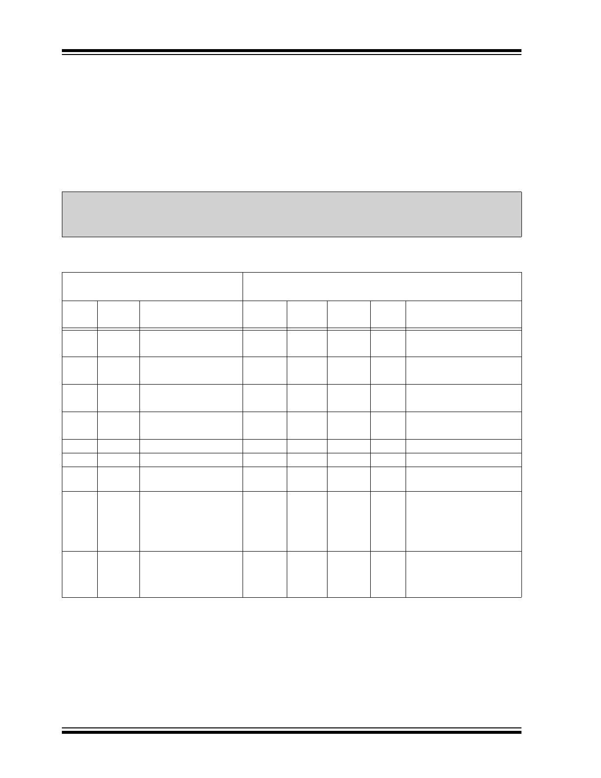
AC CHARACTERISTICS
FIGURE 1-1:
SYNCHRONOUS DATA TIMING
AC CHARACTERISTICS
V
CC
= +2.5V to +5.5V
Industrial (I): T
A
= -40°C to +85°C
Param.
No.
Sym
Characteristic
Min
Typ
Max
Units
Conditions
1
F
CLK
Clock frequency
—
—
—
—
2
1
MHz
MHz
V
CC
4.5V
V
CC
4.5V
2
T
CKH
Clock high time
250
—
—
ns
3
T
CKL
Clock low time
250
—
—
ns
4
T
CSS
Chip select setup time
50
—
—
ns
Relative to CLK
5
T
CSH
Chip select hold time
0
—
—
ns
Relative to CLK
6
T
CSL
Chip select low time
250
—
—
ns
7
T
DIS
Data input setup time
100
—
—
ns
Relative to CLK
8
T
DIH
Data input hold time
100
—
—
ns
Relative to CLK
9
T
PD
Data output delay time
—
—
400
ns
CL = 100 pF
10
T
CZ
Data output disable time
—
—
100
ns
CL = 100 pf (Note 2)
11
T
SV
Status valid time
—
—
500
ns
CL = 100 pF
12
T
WC
Program cycle time
—
4
10
ms
Erase/Write mode
13
T
EC
—
8
15
ms
ERAL mode (V
CC
=5V ±10%)
14
T
WL
—
16
30
ms
WRAL mode (V
CC
=5V ±10%)
15
—
Endurance
1M
—
1M
cycles
25°C, V
CC
= 5.0V, Block
mode (Note 3)
Note 1:
This parameter is tested at T
A
= 25°C and F
CLK
= 1 MHz.
2:
This parameter is periodically sampled and not 100% tested.
3:
This parameter is not tested but ensured by characterization. For endurance estimates in a specific
application, please consult the Total Endurance
™
Model which can be obtained from Microchip’s web site
at: www.microchip.com.
CS
V
IH
V
IL
V
IH
V
IL
V
IH
V
IL
V
OH
V
OL
V
OH
V
OL
CLK
DI
DO
(Read)
DO
(Write)
4
7
2
3
8
9
5
9
10
Status Valid
11
10
93LC46/56/66
DS21712C-page 4
2002-2012 Microchip Technology Inc.
TABLE 1-1:
INSTRUCTION SET FOR 93LC46: ORG = 1 (X 16 ORGANIZATION)
TABLE 1-2:
INSTRUCTION SET FOR 93LC46: ORG = 0 (X 8 ORGANIZATION)
TABLE 1-3:
INSTRUCTION SET FOR 93LC56: ORG = 1 (X 16 ORGANIZATION)
TABLE 1-4:
INSTRUCTION SET FOR 93LC56: ORG = 0 (X 8 ORGANIZATION)
Instruction
SB
Opcode
Address
Data In
Data Out
Req. CLK
Cycles
READ
1
10
A5 A4 A3 A2 A1 A0
—
D15 - D0
25
EWEN
1
00
1 1 XXXX
—
High-Z
9
ERASE
1
11
A5 A4 A3 A2 A1 A0
—
(RDY/BSY)
9
ERAL
1
00
1 0 XXXX
—
(RDY/BSY)
9
WRITE
1
01
A5 A4 A3 A2 A1 A0
D15 - D0
(RDY/BSY)
25
WRAL
1
00
0 1 XXXX
D15 - D0
(RDY/BSY)
25
EWDS
1
00
0 0 XXXX
—
High-Z
9
Instruction
SB
Opcode
Address
Data In
Data Out
Req. CLK
Cycles
READ
1
10
A6 A5 A4 A3 A2 A1 A0
—
D7 - D0
18
EWEN
1
00
1 1 X X X X X
—
High-Z
10
ERASE
1
11
A6 A5 A4 A3 A2 A1 A0
—
(RDY/BSY)
10
ERAL
1
00
1 0 X X X X X
—
(RDY/BSY)
10
WRITE
1
01
A6 A5 A4 A3 A2 A1 A0
D7 - D0
(RDY/BSY)
18
WRAL
1
00
0 1 X X X X X
D7 - D0
(RDY/BSY)
18
EWDS
1
00
0 0 X X X X X
—
High-Z
10
Instruction
SB
Opcode
Address
Data In
Data Out
Req. CLK
Cycles
READ
1
10
X A6 A5 A4 A3 A2 A1 A0
—
D15 - D0
27
EWEN
1
00
1 1 X X X X X X
—
High-Z
11
ERASE
1
11
X A6 A5 A4 A3 A2 A1 A0
—
(RDY/BSY)
11
ERAL
1
00
1 0 X X X X X X
—
(RDY/BSY)
11
WRITE
1
01
X A6 A5 A4 A3 A2 A1 A0
D15 - D0
(RDY/BSY)
27
WRAL
1
00
0 1 X X X X X X
D15 - D0
(RDY/BSY)
27
EWDS
1
00
0 0 X X X X X X
—
High-Z
11
Instruction
SB
Opcode
Address
Data In
Data Out
Req. CLK
Cycles
READ
1
10
X A7 A6 A5 A4 A3 A2 A1 A0
—
D7 - D0
20
EWEN
1
00
1 1 X X X X X X X
—
High-Z
12
ERASE
1
11
X A7 A6 A5 A4 A3 A2 A1 A0
—
(RDY/BSY)
12
ERAL
1
00
1 0 X X X X X X X
—
(RDY/BSY)
12
WRITE
1
01
X A7 A6 A5 A4 A3 A2 A1 A0
D7 - D0
(RDY/BSY)
20
WRAL
1
00
0 1 X X X X X X X
D7 - D0
(RDY/BSY)
20
EWDS
1
00
0 0 X X X X X X X
—
High-Z
12
2002-2012 Microchip Technology Inc.
DS21712C-page 5
93LC46/56/66
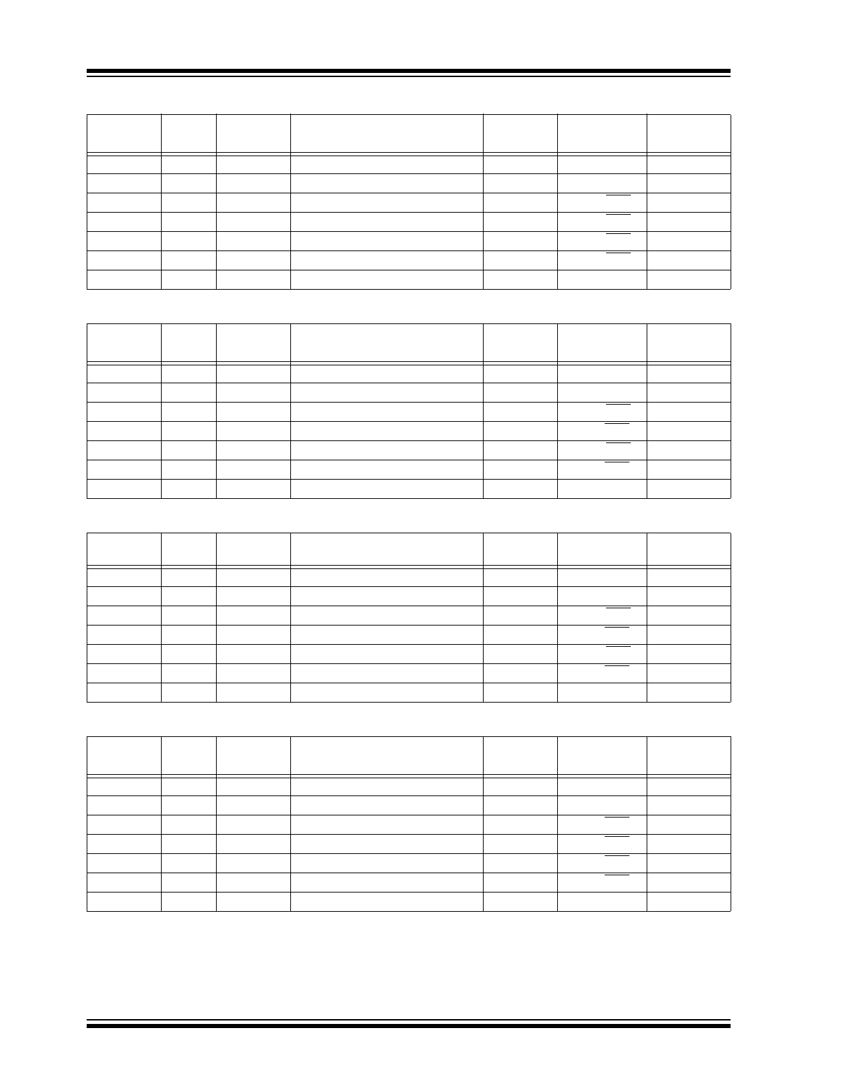
TABLE 1-5:
INSTRUCTION SET FOR 93LC66: ORG = 1 (X 16 ORGANIZATION)
TABLE 1-6:
INSTRUCTION SET FOR 93LC66: ORG = 0 (X 8 ORGANIZATION)
Instruction
SB
Opcode
Address
Data In
Data Out
Req. CLK
Cycles
READ
1
10
A7 A6 A5 A4 A3 A2 A1 A0
—
D15 - D0
27
EWEN
1
00
1 1 X X X X X X
—
High-Z
11
ERASE
1
11
A7 A6 A5 A4 A3 A2 A1 A0
—
(RDY/BSY)
11
ERAL
1
00
1 0 X X X X X X
—
(RDY/BSY)
11
WRITE
1
01
A7 A6 A5 A4 A3 A2 A1 A0
D15 - D0
(RDY/BSY)
27
WRAL
1
00
0 1 X X X X X X
D15 - D0
(RDY/BSY)
27
EWDS
1
00
0 0 X X X X X X
—
High-Z
11
Instruction
SB
Opcode
Address
Data In
Data Out
Req. CLK
Cycles
READ
1
10
A8 A7 A6 A5 A4 A3 A2 A1 A0
—
D7 - D0
20
EWEN
1
00
1 1 X X X X X X X
—
High-Z
12
ERASE
1
11
A8 A7 A6 A5 A4 A3 A2 A1 A0
—
(RDY/BSY)
12
ERAL
1
00
1 0 X X X X X X X
—
(RDY/BSY)
12
WRITE
1
01
A8 A7 A6 A5 A4 A3 A2 A1 A0
D7 - D0
(RDY/BSY)
20
WRAL
1
00
0 1 X X X X X X X
D7 - D0
(RDY/BSY)
20
EWDS
1
00
0 0 X X X X X X X
—
High-Z
12

93LC46/56/66
DS21712C-page 6
2002-2012 Microchip Technology Inc.
2.0
FUNCTIONAL DESCRIPTION
When the ORG pin is connected to V
CC
, the (x16)
organization is selected. When it is connected to
ground, the (x8) organization is selected. Instruc-
tions, addresses and write data are clocked into the
DI pin on the rising edge of the clock (CLK). The DO
pin is normally held in a high-Z state except when
reading data from the device, or when checking the
Ready/Busy status during a programming operation.
The Ready/Busy status can be verified during an
erase/write operation by polling the DO pin; DO low
indicates that programming is still in progress, while
DO high indicates the device is ready. The DO will
enter the high-Z state on the falling edge of the CS.
2.1
Start Condition
The Start bit is detected by the device if CS and DI are
both high with respect to the positive edge of CLK for
the first time.
Before a Start condition is detected, CS, CLK and DI
may change in any combination (except to that of a
Start condition), without resulting in any device opera-
tion (Read, Write, Erase, EWEN, EWDS, ERAL and
WRAL). As soon as CS is high, the device is no longer
in the Standby mode.
An instruction following a Start condition will only be
executed if the required amount of opcode, address
and data bits for any particular instruction is clocked in.
After execution of an instruction (i.e., clock in or out of
the last required address or data bit) CLK and DI
become “don't care” bits until a new Start condition is
detected.
2.2
Data In/Data Out (DI/DO)
It is possible to connect the Data In and Data Out pins
together. However, with this configuration it is possible
for a “bus conflict” to occur during the “dummy zero”
that precedes the read operation, if A0 is a logic high
level. Under such a condition the voltage level seen at
Data Out is undefined and will depend upon the relative
impedances of Data Out and the signal source driving
A0. The higher the current sourcing capability of A0,
the higher the voltage at the Data Out pin.
2.3
Data Protection
During power-up, all programming modes of operation
are inhibited until V
CC
has reached a level greater than
1.4V. During power-down, the source data protection
circuitry acts to inhibit all programming modes when
V
CC
has fallen below 1.4V at nominal conditions.
The EWEN and EWDS commands give additional
protection against accidentally programming during
normal operation.
After power-up, the device is automatically in the
EWDS mode. Therefore, an EWEN instruction must be
performed before any ERASE or WRITE instruction can
be executed.
2.4
Read
The READ instruction outputs the serial data of the
addressed memory location on the DO pin. A dummy
zero bit precedes the 16-bit (x16 organization) or 8-bit
(x8 organization) output string. The output data bits will
toggle on the rising edge of the CLK and are stable
after the specified time delay (T
PD
). Sequential read is
possible when CS is held high. The memory data will
automatically cycle to the next register and output
sequentially.
2.5
Erase/Write Enable and Disable
(EWEN, EWDS)
The 93LC46/56/66 power up in the Erase/Write Disable
(EWDS) state. All programming modes must be
preceded by an Erase/Write Enable (EWEN) instruction.
Once the EWEN instruction is executed, programming
remains enabled until an EWDS instruction is executed
or V
CC
is removed from the device. To protect against
accidental data disturb, the EWDS instruction can be
used to disable all erase/write functions and should
follow all programming operations. Execution of a READ
instruction is independent of both the EWEN and EWDS
instructions.
2.6
Erase
The ERASE instruction forces all data bits of the speci-
fied address to the logical “1” state. CS is brought low
following the loading of the last address bit. This falling
edge of the CS pin initiates the self-timed programming
cycle.
The DO pin indicates the Ready/Busy status of the
device if CS is brought high after a minimum of 250 ns
low (T
CSL
). DO at logical “0” indicates that program-
ming is still in progress. DO at logical “1” indicates that
the register at the specified address has been erased
and the device is ready for another instruction.
The erase cycle takes 4 ms per word typical.
2002-2012 Microchip Technology Inc.
DS21712C-page 7
93LC46/56/66
2.7
Write
The WRITE instruction is followed by 16 bits (or by 8
bits) of data which are written into the specified
address. After the last data bit is put on the DI pin,
CS must be brought low before the next rising edge
of the CLK clock. This falling edge of CS initiates the
self-timed auto-erase and programming cycle.
The DO pin indicates the Ready/Busy status of the
device if CS is brought high after a minimum of 250 ns
low (T
CSL
) and before the entire write cycle is complete.
DO at logical “0” indicates that programming is still in
progress. DO at logical “1” indicates that the register at
the specified address has been written with the data
specified and the device is ready for another
instruction.
The write cycle takes 4 ms per word typical.
2.8
Erase All (ERAL)
The ERAL instruction will erase the entire memory array
to the logical “1” state. The ERAL cycle is identical to
the ERASE cycle except for the different opcode. The
ERAL cycle is completely self-timed and commences
at the falling edge of the CS. Clocking of the CLK pin is
not necessary after the device has entered the self
clocking mode. The ERAL instruction is ensured at 5V
±10%.
The DO pin indicates the Ready/Busy status of the
device if CS is brought high after a minimum of 250 ns
low (T
CSL
) and before the entire write cycle is complete.
The ERAL cycle takes (8 ms typical).
2.9
Write All (WRAL)
The WRAL instruction will write the entire memory array
with the data specified in the command. The WRAL
cycle is completely self-timed and commences at the
falling edge of the CS. Clocking of the CLK pin is not
necessary after the device has entered the self clock-
ing mode. The WRAL command does include an auto-
matic ERAL cycle for the device. Therefore, the WRAL
instruction does not require an ERAL instruction but the
chip must be in the EWEN status. The WRAL instruction
is ensured at 5V ±10%.
The DO pin indicates the Ready/Busy status of the
device if CS is brought high after a minimum of 250 ns
low (Tcsl).
The WRAL cycle takes 16 ms typical.
FIGURE 2-1:
READ TIMING
CS
CLK
DI
DO
1
1
0
An
•••
A0
High-Z
0
Dx
•••
D0
Dx
•••
D0
•••
Dx
D0
93LC46/56/66
DS21712C-page 8
2002-2012 Microchip Technology Inc.
FIGURE 2-2:
EWEN TIMING
FIGURE 2-3:
EWDS TIMING
FIGURE 2-4:
WRITE TIMING
1
X
CS
DI
0
0
1
1
X
6
•••
CS
CLK
DI
1
0
0
0
0
X
•••
X
6
CS
CLK
DI
DO
1
0
1
An
•••
A0
Dx
•••
D0
Busy
Ready
High-Z
12
6
11
2002-2012 Microchip Technology Inc.
DS21712C-page 9
93LC46/56/66
FIGURE 2-5:
WRAL TIMING
FIGURE 2-6:
ERASE TIMING
FIGURE 2-7:
ERAL TIMING
CS
CLK
DI
DO
High-Z
1
0
0
0
1
X
•••
X
Dx
•••
D0
High-Z
Busy
Ready
14
Ensured by Characterization at V
CC
= 4.5V to +5.5V
.
6
11
10
CS
CLK
DI
DO
6
Check Status
1
1
1
An
An-1
An-2
•••
A0
11
10
Busy
Ready
High-Z
12
High-Z
CS
CLK
DI
DO
6
Check Status
1
0
0
1
0
X
•••
X
11
10
Busy
Ready
High-Z
13
High-Z
Ensured by Characterization at Vcc = 4.5V to +5.5V.
93LC46/56/66
DS21712C-page 10
2002-2012 Microchip Technology Inc.
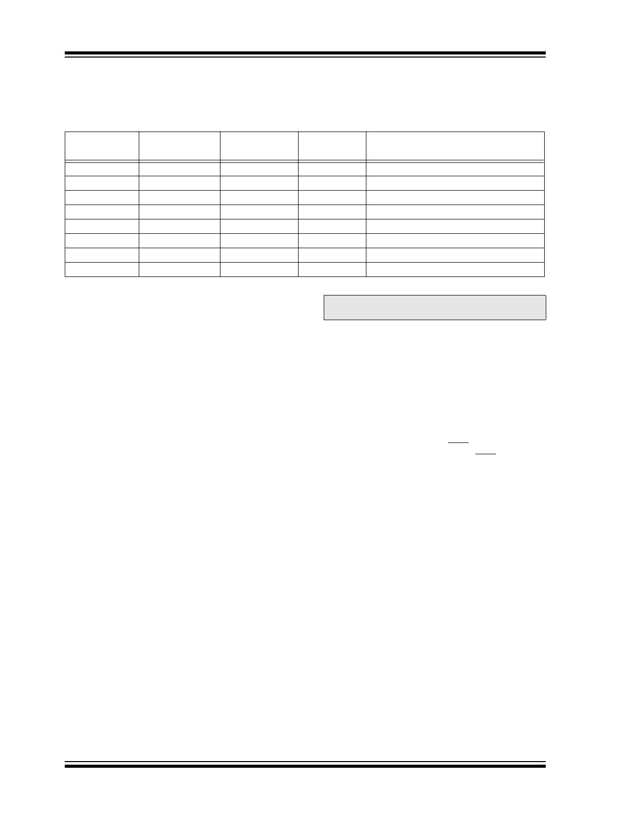
3.0
PIN DESCRIPTION
The descriptions of the pins are listed in Table 3-1.
TABLE 3-1:
PIN FUNCTION TABLE
3.1
Chip Select (CS)
A high level selects the device. A low level deselects
the device and forces it into Standby mode. However, a
programming cycle which is already initiated and/or in
progress will be completed, regardless of the CS input
signal. If CS is brought low during a program cycle, the
device will go into Standby mode as soon as the
programming cycle is completed.
CS must be low for 250 ns minimum (T
CSL
) between
consecutive instructions. If CS is low, the internal
control logic is held in a Reset status.
3.2
Serial Clock (CLK)
The serial clock is used to synchronize the communica-
tion between a master device and the 93LC46/56/66.
Opcode, address and data bits are clocked in on the
positive edge of CLK. Data bits are also clocked out on
the positive edge of CLK.
CLK can be stopped anywhere in the transmission
sequence (at high or low level) and can be continued
anytime with respect to clock high time (T
CKH
) and
clock low time (T
CKL
). This gives the controlling master
freedom in preparing opcode, address and data.
CLK is a “don't care” if CS is low (device deselected). If
CS is high, but Start condition has not been detected,
any number of clock cycles can be received by the
device without changing its status (i.e., waiting for Start
condition).
CLK cycles are not required during the self-timed write
(i.e., auto erase/write) cycle.
After detection of a Start condition the specified number
of clock cycles (respectively low-to-high transitions of
CLK) must be provided. These clock cycles are required
to clock in all required opcode, address and data bits
before an instruction is executed (see instruction set
truth table). CLK and DI then become “don't care” inputs
waiting for a new Start condition to be detected.
3.3
Data In (DI)
Data In is used to clock in a Start bit, opcode, address
and data synchronously with the CLK input.
3.4
Data Out (DO)
Data Out is used in the Read mode to output data syn-
chronously with the CLK input (T
PD
after the positive
edge of CLK).
This pin also provides Ready/Busy status information
during erase and write cycles. Ready/Busy status infor-
mation is available on the DO pin if CS is brought high
after being low for minimum chip select low time (T
CSL
)
and an erase or write operation has been initiated.
The Status signal is not available on DO, if CS is held
low or high during the entire write or erase cycle. In all
other cases DO is in the High-Z mode. If status is
checked after the write/erase cycle, a pull-up resistor
on DO is required to read the Ready signal.
3.5
Organization (ORG)
When ORG is connected to V
CC
, the (x16) memory
organization is selected. When ORG is tied to V
SS
, the
(x8) memory organization is selected. ORG can only be
floated for clock speeds of 1 MHz or less for the (x16)
memory organization. For clock speeds greater than
1 MHz, ORG must be tied to V
CC
or V
SS
.
Name
PDIP
SOIC
ROTATED
TSSOP
Description
CS
1
1
3
Chip Select
CLK
2
2
4
Serial Data Clock
DI
3
3
5
Serial Data Input
DO
4
4
6
Serial Data Output
V
SS
5
5
7
Ground
ORG
6
6
8
Memory Configuration
NU
7
7
1
Not Utilized
Vcc
8
8
2
+1.8V to 5.5V Power Supply
Note:
CS must go low between consecutive
instructions.