
2002-2013 Microchip Technology Inc.
DS21705B-page 1
MCP73826
Features
• Linear Charge Management Controller for Single
Lithium-Ion Cells
• High Accuracy Preset Voltage Regulation:
+1% (max)
• Two Preset Voltage Regulation Options:
- 4.1V - MCP73826-4.1
- 4.2V - MCP73826-4.2
• Programmable Charge Current
• Automatic Cell Preconditioning of Deeply
Depleted Cells, Minimizing Heat Dissipation Dur-
ing Initial Charge Cycle
• Automatic Power-Down when Input Power
Removed
• Temperature Range: -20°C to +85°C
• Packaging: 6-Pin SOT-23A
Applications
• Single Cell Lithium-Ion Battery Chargers
• Personal Data Assistants
• Cellular Telephones
• Hand Held Instruments
• Cradle Chargers
• Digital Cameras
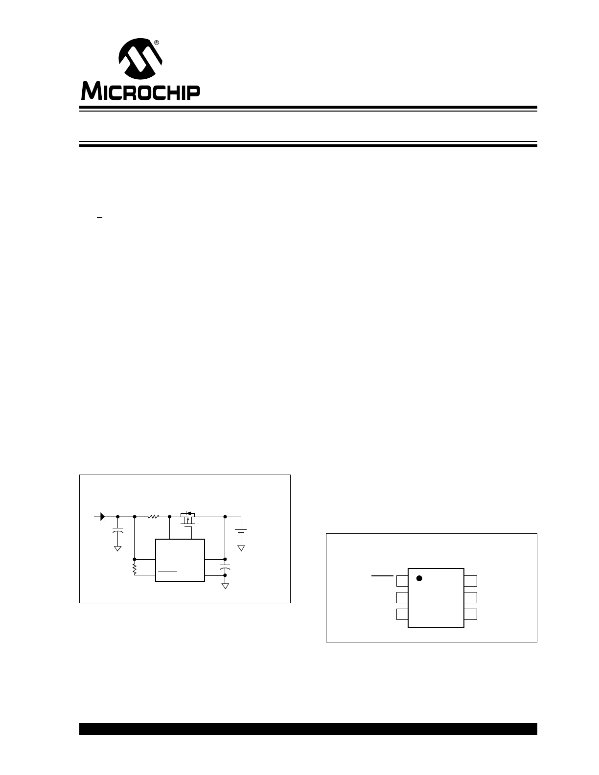
Typical Application Circuit
Description
The MCP73826 is a linear charge management con-
troller for use in space-limited, cost sensitive applica-
tions. The MCP73826 combines high accuracy
constant voltage, controlled current regulation, and cell
preconditioning in a space saving 6-pin SOT-23A pack-
age. The MCP73826 provides a stand-alone charge
management solution.
The MCP73826 charges the battery in three phases:
preconditioning, controlled current, and constant volt-
age. If the battery voltage is below the internal low-volt-
age threshold, the battery is preconditioned with a
foldback current. The preconditioning phase protects
the lithium-ion cell and minimizes heat dissipation.
Following the preconditioning phase, the MCP73826
enters the controlled current phase. The MCP73826
allows for design flexibility with a programmable charge
current set by an external sense resistor. The charge
current is ramped up, based on the cell voltage, from
the foldback current to the peak charge current estab-
lished by the sense resistor. This phase is maintained
until the battery reaches the charge-regulation voltage.
Then, the MCP73826 enters the final phase, constant
voltage. The accuracy of the voltage regulation is better
than ±1% over the entire operating temperature range
and supply voltage range. The MCP73826-4.1 is preset
to a regulation voltage of 4.1V, while the MCP73826-
4.2 is preset to 4.2V.
The MCP73826 operates with an input voltage range
from 4.5V to 5.5V. The MCP73826 is fully specified
over the ambient temperature range of -20°C to +85°C.
Package Type
+
-
GND
V
DRV
V
SNS
V
IN
V
BAT
SHDN
1
2
3
6
5
4
10 µF
100 k
100 m
V
IN
Single
Lithium-Ion
Cell
NDS8434
MA2Q705
500 mA Lithium-Ion Battery Charger
5V
10 µF
MCP73826
6-Pin SOT-23A
GND
V
DRV
V
SNS
V
IN
V
BAT
SHDN 1
2
3
6
5
MCP73826
4
Single Cell Lithium-Ion Charge Management Controller
MCP73826
DS21705B-page 2
2002-2013 Microchip Technology Inc.
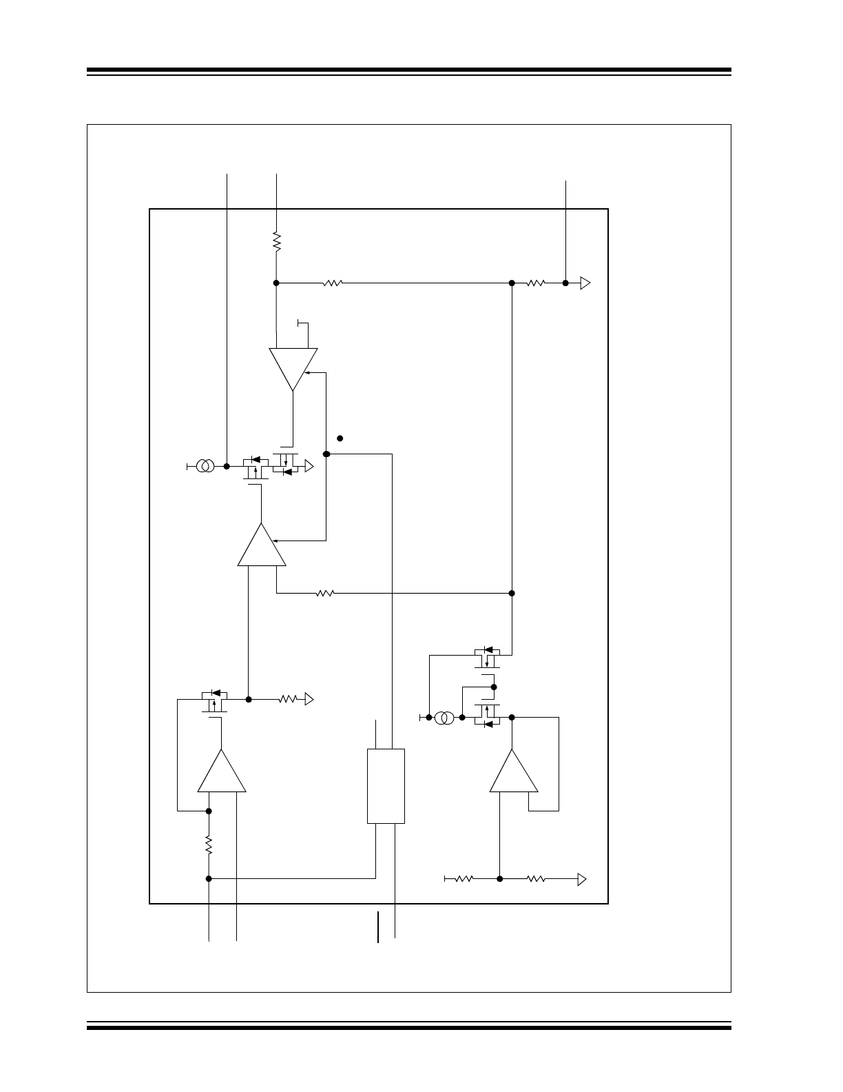
Functional Block Diagram
VO
L
T
AGE
C
O
N
T
R
O
L
AM
PLI
F
IE
R
S
HUT
DOW
N
,
RE
F
E
RE
NCE
GE
NE
RA
T
O
R
V
RE
F
(1.
2
V)
+
–
V
RE
F
V
IN
CHA
RGE
CURR
E
N
T
CONT
ROL A
M
P
L
IF
IE
R
+
–
V
RE
F
S
HDN
V
BA
T
GND
V
DRV
+
–
CHA
R
G
E
CURRE
NT
AM
PLI
F
IE
R
V
IN
V
SN
S
1.
1
k
12
k
500
k
75
k
75
k
352.
5
k
(NO
T
E
1)
CHA
RGE
CURRE
N
T
FOL
D
BA
C
K
AM
PL
IF
IE
R
+
–
37.
5
k
1
12.
5
k
V
IN
0.
3V CLA
M
P
N
OTE
1
:
V
a
lue =
340.
5K
f
o
r M
C
P738
26-4.
1
V
a
lue =
352.
5K
f
o
r MCP
73826-4.
2
2002-2013 Microchip Technology Inc.
DS21705B-page 3
MCP73826
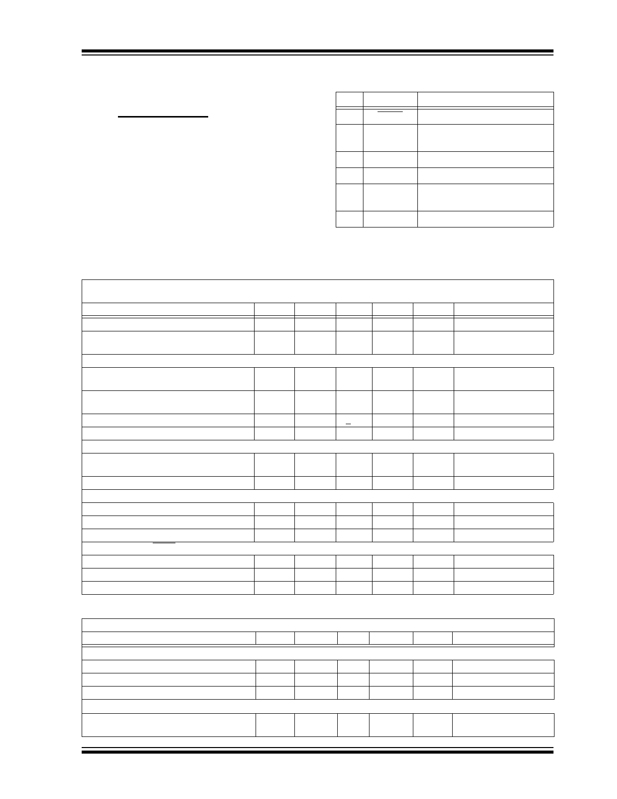
1.0
ELECTRICAL
CHARACTERISTICS
1.1
Maximum Ratings*
V
IN
................................................................................... -0.3V to 6.0V
All inputs and outputs w.r.t. GND ................-0.3 to (V
IN
+0.3)V
Current at V
DRV
.......................................................... +/-1 mA
Maximum Junction Temperature, T
J
.............................. 150°C
Storage temperature .....................................-65°C to +150°C
ESD protection on all pins
4 kV
*Notice: Stresses above those listed under “Maximum Ratings” may
cause permanent damage to the device. This is a stress rating only and
functional operation of the device at those or any other conditions
above those indicated in the operational listings of this specification is
not implied. Exposure to maximum rating conditions for extended peri-
ods may affect device reliability.
PIN FUNCTION TABLE
DC CHARACTERISTICS: MCP73826-4.1, MCP73826-4.2
TEMPERATURE SPECIFICATIONS
Pin
Name
Description
1
SHDN
Logic Shutdown
2
GND
Battery Management
0V Reference
3
V
BAT
Cell Voltage Monitor Input
4
V
DRV
Drive Output
5
V
IN
Battery Management
Input Supply
6
V
SNS
Charge Current Sense Input
Unless otherwise specified, all limits apply for V
IN
= [V
REG
(typ)+1V], R
SENSE
= 500 m
T
A
= -20°C to +85°C.
Typical values are at +25°C. Refer to Figure 1-1 for test circuit.
Parameter
Sym
Min
Typ
Max
Units
Conditions
Supply Voltage
V
IN
4.5
—
5.5
V
Supply Current
I
IN
—
—
0.5
260
15
560
µA
Shutdown, V
SHDN
= 0V
Constant Voltage Mode
Voltage Regulation (Constant Voltage Mode)
Regulated Output Voltage
V
REG
4.059
4.158
4.1
4.2
4.141
4.242
V
V
MCP73826-4.1 only
MCP73826-4.2 only
Line Regulation
V
BAT
-10
—
10
mV
V
IN
= 4.5V to 5.5V,
I
OUT
= 75 mA
Load Regulation
V
BAT
-1
+0.2
1
mV
I
OUT
= 10 mA to 75 mA
Output Reverse Leakage Current
I
LK
—
8
—
µA
V
IN
=Floating, V
BAT
=V
REG
External MOSFET Gate Drive
Gate Drive Current
I
DRV
—
0.08
—
—
1
—
mA
mA
Sink, CV Mode
Source, CV Mode
Gate Drive Minimum Voltage
V
DRV
—
1.6
—
V
Current Regulation (Controlled Current Mode)
Current Sense Gain
A
CS
—
100
—
dB
(V
SNS
-V
DRV
) /
V
BAT
Current Limit Threshold
V
CS
40
53
75
mV
(V
IN
-V
SNS
) at I
OUT
Foldback Current Scale Factor
K
—
0.43
—
A/A
Shutdown Input - SHDN
Input High Voltage Level
V
IH
40
—
—
%V
IN
Input Low Voltage Level
V
IL
—
—
25
%V
IN
Input Leakage Current
I
LK
—
—
1
µA
V
SHDN
= 0V to 5.5V
Unless otherwise specified, all limits apply for V
IN
= 4.5V-5.5V
Parameters
Sym
Min
Typ
Max
Units
Conditions
Temperature Ranges
Specified Temperature Range
T
A
-20
—
+85
°C
Operating Temperature Range
T
A
-40
—
+125
°C
Storage Temperature Range
T
A
-65
—
+150
°C
Thermal Package Resistances
Thermal Resistance, 6-Pin SOT-23A
JA
—
230
—
°C/W
4-Layer JC51-7 Standard
Board, Natural Convection
MCP73826
DS21705B-page 4
2002-2013 Microchip Technology Inc.
FIGURE 1-1:
MCP73826 Test Circuit.
GND
V
DRV
V
SNS
V
IN
V
BAT
SHDN
1
2
3
6
5
4
22 µF
22 µF
100 k
R
SENSE
V
IN
= 5.1V
NDS8434
I
OUT
V
OUT
(MCP73826-4.1)
V
IN
= 5.2V
(MCP73826-4.2)
MCP73826
2002-2013 Microchip Technology Inc.
DS21705B-page 5
MCP73826
2.0
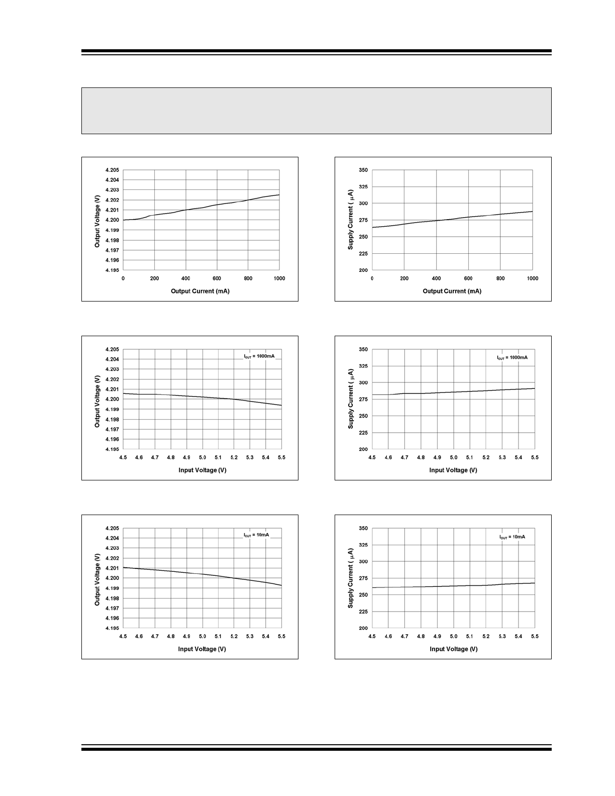
TYPICAL PERFORMANCE CHARACTERISTICS
Note: Unless otherwise indicated, I
OUT
= 10 mA, Constant Voltage Mode, T
A
= 25°C. Refer to Figure 1-1 for test circuit.
FIGURE 2-1:
Output Voltage vs. Output Current
(MCP73826-4.2).
FIGURE 2-2:
Output Voltage vs. Input Voltage
(MCP73826-4.2).
FIGURE 2-3:
Output Voltage vs. Input Voltage
(MCP73826-4.2).
FIGURE 2-4:
Supply Current vs. Output Current.
FIGURE 2-5:
Supply Current vs. Input Voltage.
FIGURE 2-6:
Supply Current vs. Input Voltage.
Note:
The graphs and tables provided following this note are a statistical summary based on a limited number of
samples and are provided for informational purposes only. The performance characteristics listed herein
are not tested or guaranteed. In some graphs or tables, the data presented may be outside the specified
operating range (e.g., outside specified power supply range) and therefore outside the warranted range.
MCP73826
DS21705B-page 6
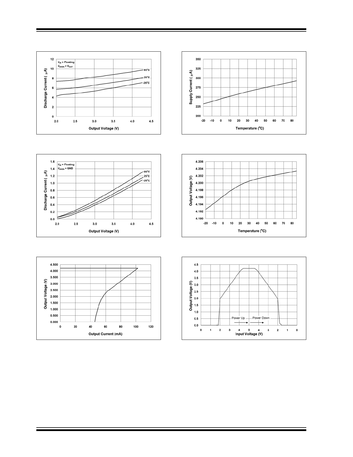
2002-2013 Microchip Technology Inc.
Note: Unless otherwise indicated, I
OUT
= 10 mA, Constant Voltage Mode, T
A
= 25°C. Refer to Figure 1-1 for test circuit.
FIGURE 2-7:
Output Reverse Leakage Current vs.
Output Voltage.
FIGURE 2-8:
Output Reverse Leakage Current vs.
Output Voltage.
FIGURE 2-9:
Current Limit Foldback.
FIGURE 2-10: Supply Current vs. Temperature.
FIGURE 2-11: Output Voltage vs. Temperature
(MCP73826-4.2).
FIGURE 2-12: Power-Up / Power-Down.
2002-2013 Microchip Technology Inc.
DS21705B-page 7
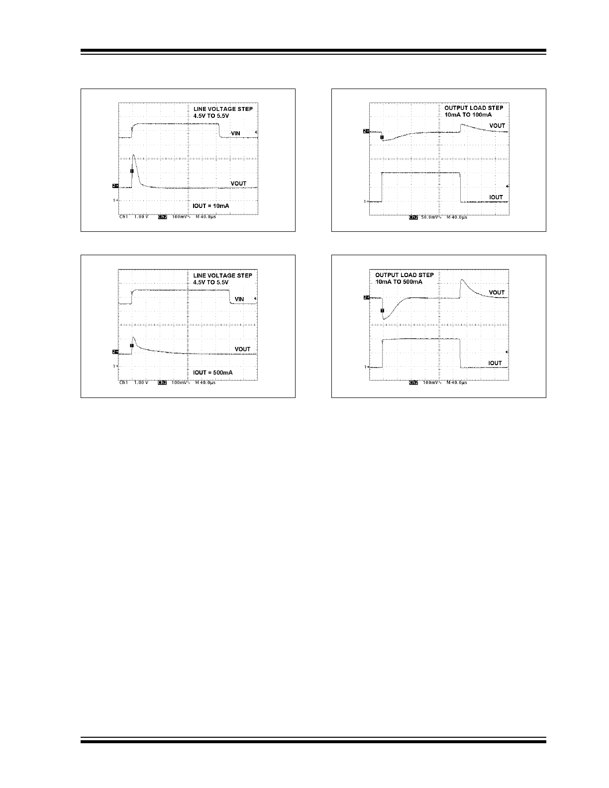
MCP73826
Note: Unless otherwise indicated, I
OUT
= 10 mA, Constant Voltage Mode, T
A
= 25°C. Refer to Figure 1-1 for test circuit.
FIGURE 2-13: Line Transient Response.
FIGURE 2-14: Line Transient Response.
FIGURE 2-15: Load Transient Response.
FIGURE 2-16: Load Transient Response.
MCP73826
DS21705B-page 8
2002-2013 Microchip Technology Inc.
3.0
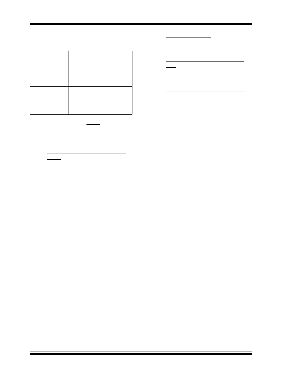
PIN DESCRIPTION
The descriptions of the pins are listed in Table 3-1.
TABLE 3-1:
Pin Function Table.
3.1
Logic Shutdown (SHDN)
Input to force charge termination, initiate charge, or ini-
tiate recharge.
3.2
Battery Management 0V Reference
(GND)
Connect to negative terminal of battery.
3.3
Cell Voltage Monitor Input (V
BAT
)
Voltage sense input. Connect to positive terminal of
battery. Bypass to GND with a minimum of 10 µF to
ensure loop stability when the battery is disconnected.
A precision internal resistor divider regulates the final
voltage on this pin to V
REG
.
3.4
Drive Output (V
DRV
)
Direct output drive of an external P-channel MOSFET
pass transistor for current and voltage regulation.
3.5
Battery Management Input Supply
(V
IN
)
A supply voltage of 4.5V to 5.5V is recommended.
Bypass to GND with a minimum of 10 µF.
3.6
Charge Current Sense Input (V
SNS
)
Charge current is sensed via the voltage developed
across an external precision sense resistor. The sense
resistor must be placed between the supply voltage
(V
IN
) and the source of the external pass transistor. A
50 m
sense resistor produces a fast charge current of
1 A, typically.
Pin
Name
Description
1
SHDN
Logic Shutdown
2
GND
Battery Management
0V Reference
3
V
BAT
Cell Voltage Monitor Input
4
V
DRV
Drive Output
5
V
IN
Battery Management
Input Supply
6
V
SNS
Charge Current Sense Input
2002-2013 Microchip Technology Inc.
DS21705B-page 9
MCP73826
4.0
DEVICE OVERVIEW
The MCP73826 is a linear charge management con-
troller. Refer to the functional block diagram on page 2
and the typical application circuit, Figure 6-1.
4.1
Charge Qualification and
Preconditioning
Upon insertion of a battery or application of an external
supply, the MCP73826 verifies the state of the SHDN
pin. The SHDN pin must be above the logic high level.
If the SHDN pin is above the logic high level, the
MCP73826 initiates a charge cycle. If the cell is below
the preconditioning threshold, 2.4V typically, the
MCP73826 preconditions the cell with a scaled back
current. The preconditioning current is set to approxi-
mately 43% of the fast charge peak current. The pre-
conditioning safely replenishes deeply depleted cells
and minimizes heat dissipation in the external pass
transistor during the initial charge cycle.
4.2
Controlled Current Regulation - Fast
Charge
Preconditioning ends and fast charging begins when
the cell voltage exceeds the preconditioning threshold.
Fast charge utilizes a foldback current scheme based
on the voltage at the V
SNS
input developed by the drop
across an external sense resistor, R
SENSE
, and the out-
put voltage,
V
BAT
. Fast charge continues until the cell
voltage reaches the regulation voltage, V
REG
.
4.3
Constant Voltage Regulation
When the cell voltage reaches the regulation voltage,
V
REG
, constant voltage regulation begins. The
MCP73826 monitors the cell voltage at the
V
BAT
pin.
This input is tied directly to the positive terminal of the
battery. The MCP73826 is offered in two fixed-voltage
versions for battery packs with either coke or graphite
anodes: 4.1V (MCP73826-4.1) and 4.2V
(MCP73826-4.2).
4.4
Charge Cycle Completion
The charge cycle can be terminated by a host micro-
controller after an elapsed time from the start of the
charge cycle. The charge is terminated by pulling the
shutdown pin, SHDN, to a logic Low level.

MCP73826
DS21705B-page 10
2002-2013 Microchip Technology Inc.
5.0
DETAILED DESCRIPTION
Refer to the typical application circuit, Figure 6-1.
5.1
Analog Circuitry
5.1.1
OUTPUT VOLTAGE INPUT (
V
BAT
)
The MCP73826 monitors the cell voltage at the
V
BAT
pin. This input is tied directly to the positive terminal of
the battery. The MCP73826 is offered in two fixed-volt-
age versions for single cells with either coke or graphite
anodes: 4.1V (MCP73826-4.1) and 4.2V
(MCP73826-4.2).
5.1.2
GATE DRIVE OUTPUT (V
DRV
)
The MCP73826 controls the gate drive to an external
P-channel MOSFET, Q1. The P-channel MOSFET is
controlled in the linear region, regulating current and
voltage supplied to the cell. The drive output is auto-
matically turned off when the input supply falls below
the voltage sensed on the
V
BAT
input.
5.1.3
SUPPLY VOLTAGE (V
IN
)
The V
IN
input is the input supply to the MCP73826. The
MCP73826 automatically enters a power-down mode if
the voltage on the V
IN
input falls below the voltage on
the
V
BAT
pin. This feature prevents draining the battery
pack when the V
IN
supply is not present.
5.1.4
CURRENT SENSE INPUT (V
SNS
)
Fast charge current regulation is maintained by the
voltage drop developed across an external sense resis-
tor, R
SENSE
, applied to the V
SNS
input pin. The follow-
ing formula calculates the value for R
SENSE
:
Where:
V
CS
is the current limit threshold
I
OUT
is the desired peak fast charge current in
amps. The preconditioning current is scaled to
approximately 43% of I
OUT
.
5.2
Digital Circuitry
5.2.1
SHUTDOWN INPUT (SHDN)
The shutdown input pin, SHDN, can be used to termi-
nate a charge anytime during the charge cycle, initiate
a charge cycle, or initiate a recharge cycle.
Applying a logic High input signal to the SHDN pin, or
tying it to the input source, enables the device. Apply-
ing a logic Low input signal disables the device and ter-
minates a charge cycle. In shutdown mode, the
device’s supply current is reduced to 0.5 µA, typically.
R
SENSE
V
CS
I
OUT
------------
=