
2001-2012 Microchip Technology Inc.
DS21688D-page 1
TC670
Features
• Fan Wear-Out Detection for 2-Wire
Linear-Controlled Fans
• Replacement System for 3-Wire Fans
• Fan Alert Signal when Fan Speed is below
Programmed Threshold
• CLEAR Capability for Eliminating False Alarm
• Low Operating Current, 90 µA (typ.)
• V
DD
Range 3.0V to 5.5V
• Available in a 6-Pin SOT-23 Package
Applications
• Protection for Linear-Controlled Fans
• Power Supplies
• Industrial Equipment
• PCs and Notebooks
• Data Storage
• Data Communications Equipment
• Instrumentation
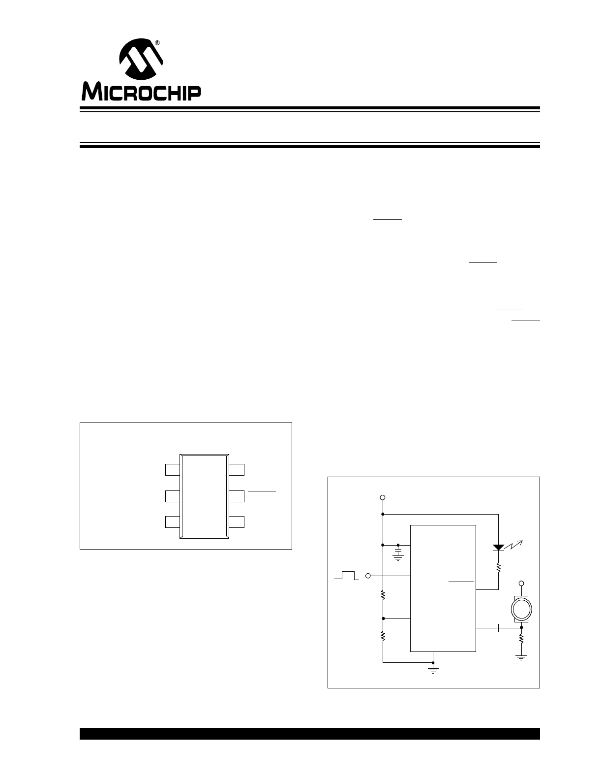
Package Type
General Description
The TC670 is an integrated fan speed sensor that
predicts and/or detects fan failure, preventing thermal
damage to systems with cooling fans. When the fan
speed falls below a user-specified level, the TC670
asserts an ALERT signal. With this design, a critical
minimum fan speed is determined by the user. The fan
alert level is then set with a resistor divider on the
THRESHOLD pin (Pin 1) of the TC670. When the
minimum fan speed is reached, the ALERT pin (Pin 5)
changes from a digital high to low. This failure detection
works with all linear-controlled 2-wire fans. The TC670
eliminates the need for 3-wire fan solutions.
A CLEAR option can be used to reset the ALERT sig-
nal, allowing the flexibility of connecting the ALERT
output of the TC670 with other ALERT/FAULT inter-
rupts in the system. This feature can be implemented
so that false fan fault conditions do not initiate system
shutdown.
The TC670 is specified to operate over the full
industrial temperature range of -40°C to +85°C. The
TC670 is offered in a 6-pin SOT-23 pin package and
consumes 90 µA (typ.) during operation. The space-
saving package and low power consumption make this
device an ideal choice for systems requiring fan speed
monitoring.
Typical Application Circuit
2
5
SOT-23A-6
THRESHOLD
GND
CLEAR
SENSE
ALERT
V
DD
1
3
6
4
TC
670
From
5
6
C
SENSE
R
4
R
SENSE
+12V
ALERT
LED
DC
FAN
DC
FAN
SENSE
ALERT
2
4
3
1
+5V
R
3
R
2
0.1 µF
V
DD
CLEAR
THRESHOLD
GND
Microcontroller
Tiny Predictive Fan Failure Detector
TC670
DS21688D-page 2
2001-2012 Microchip Technology Inc.
1.0
ELECTRICAL
CHARACTERISTICS
Absolute Maximum Ratings†
V
DD
...................................................................................6.0V
All Inputs and Outputs. ............ (GND
0.3V) to (V
DD
+ 0.3V)
Output Short-Circuit Current .................................continuous
Current at Input Pin ................................................... +/-2 mA
Current at Output Pin .............................................. +/-25 mA
Junction Temperature, T
J
............................................. 150°C
ESD protection on all pins
4 kV
Operating Temperature Range........................-40°C to +85°C
Storage Temperature Range .........................-55°C to +150°C
† Notice: Stresses above those listed under "Maximum
Ratings" may cause permanent damage to the device. This is
a stress rating only and functional operation of the device at
those or any other conditions above those indicated in the
operation listings of this specification is not implied. Exposure
to maximum rating conditions for extended periods may affect
device reliability.
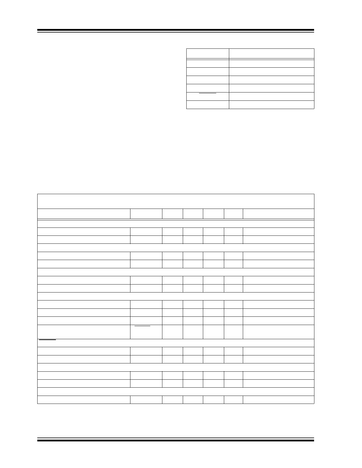
TABLE 1-1:
PIN FUNCTION TABLE
DC CHARACTERISTICS
Symbol
Description
THRESHOLD
Analog Input
GND
Ground Terminal
CLEAR
Digital Input
V
DD
Bias Supply Input
ALERT
Digital (Open-Drain) Output
SENSE
Analog Input
Electrical Specifications: Unless otherwise specified, all limits are specified at +25°C, V
DD
= 3.0V to 5.5V,
CLEAR = Low. Boldface type specifications apply for temperature range of -40°C to +85°C.
Parameters
Sym
Min
Typ
Max
Units
Conditions
Power Supply
Supply Voltage
V
DD
3.0
—
5.5
V
Supply Current
I
DD
—
90
150
µA
CLEAR Input
Logic Input High Level
V
IH
0.8V
DD
—
—
V
Logic Input Low Level
V
IL
—
—
0.2V
DD
V
SENSE Input
Input Level Threshold Voltage
V
TH(SENSE)
—
124
—
mV
Input Resistance
R
SENSE
—
50
—
k
THRESHOLD Input
Input Voltage Minimum
—
0.0
—
V
Input Voltage Maximum
—
2.4
—
V
Input Resistance
—
100
—
M
Programmed Fan Speed Alert Accuracy
(Note 1)
ALERT
ACC
-10
—
+10
%
V
DD
= 3.0V
ALERT Output
Output Low Voltage
V
LOW
—
—
0.3
V
I
SINK
= 2.5 mA
Output Delay Time
t
DELAY
—
176
—
ms
Temperature Ranges
Specified Temperature Range
T
A
-40
—
+85
°C
Operating Temperature Range
T
A
-40
—
+125
°C
Thermal Package Resistances
Thermal Resistance, 6L-SOT-23
JA
—
230
—
°C/W
Note 1: The TC670 will operate properly over the entire power supply range of 3.0V to 5.5V. As V
DD
varies from
3.0V, accuracy will degrade based on the percentage of V
DD
, as shown in Section 2.0, “Typical
Performance Curves”.
2001-2012 Microchip Technology Inc.
DS21688D-page 3
TC670
2.0
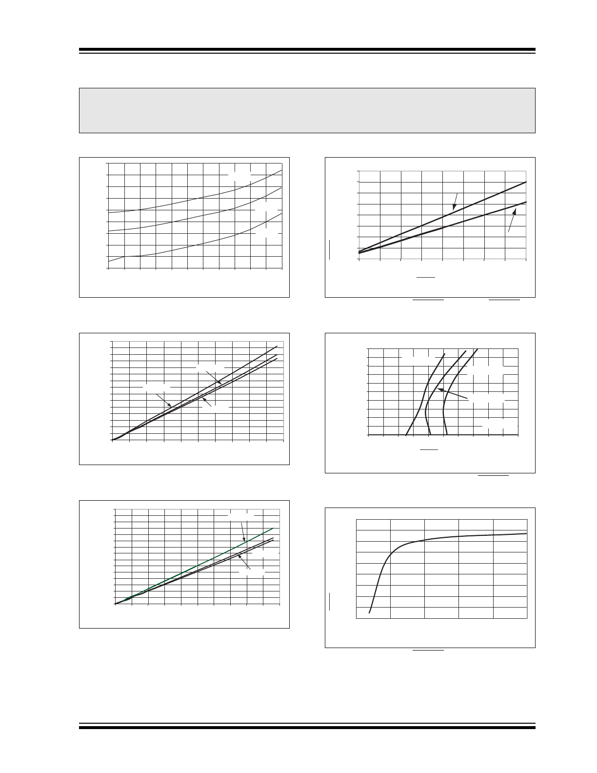
TYPICAL PERFORMANCE CURVES
Note: Unless otherwise indicated, all limits are specified at +25°C, V
DD
= 3.0V to 5.5V, CLEAR = Low.
FIGURE 2-1:
Supply Current vs. Supply
Voltage.
FIGURE 2-2:
Fan Speed vs. Threshold
Voltage.
FIGURE 2-3:
Fan Speed vs. Threshold
Voltage.
FIGURE 2-4:
ALERT V
LOW
vs. ALERT
I
SINK
.
FIGURE 2-5:
Fan Speed vs. ALERT
ACC
.
FIGURE 2-6:
ALERT Output Delay vs.
Power Supply Voltage.
Note:
The graphs and tables provided following this note are a statistical summary based on a limited number of
samples and are provided for informational purposes only. The performance characteristics listed herein
are not tested or guaranteed. In some graphs or tables, the data presented may be outside the specified
operating range (e.g., outside specified power supply range) and therefore outside the warranted range.
+90°C
+25°C
-45°C
115
70
75
80
85
90
95
100
105
110
Supply Current (
μ
A)
Supply Voltage (V)
2.7
3.0
3.3
3.6
3.9
4.2
4.5
4.8
5.1
5.4
5.7
6.0
0
1000
2000
3000
4000
5000
6000
7000
8000
9000
10000
11000
12000
13000
14000
15000
0.00
0.25
0.50
0.75
1.00
1.25
1.50
1.75
2.00
2.25
2.50
THRESHOLD Voltage (V)
Fan Speed (
R
P
M
)
V
DD
= 3.3V
V
DD
= 3.0V
V
DD
= 2.7V
0
1000
2000
3000
4000
5000
6000
7000
8000
9000
10000
11000
12000
13000
14000
15000
0.00
0.25
0.50
0.75
1.00
1.25
1.50
1.75
2.00
2.25
2.50
THRESHOLD Voltage (V)
Fan Speed (
R
P
M
)
V
DD
= 3.6V
V
DD
= 5.5V
V
DD
= 5.0V
0
20
40
60
80
100
120
140
160
0.5
1
1.5
2
2.5
3
3.5
4
4.5
ALERT V
OUT
LOW (mV)
ALERT I
SINK
(mA)
V
DD
= 3.0V
V
DD
= 5.5V
3000
4000
5000
6000
7000
8000
9000
10000
11000
12000
13000
-10.0 -8.0 -6.0 -4.0 -2.0 0.0
2.0
4.0
6.0
8.0 10.0
FA
N
SPEED
(
R
PM
)
ALERT
ACC
(%)
V
DD
= 3.0V
T
A
= -40˚C
T
A
= +25˚C
T
A
= +90˚C
168
169
170
171
172
173
174
175
176
177
2.5
3.0
3.5
4.0
4.5
5.0
Power Supply Voltage (V
DD
)
AL
E
R
T
Output Delay Time (
m
s)
TC670
DS21688D-page 4
2001-2012 Microchip Technology Inc.
Note: Unless otherwise indicated, all limits are specified at +25°C, V
DD
= 3.0V to 5.5V, CLEAR = Low.
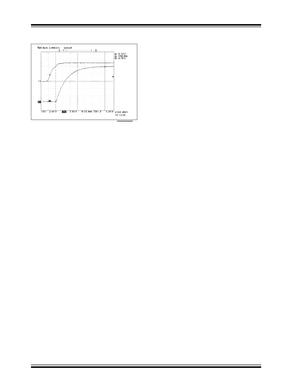
FIGURE 2-7:
CLEAR pin high to ALERT
pin high Timing Diagram.
2001-2012 Microchip Technology Inc.
DS21688D-page 5
TC670
3.0
PIN DESCRIPTIONS
The descriptions of the pins are listed in Table 3-1.
TABLE 3-1:
PIN FUNCTION TABLE
3.1
Analog Input (THRESHOLD)
The voltage set at the THRESHOLD input represents
the fan speed at which the TC670 will signal a fan
speed warning by pulling the ALERT output low. The
threshold voltage to fan speed correlation can be seen
in Figures 2-2 and 2-3.
3.2
Ground (GND)
The GND pin (Pin 2) of the TC670 should be connected
directly to the analog ground plane of the circuit board.
Care should be taken to keep this pin away from
switching signals, such as the fan excitation signals in
order to avoid false signals on the SENSE pin.
3.3
Digital Input (CLEAR)
The CLEAR input is used to reset or blank the ALERT
output. When the CLEAR input is driven high, the
ALERT output will be high-impedance (the ALERT
output requires a pull-up resistor).
3.4
Bias Supply Input (V
DD
)
Bias Supply Input, 3.0V to 5.5V. The bias supply input
should be bypassed to ground with a 0.1 µF ceramic
capacitor.
3.5
Digital (Open-Drain) Output
(ALERT)
The ALERT output is an open-drain output that
requires an external pull-up resistor. The ALERT output
is pulled low when the sensed fan speed (detected by
the pulses occurring at the SENSE input) falls below
the speed that is represented by the voltage at the
THRESHOLD pin. The ALERT output is latched in this
state until power is cycled or the CLEAR input is
toggled.
3.6
Analog Input (SENSE)
Voltage pulses, which are generated by the fan current
flowing through a sense resistor, are detected at the
SENSE pin and used to calculate the fan speed.
Pin
No.
Symbol
Description
1
THRESHOLD
Analog Input
2
GND
Ground Terminal
3
CLEAR
Digital Input
4
V
DD
Bias Supply Input
5
ALERT
Digital (Open-Drain) Output
6
SENSE
Analog Input
TC670
DS21688D-page 6
2001-2012 Microchip Technology Inc.
4.0
DETAILED DESCRIPTION
The TC670 is an integrated fan speed sensor that
predicts/detects fan failure, consequently preventing
thermal damage to systems with cooling fans. When
the fan speed falls below a user-programmed threshold
level, the TC670 asserts an ALERT signal. This
threshold is set with an external resistor divider
network.
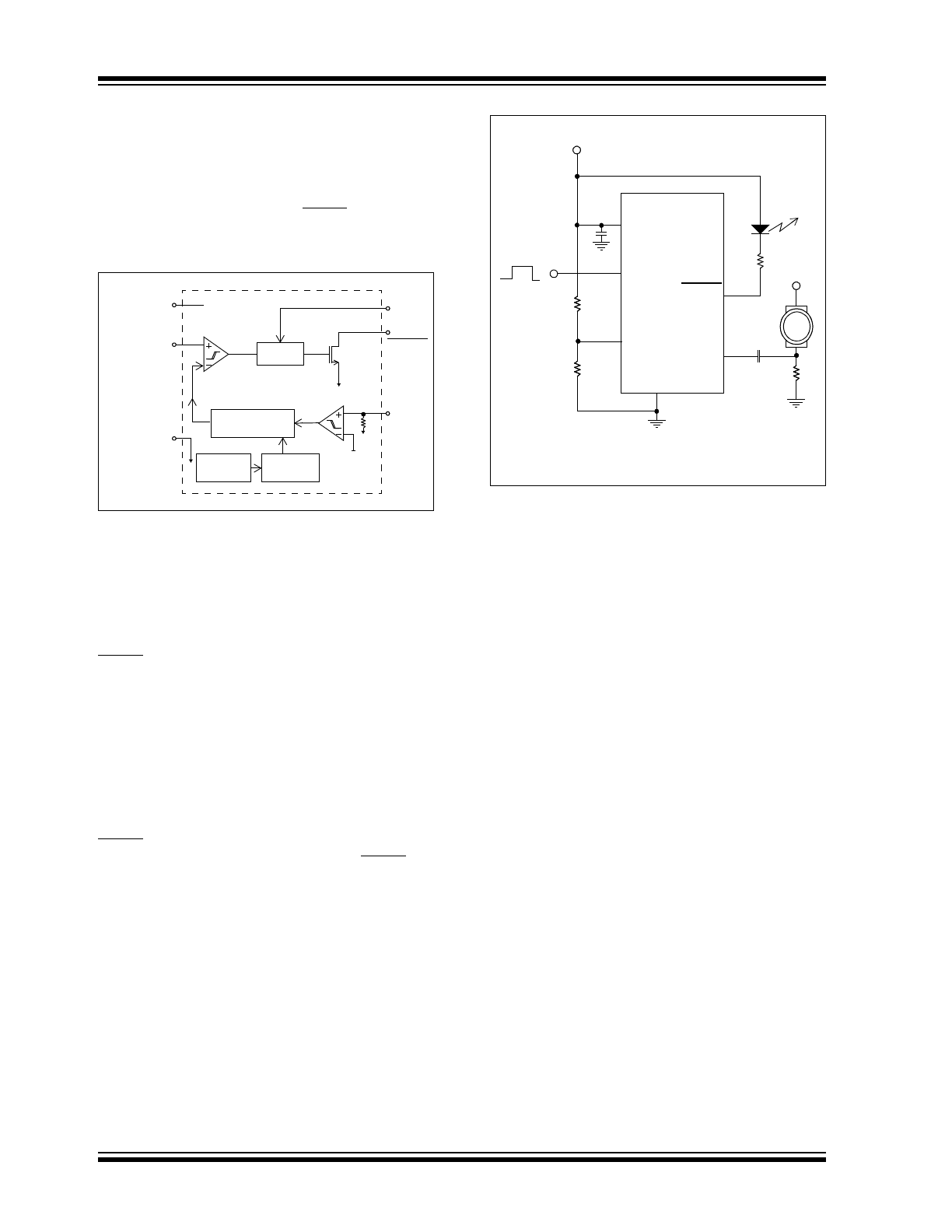
FIGURE 4-1:
TC670 Block Diagram.
As shown in Figure 4-1, the TC670 senses the fan
pulses and internally converts those pulses from a
frequency into an analog voltage. This voltage is then
compared with the DC voltage at the THRESHOLD pin.
If the converted frequency-to-voltage value from the
fan's pulses falls below the threshold voltage, the
ALERT output is pulled low.
In a 3.0V system, the external fan alert level on the
THRESHOLD pin can be designed from 0.0V (stalled
fan) to 2.4V (for 13,000 RPM) to cover most of the com-
mon fan speeds. This failure detection system works
with linear-controlled 2-wire fans and eliminates the
need for 3-wire fans. The TC670 can also work with
3-wire fans either by using the SENSE circuit or by
directly sensing the RPM output from the 3rd wire.
A CLEAR pin is provided to allow the user to reset the
ALERT pin status back to a high state. This clear option
also allows the flexibility of connecting the ALERT out-
put of the TC670 with other alert/fault interrupts in the
system without having a risk of a system shutdown due
to false fan fault condition.
FIGURE 4-2:
Typical Application Circuit.
4.1
SENSE Input
As shown in Figure 4-2, the SENSE input (Pin 6) is
connected to the sense resistor (R
SENSE
) through a
capacitor (C
SENSE
). The low value current sensing
resistor (R
SENSE
) is connected between the ground
return leg of the fan and the fan bias ground. During
normal fan operation, commutation occurs as each
pole of the fan is energized. This causes the fan current
to be an AC waveform with fast falling edges.
These short, rapid changes in fan current cause a
corresponding dV/dt voltage across the sense resistor,
as well as a corresponding dI/dt current through the
sense capacitor. The current through C
SENSE
is termi-
nated with the internal 50 k
input resistance at the
SENSE pin of the TC670. When positive-going fan
pulses at the SENSE input are greater than 124 mV
(typ.), the TC670 latches-in those voltage spikes. This
124 mV (typ.) SENSE input built-in threshold reduces
false triggering errors caused by extraneous noise
pulses associated with a running fan. The presence
and frequency of these pulses is a direct indication of
fan operation and fan speed.
THRESHOLD
124 mV
50 k
SENSE
ALERT
CLEAR
Logic
Frequency-to-
Voltage
GND
V
DD
Bandgap
Oscillator
Note: This typical application circuit uses a LED to
indicate that a fan failure has occurred.
5
6
C
SENSE
R
4
R
SENSE
+12V
ALERT
LED
DC
FAN
DC
FAN
SENSE
ALERT
2
4
3
1
+5V
R
3
R
2
0.1 µF
V
DD
CLEAR
THRESHOLD
GND
2001-2012 Microchip Technology Inc.
DS21688D-page 7
TC670
The design of the proper input SENSE circuitry is a
matter of scaling R
SENSE
to provide the necessary
amount of gain and proper selection of the sensing
capacitor. The following table (Table 4-1) lists some
recommended values for R
SENSE
according to the
nominal operating current of the fan. Please note that
the current draw specified by the fan manufacturer may
be a worst-case rating and not the fan’s nominal oper-
ating current. If the fan current falls between two of the
values listed, it is recommended that the higher value
resistor is used.
TABLE 4-1:
RECOMMENDED VALUES
FOR R
SENSE
PER FIGURE 4-2
A 0.1 µF ceramic capacitor is recommended for
C
SENSE
. Smaller capacitor values will require larger
sense resistors, whereas larger capacitors are more
expensive and occupy more board space.
4.2
THRESHOLD Input
The voltage at the THRESHOLD input sets the
equivalent minimum allowable fan speed for the appli-
cation. As shown in Section 2.0, “Typical Performance
Curves”, the relationship between the threshold voltage
and minimum fan speed is also power supply and tem-
perature dependant.
All the values for the threshold voltage that are shown in
these graphs represent typical numbers and might not
be optimized for all fans in all applications. To ensure
accurate fan speed monitoring of a specific fan in a spe-
cific application, the user must perform a one-time cor-
relation check with the prototype.
There are two techniques that can be used to calibrate
the system. One approach is to find the fan’s full-scale
capability and mathematically estimate the minimum
acceptable speed of the fan. A second technique is to
identify the fan’s minimum speed and calibrate the
threshold voltage accordingly.
4.2.1
THRESHOLD CALIBRATION USING
FAN’S FULL SCALE SPEED
The fan should first be run at full speed. At full speed,
the threshold voltage level should be adjusted until the
ALERT output is asserted. With this full-scale value of
the threshold voltage, the value can be scaled down to
the fan fault speed as a percentage of the full speed.
For example, if the fan full speed threshold voltage is
1.5V, then the fan fault threshold voltage at 30% of full
speed would be 30% x 1.5V = 0.45V.
4.2.2
THRESHOLD CALIBRATION USING
FAN’S MINIMUM ALLOWABLE
SPEED ESTIMATE
For a more exact fan fault trip point, the user can run
the fan at its minimum allowed speed. At this speed, the
threshold voltage can be adjusted until the ALERT out-
put is asserted.
4.3
CLEAR Input
The CLEAR input allows the user to reset the ALERT
pin to a high status. This is an active-high input.
Consequently, as long as CLEAR is high, ALERT will
always be high as well. To allow ALERT to operate cor-
rectly, CLEAR must be held low.
This feature can be
implemented so that false fan fault conditions do not
initiate system shutdown.
4.4
ALERT Output
The ALERT output is an open-drain output capable of
sinking 2.5 mA (typ). The ALERT output is asserted
whenever the detected fan speed equals or falls below
the equivalent voltage set at the threshold pin. The
ALERT output is only deactivated once the CLEAR pin
is brought to a high state. Although the absolute
maximum sink current of this pin is 25 mA, it is
recommended that the current sinking into the ALERT
output does not exceed 20 mA.
4.5
Power Supply Input (V
DD
)
To assure proper operation of the TC670 in a noisy
environment where the fans are running, the V
DD
pin
(Pin 4) must be decoupled with a 0.1 µF capacitor, as
shown in Figure 4-1. This capacitor should be located
as close to the TC670 V
DD
pin as possible, as well as
being promptly terminated to the ground plane. A
ceramic capacitor is recommended.
4.6
Ground Terminal (GND)
The GND pin (Pin 2) of the TC670 should be connected
directly to the analog ground plane of the circuit board.
Care should be taken to keep this pin away from
switching signals, such as the fan excitation signals in
order to avoid false signals on the SENSE pin.
Nominal Fan Current
(mA)
R
SENSE
(
)
100
4.7
200
2.4
300
1.8
400
1.3
500
1.0
600
0.8
TC670
DS21688D-page 8
2001-2012 Microchip Technology Inc.
5.0
PACKAGE INFORMATION
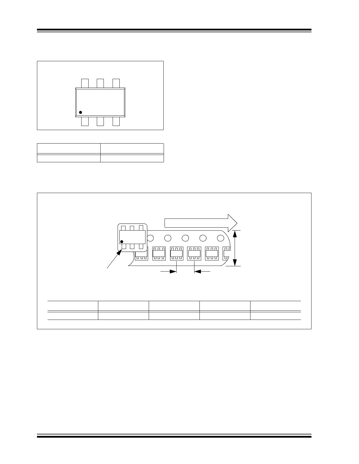
5.1
Package Marking Information
1 & 2 = part number code
3 = year and quarter code
4 = lot ID number
5.2
Taping Form
Part Number
Code
TC670ECH
DA
5
2
4
6
3
1
6-Pin SOT-23A (EIAJ SC-74) Device
Component Taping Orientation for 6-Pin SOT-23A (EIAJ SC-74) Devices
Carrier Tape, Number of Components Per Reel and Reel Size:
Package
Carrier Width (W)
Pitch (P)
Part Per Full Reel
Reel Size
6-Pin SOT-23A
8 mm
4 mm
3000
7 in.
Device
Marking
PIN 1
User Direction of Feed
W
P
2001-2012 Microchip Technology Inc.
DS21688D-page 9
TC670
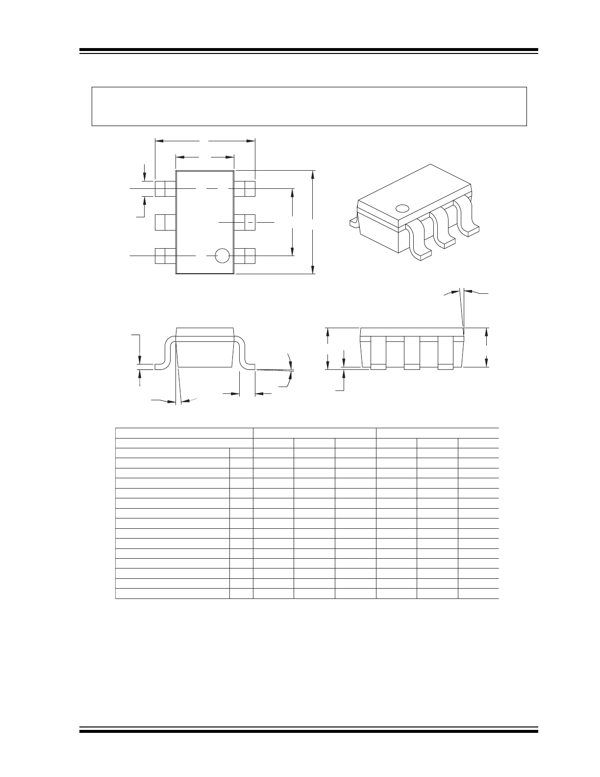
5.3
Package Dimensions (6-Pin SOT-23)
10
5
0
10
5
0
Mold Draft Angle Bottom
10
5
0
10
5
0
Mold Draft Angle Top
0.50
0.43
0.35
.020
.017
.014
B
Lead Width
0.20
0.15
0.09
.008
.006
.004
c
Lead Thickness
10
5
0
10
5
0
Foot Angle
0.55
0.45
0.35
.022
.018
.014
L
Foot Length
3.10
2.95
2.80
.122
.116
.110
D
Overall Length
1.75
1.63
1.50
.069
.064
.059
E1
Molded Package Width
3.00
2.80
2.60
.118
.110
.102
E
Overall Width
0.15
0.08
0.00
.006
.003
.000
A1
Standoff
1.30
1.10
0.90
.051
.043
.035
A2
Molded Package Thickness
1.45
1.18
0.90
.057
.046
.035
A
Overall Height
1.90
.075
p1
Outside lead pitch (basic)
0.95
.038
p
Pitch
6
6
n
Number of Pins
MAX
NOM
MIN
MAX
NOM
MIN
Dimension Limits
MILLIMETERS
INCHES*
Units
1
D
B
n
E
E1
L
c
A2
A
A1
p1
exceed .005" (0.127mm) per side.
Dimensions D and E1 do not include mold flash or protrusions. Mold flash or protrusions shall not
Notes:
JEITA (formerly EIAJ) equivalent: SC-74A
Drawing No. C04-120
*Controlling Parameter
Note:
For the most current package drawings, please see the Microchip Packaging Specification located
at http://www.microchip.com/packaging

TC670
DS21688D-page 10
2001-2012 Microchip Technology Inc.
6.0
REVISION HISTORY
Revision D (December 2012)
Added a note to each package outline drawing.